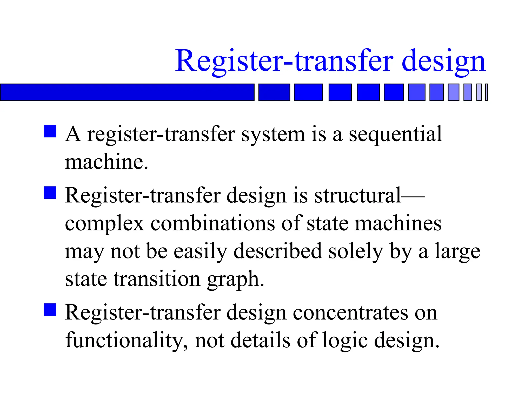
Register-transfer design
Aregister-transfer system is a sequential
machine.
Register-transfer design is structural—
complex combinations of state machines
may not be easily described solely by a large
state transition graph.
Register-transfer design concentrates on
functionality, not details of logic design.
3.
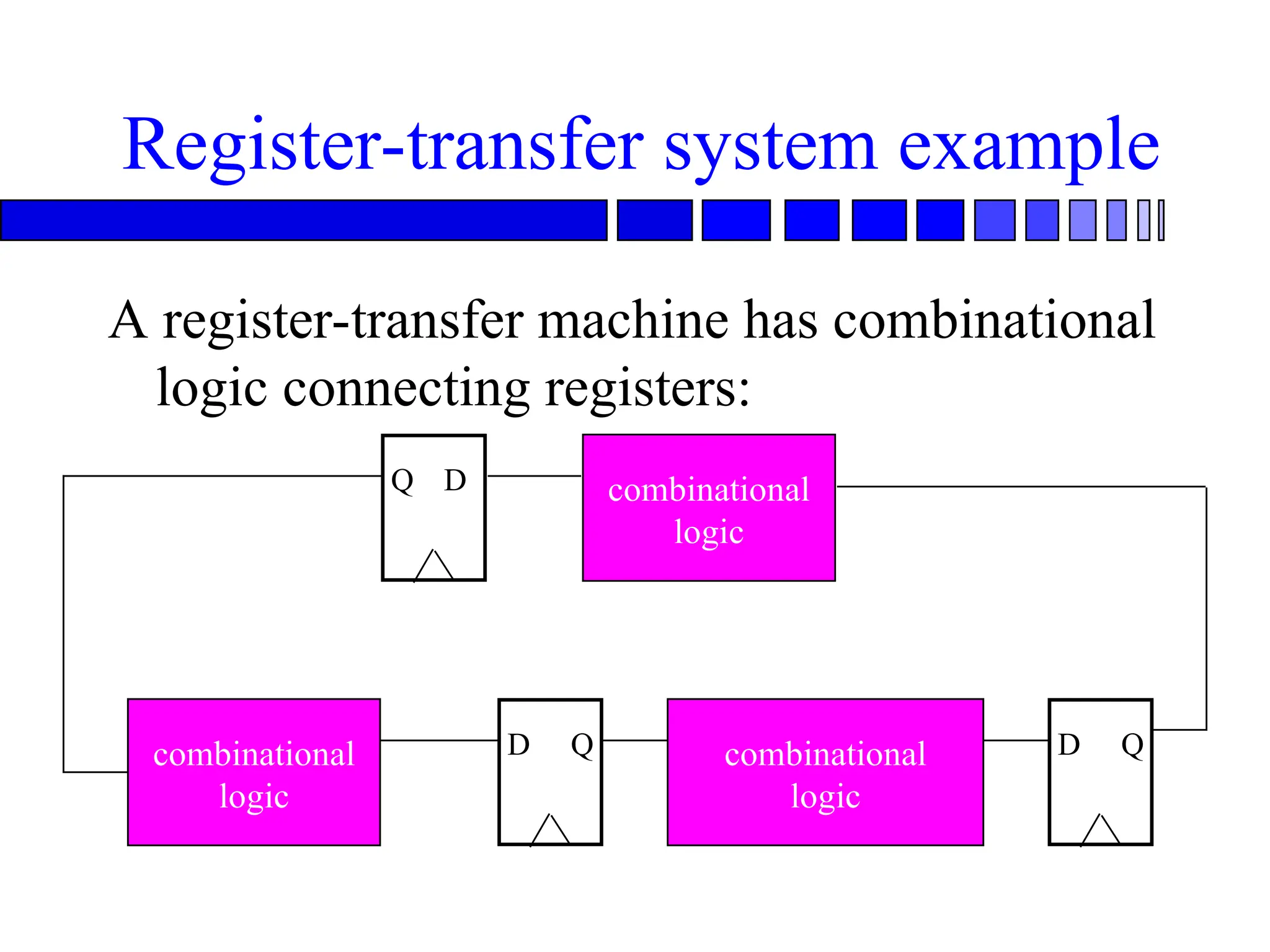
Register-transfer system example
Aregister-transfer machine has combinational
logic connecting registers:
D
Q combinational
logic
D Q
D Q combinational
logic
combinational
logic
4.
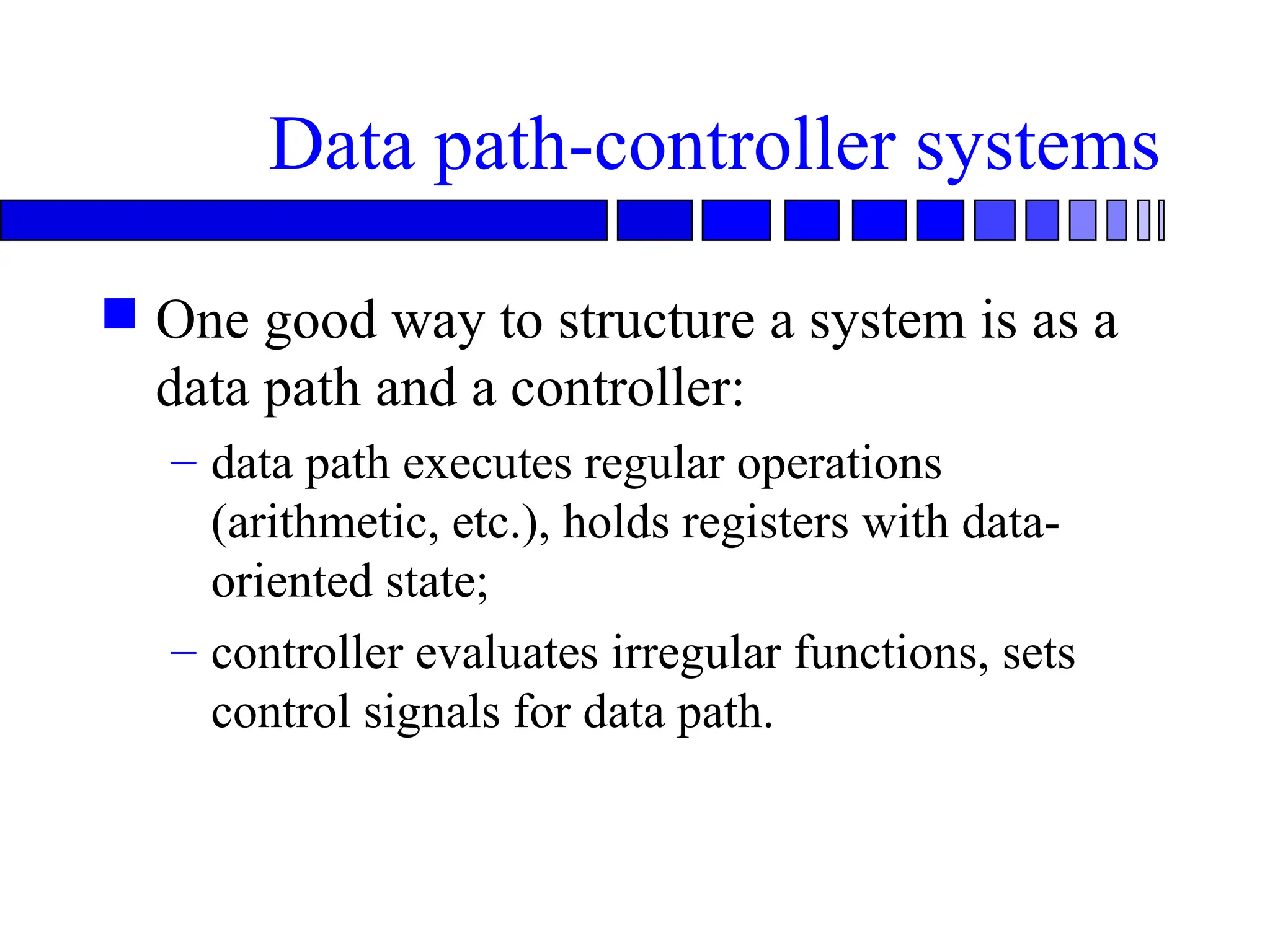
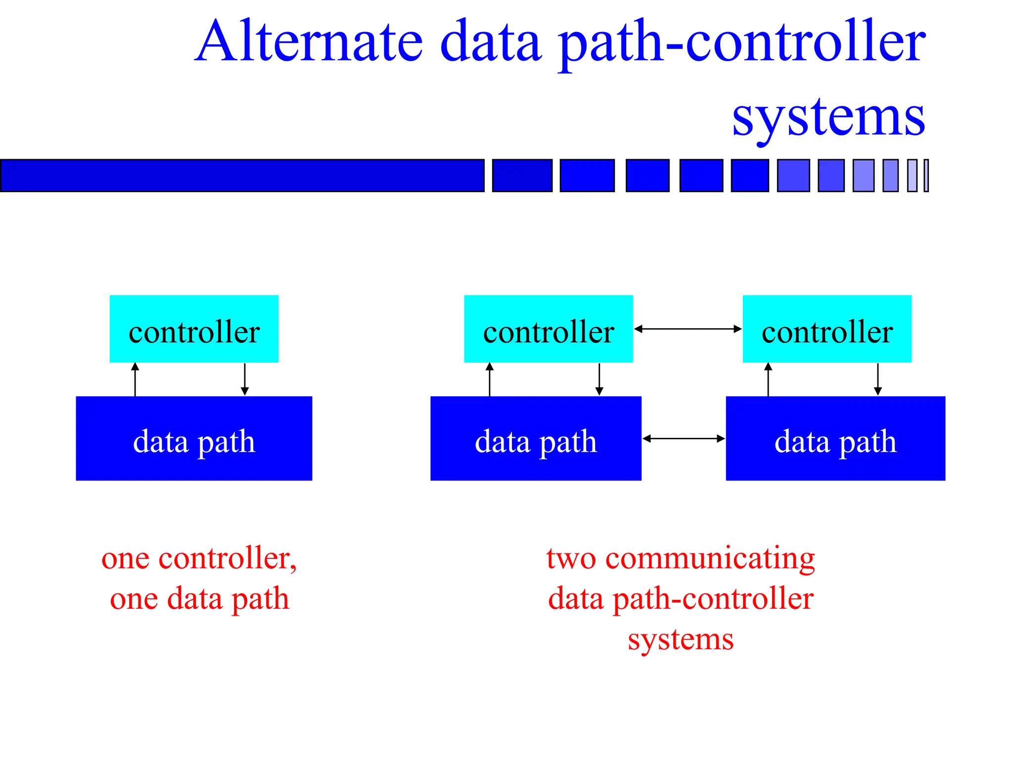
Data path-controller systems
One good way to structure a system is as a
data path and a controller:
– data path executes regular operations
(arithmetic, etc.), holds registers with data-
oriented state;
– controller evaluates irregular functions, sets
control signals for data path.
5.
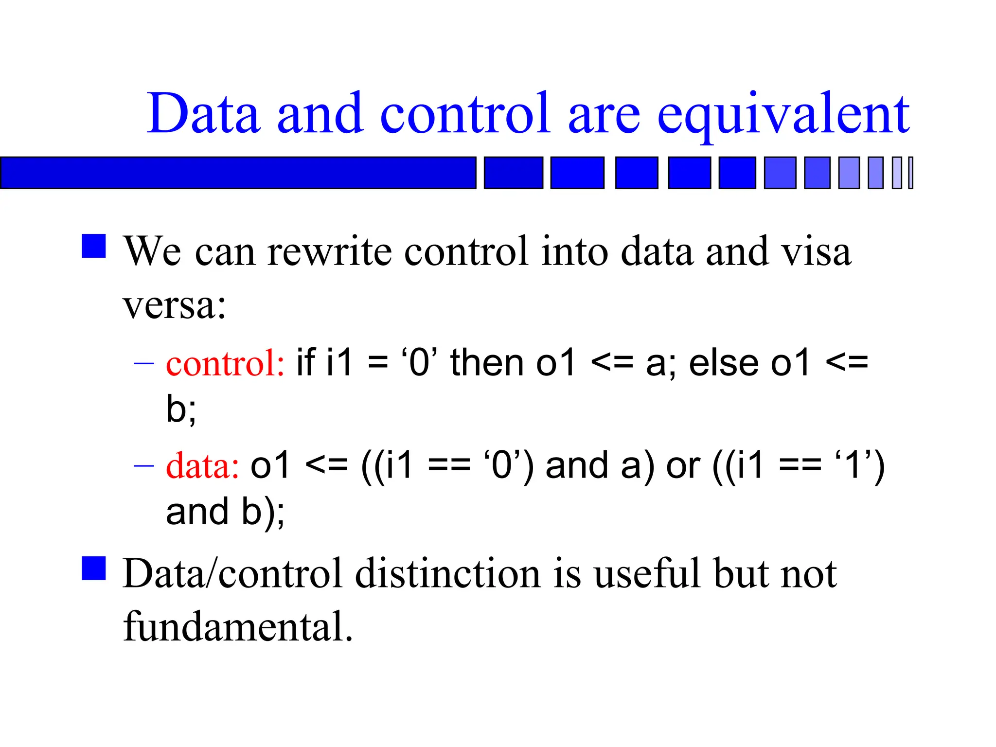
Data and controlare equivalent
We can rewrite control into data and visa
versa:
– control: if i1 = ‘0’ then o1 <= a; else o1 <=
b;
– data: o1 <= ((i1 == ‘0’) and a) or ((i1 == ‘1’)
and b);
Data/control distinction is useful but not
fundamental.
6.
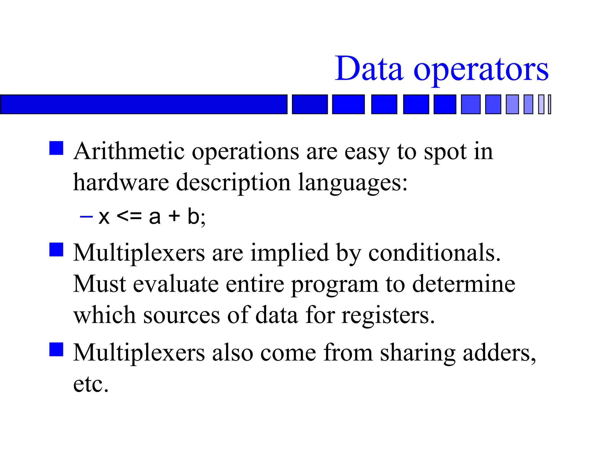
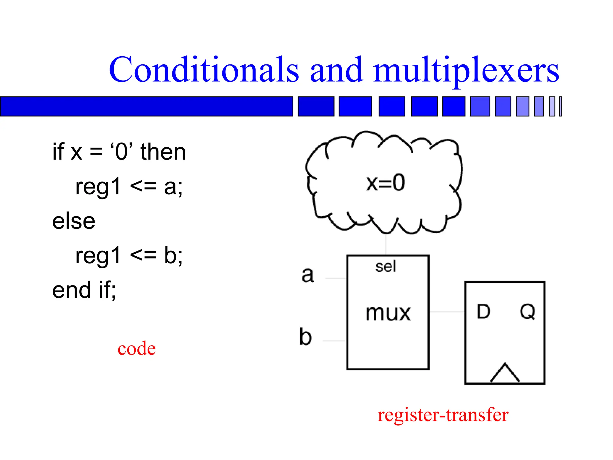
Data operators
Arithmeticoperations are easy to spot in
hardware description languages:
– x <= a + b;
Multiplexers are implied by conditionals.
Must evaluate entire program to determine
which sources of data for registers.
Multiplexers also come from sharing adders,
etc.
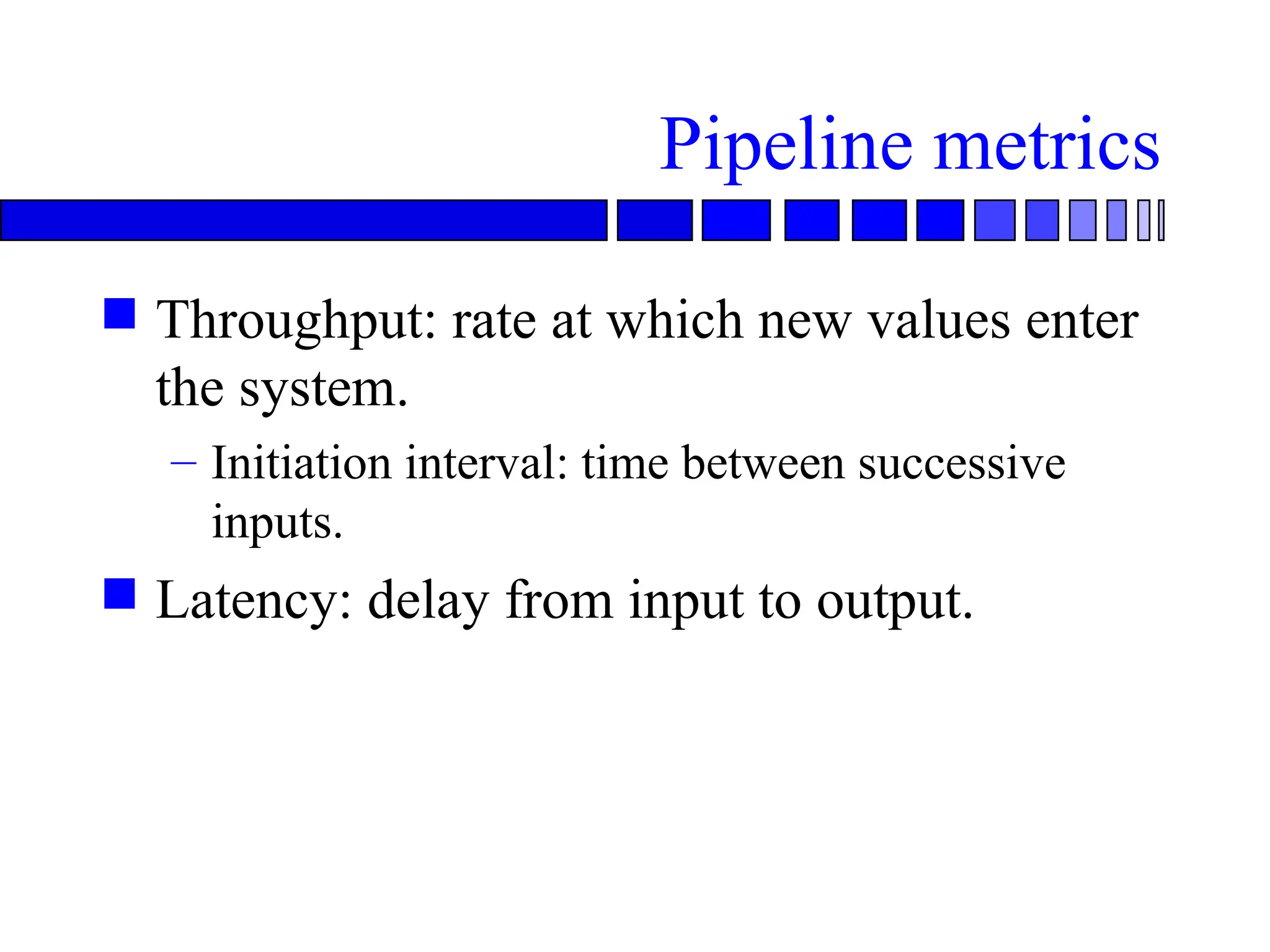
Pipeline metrics
Throughput:rate at which new values enter
the system.
– Initiation interval: time between successive
inputs.
Latency: delay from input to output.
11.
High-level synthesis
Sequentialoperation is not the most abstract
description of behavior.
We can describe behavior without assigning
operations to particular clock cycles.
High-level synthesis (behavioral synthesis)
transforms an unscheduled behavior into a
register-transfer behavior.
12.
Tasks in high-levelsynthesis
Scheduling: determines clock cycle on
which each operation will occur.
Allocation: chooses which function units
will execute which operations.
13.
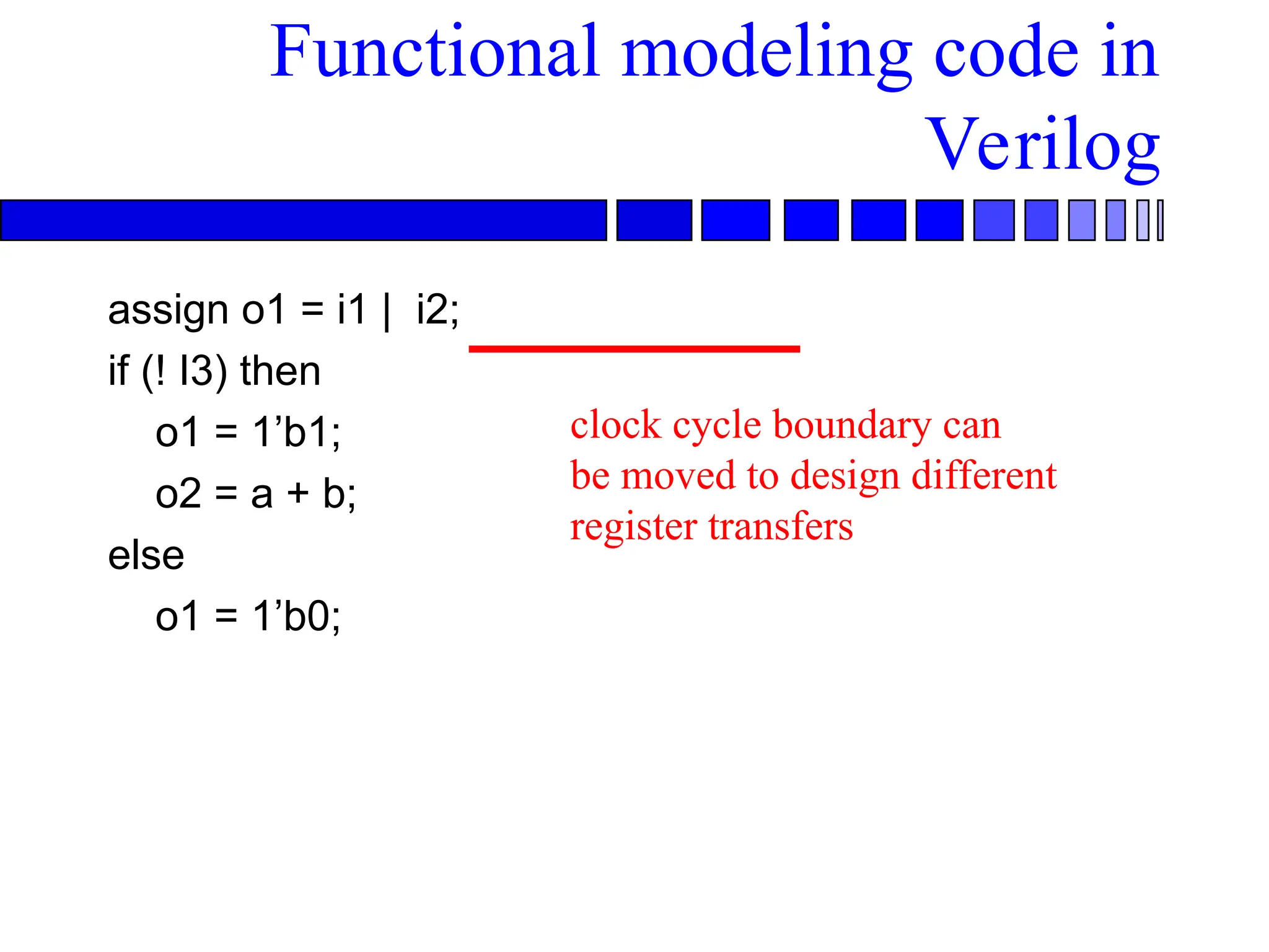
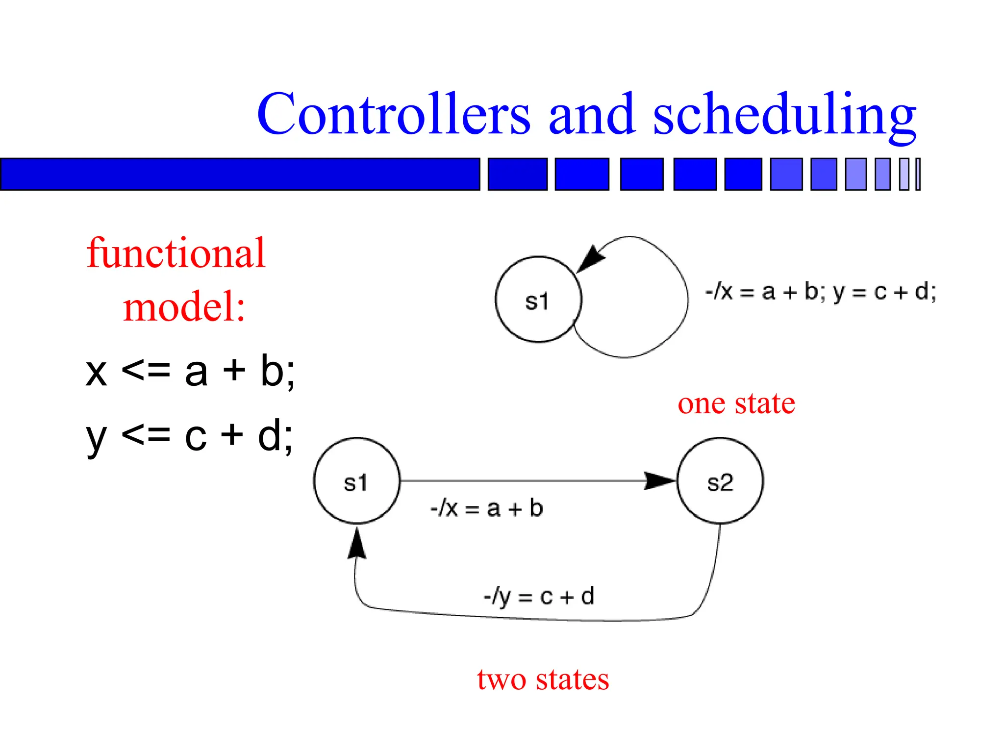
Functional modeling codein
Verilog
assign o1 = i1 | i2;
if (! I3) then
o1 = 1’b1;
o2 = a + b;
else
o1 = 1’b0;
clock cycle boundary can
be moved to design different
register transfers
14.
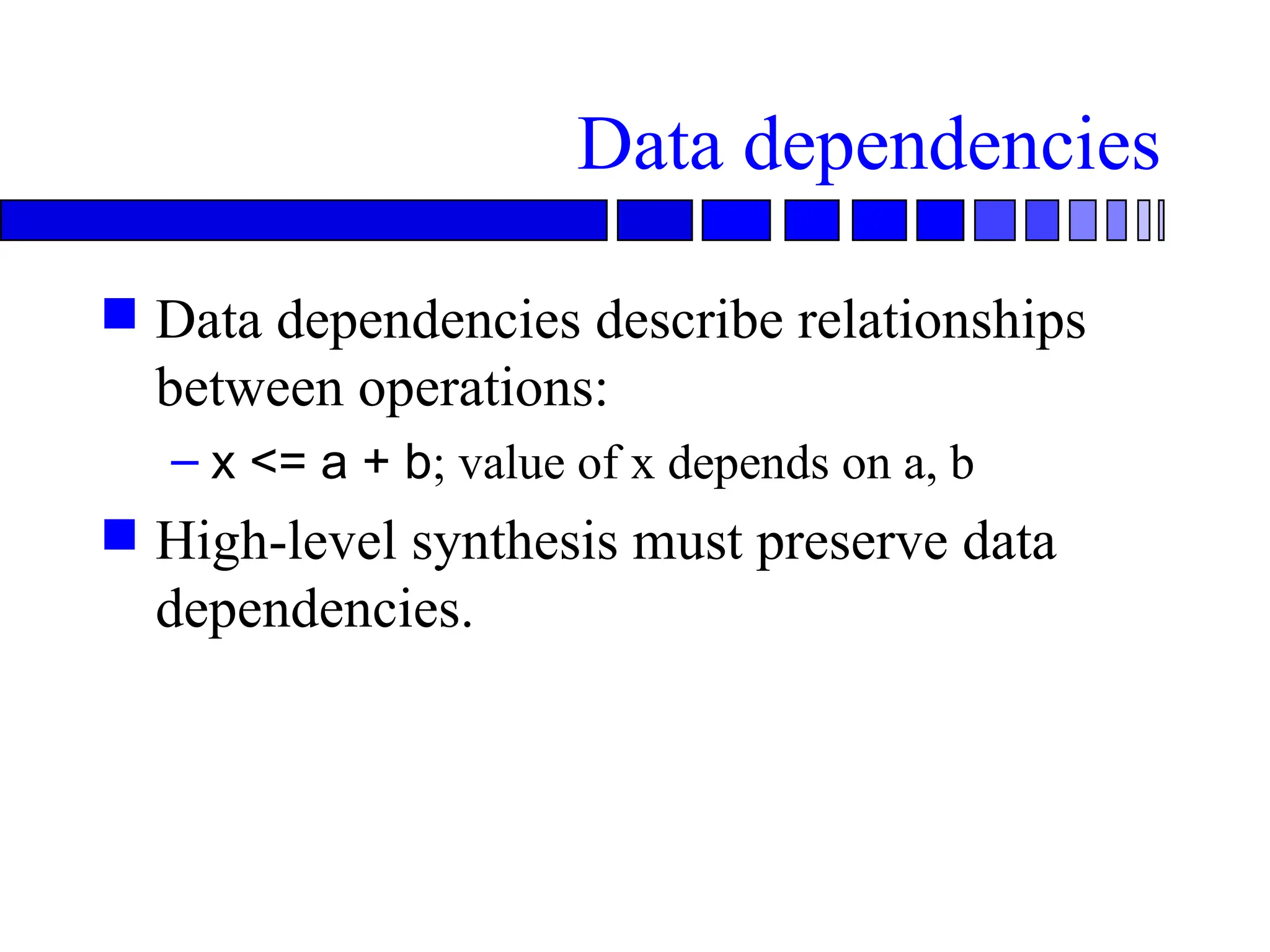
Data dependencies
Datadependencies describe relationships
between operations:
– x <= a + b; value of x depends on a, b
High-level synthesis must preserve data
dependencies.
15.
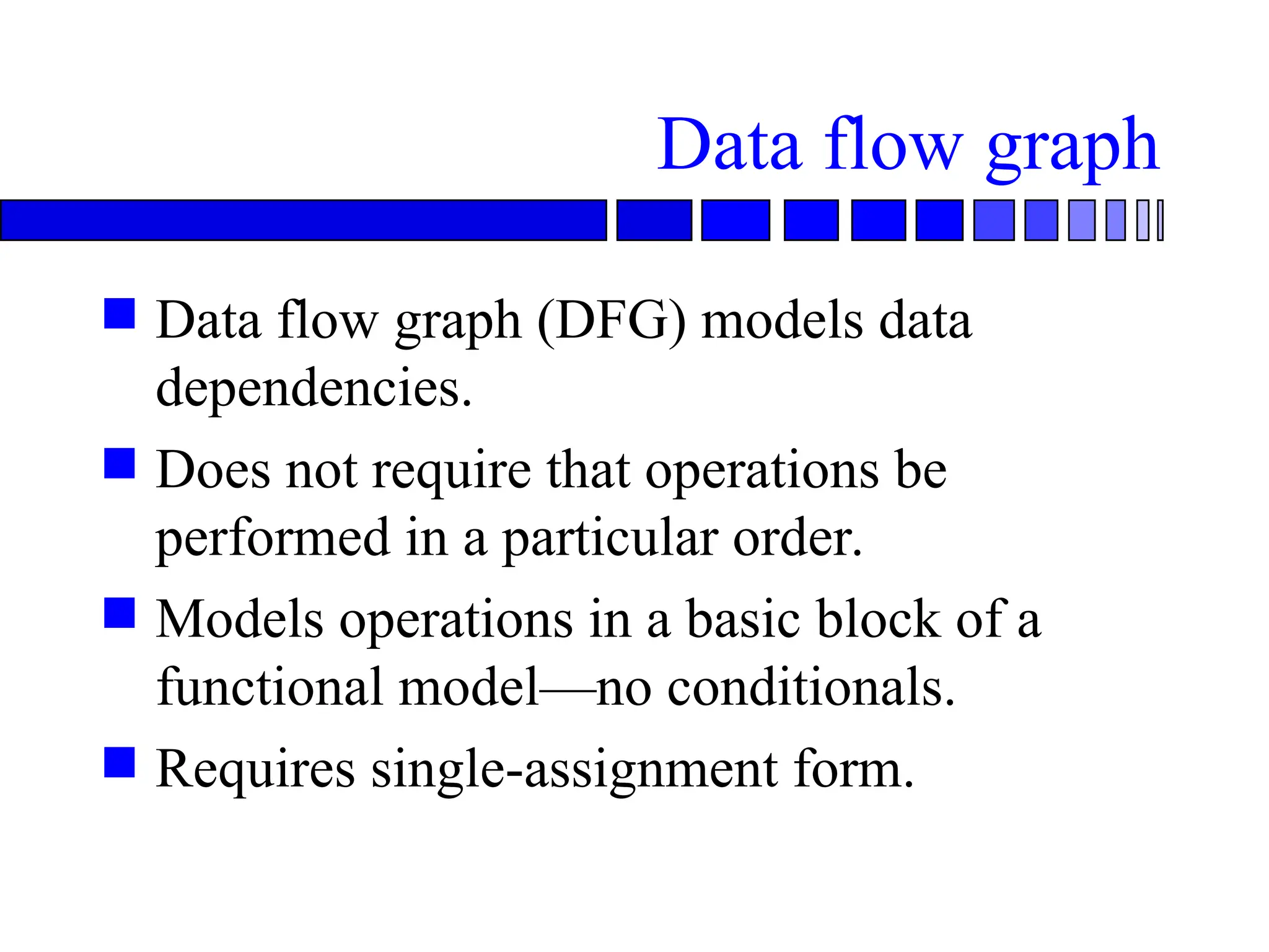
Data flow graph
Data flow graph (DFG) models data
dependencies.
Does not require that operations be
performed in a particular order.
Models operations in a basic block of a
functional model—no conditionals.
Requires single-assignment form.
16.
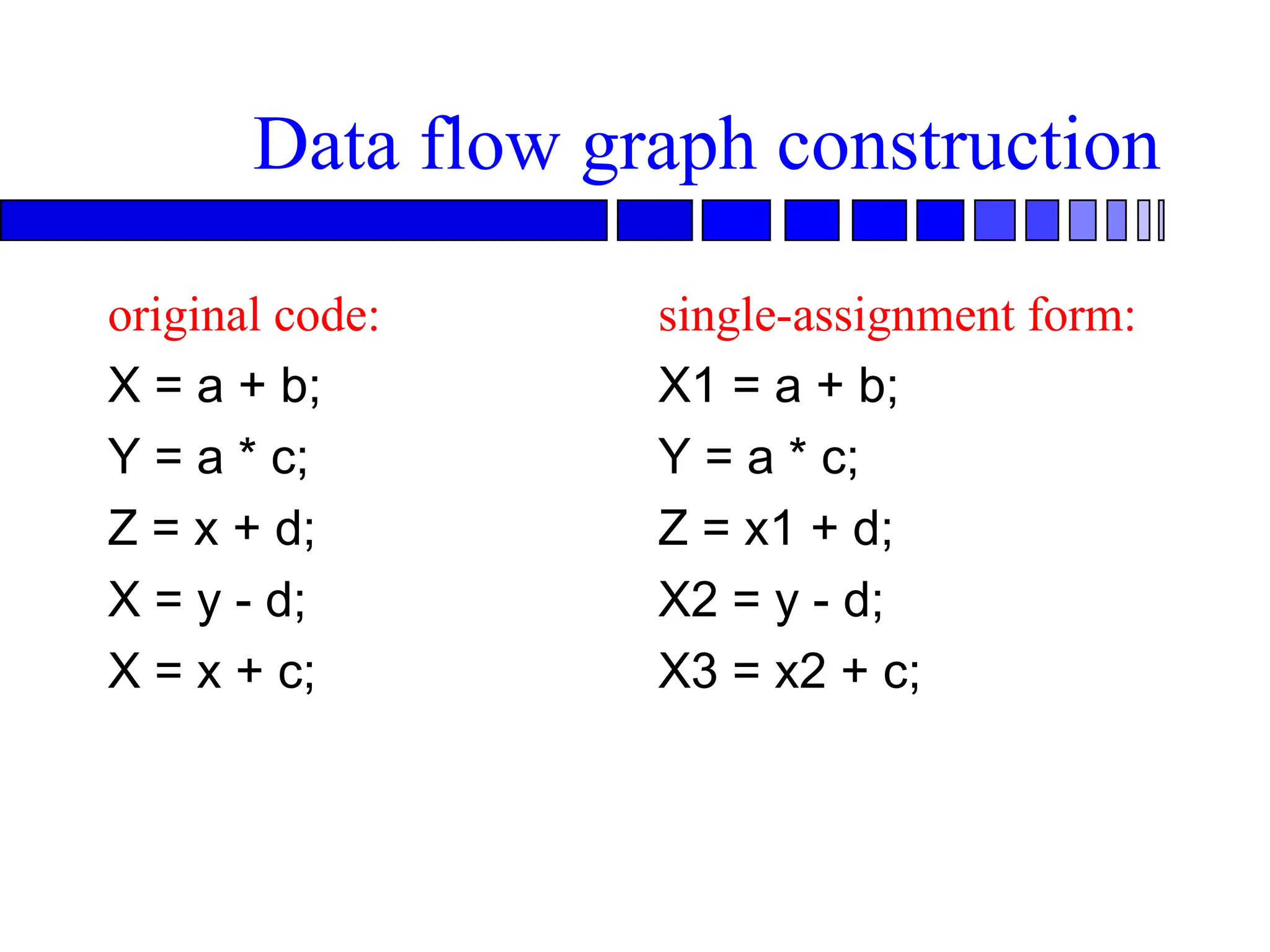
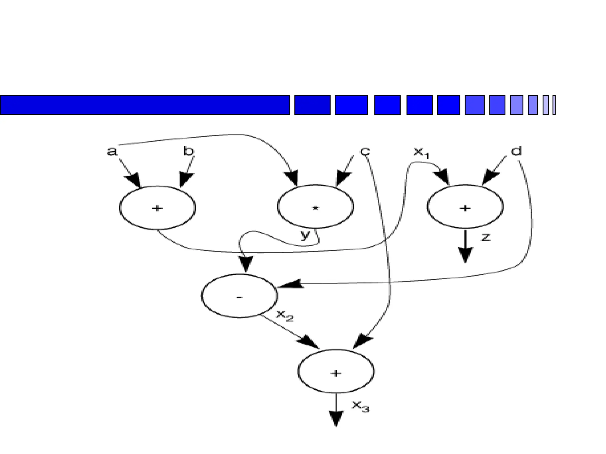
Data flow graphconstruction
original code:
X = a + b;
Y = a * c;
Z = x + d;
X = y - d;
X = x + c;
single-assignment form:
X1 = a + b;
Y = a * c;
Z = x1 + d;
X2 = y - d;
X3 = x2 + c;
17.
Data flow graphconstruction,
cont’d
Data flow forms directed acyclic graph
(DAG): All edges are directed and there is
no cycle of edges that form a path from a
node back to that node.
19.
Goals of schedulingand
allocation
Preserve behavior—at end of execution,
should have received all outputs, be in
proper state (ignoring exact times of
events).
Utilize hardware efficiently.
Obtain acceptable performance.
20.
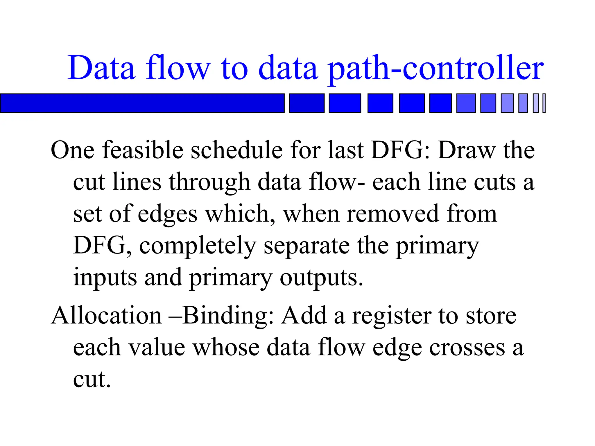
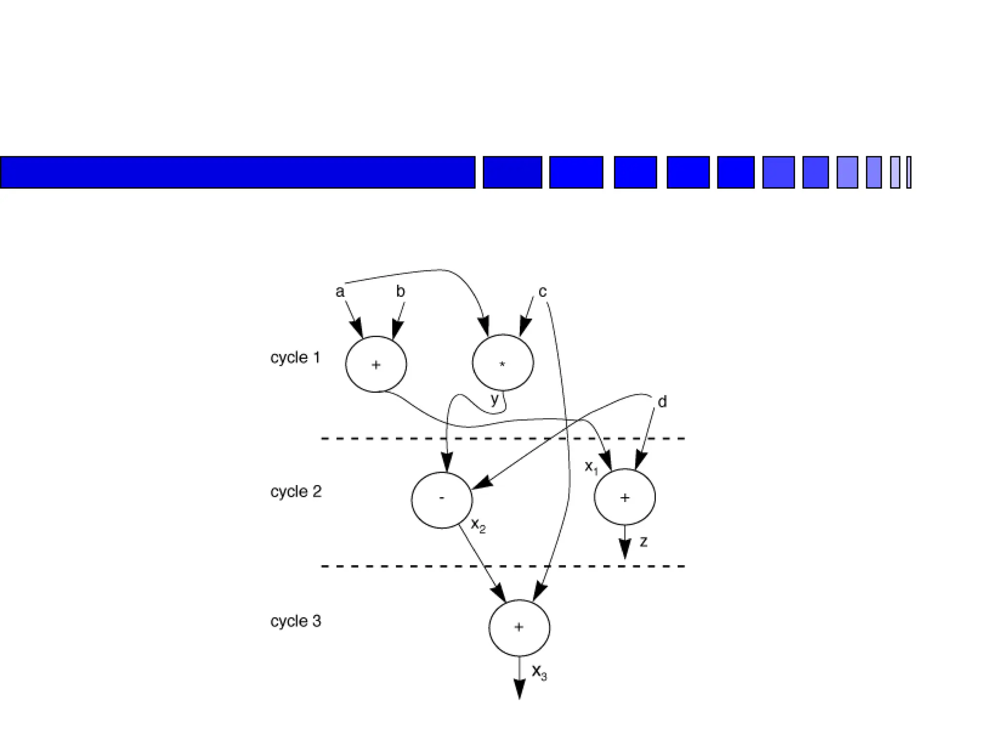
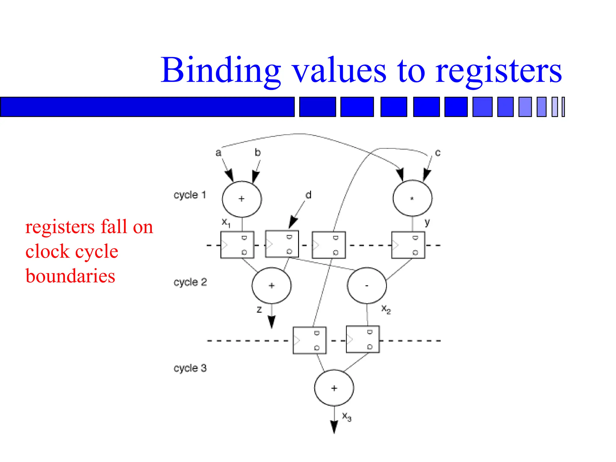
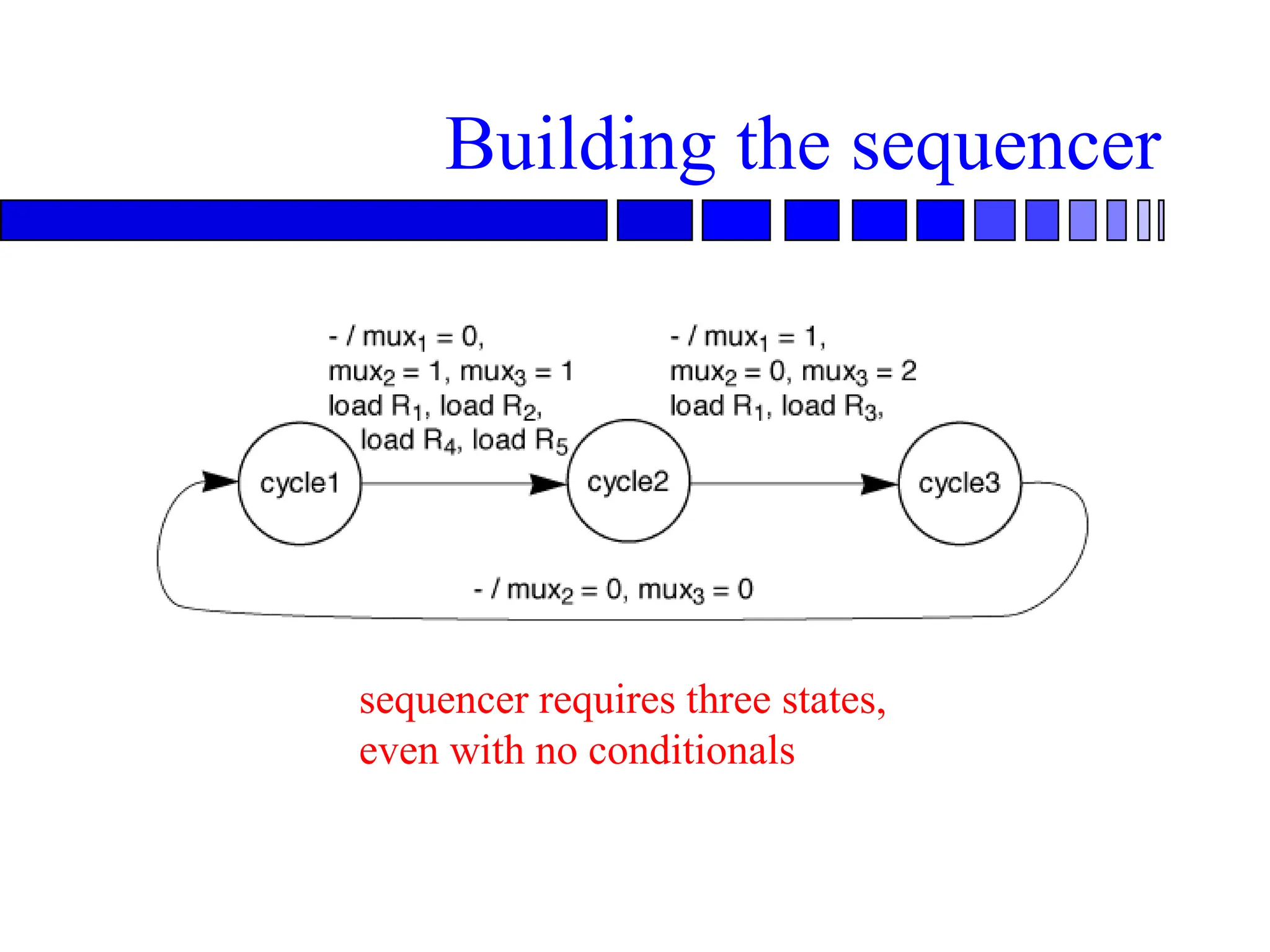
Data flow todata path-controller
One feasible schedule for last DFG: Draw the
cut lines through data flow- each line cuts a
set of edges which, when removed from
DFG, completely separate the primary
inputs and primary outputs.
Allocation –Binding: Add a register to store
each value whose data flow edge crosses a
cut.
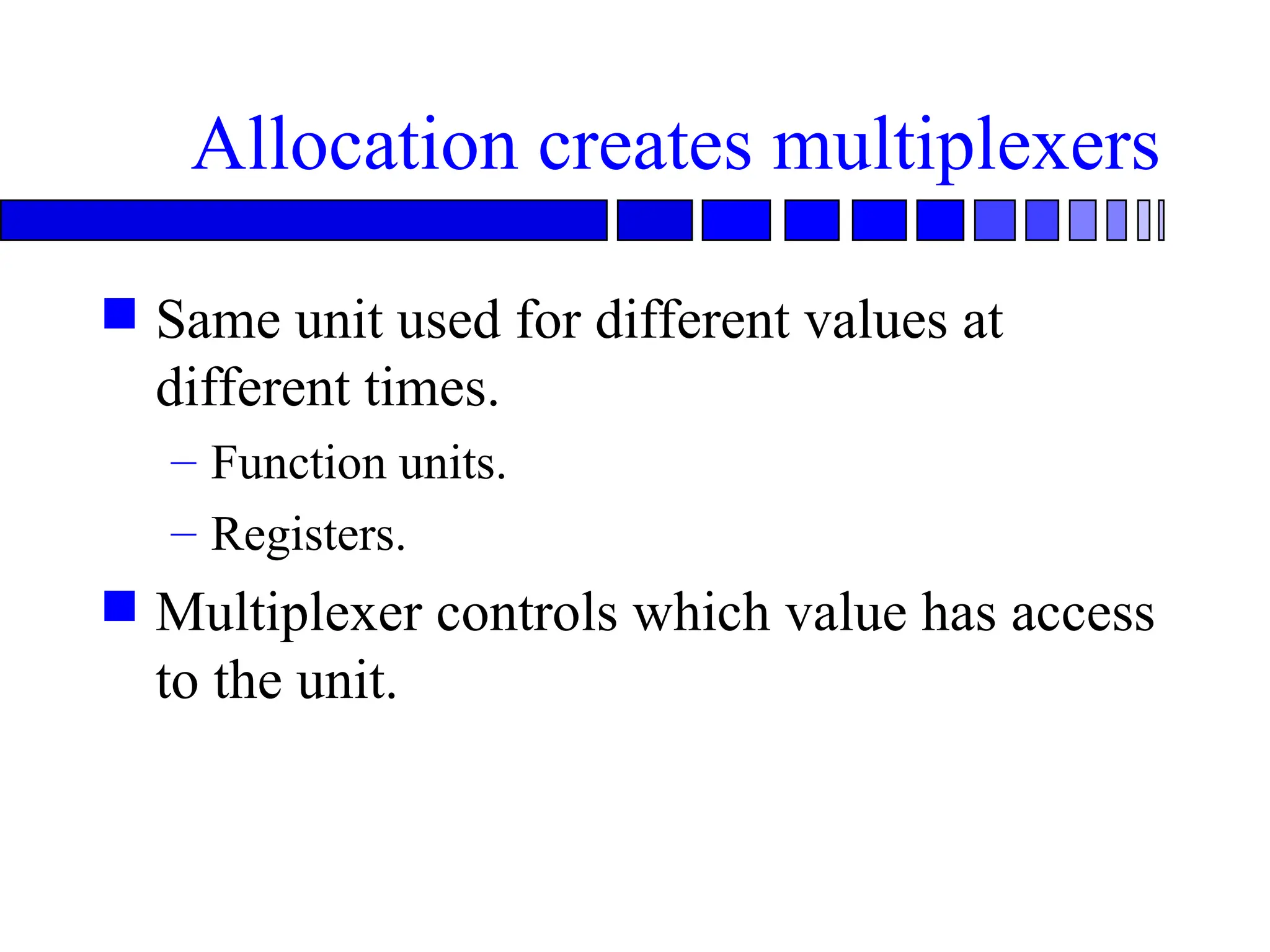
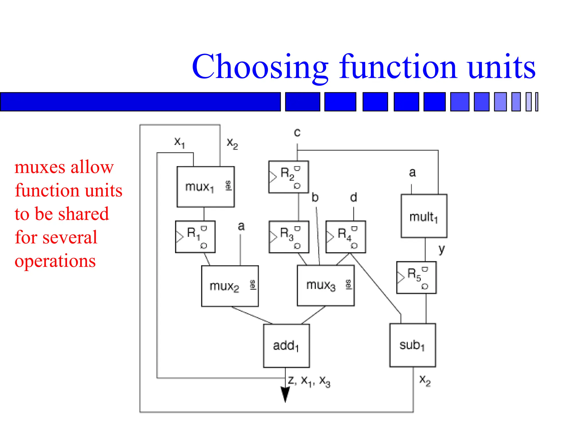
Allocation creates multiplexers
Same unit used for different values at
different times.
– Function units.
– Registers.
Multiplexer controls which value has access
to the unit.
Verilog for datapath
module dp(reset,clock,a,b,c,d,muxctrl1,muxctrl2,muxctrl3,
muxctrl4,loadr1,loadr2,loadr3,loadr4,x3,z);
parameter n=7;
input reset; input clock; input [n:0] a, b, c, d; // data primary inputs input muxctrl1, muxctrl2, muxctrl4; // mux control
input [1:0] muxctrl3; // 2-bit mux control input loadr1, loadr2, loadr3, loadr4; // register control output [n:0] x3, z;
reg [n:0] r1, r2, r3, r4; // registers
wire [n:0] mux1out, mux2out, mux3out, mux3bout, mux4out, mult1out, mult2out;
assign mux1out = (muxctrl1 == 0) ? a : r1;
assign mux2out = (muxctrl2 == 0) ? b : r4;
assign mux3out = (muxctrl3 == 0) ? a : (muxctrl3 == 1 ? r4 : r3);
assign mux4out = (muxctrl4 == 0) ? c : r2;
assign mult1out = mux1out * mux2out;
assign mult2out = mux3out * mux4out;
assign x3 = mult2out;
assign z = mult1out;
always @(posedge clock)
begin
if (reset)
r1 = 0; r2 = 0; r3 = 0; r4 = 0;
end
if (loadr1) r1 = mult1out;
if (loadr2) r2 = mult2out;
if (loadr3) r3 = c;
if (loadr4) r4 = d;
end
endmodule
27.
Choices during high-level
synthesis
Scheduling determines number of clock
cycles required; binding determines area,
cycle time.
Area tradeoffs must consider shared
function units vs. multiplexers, control.
Delay tradeoffs must consider cycle time
vs. number of cycles.
28.
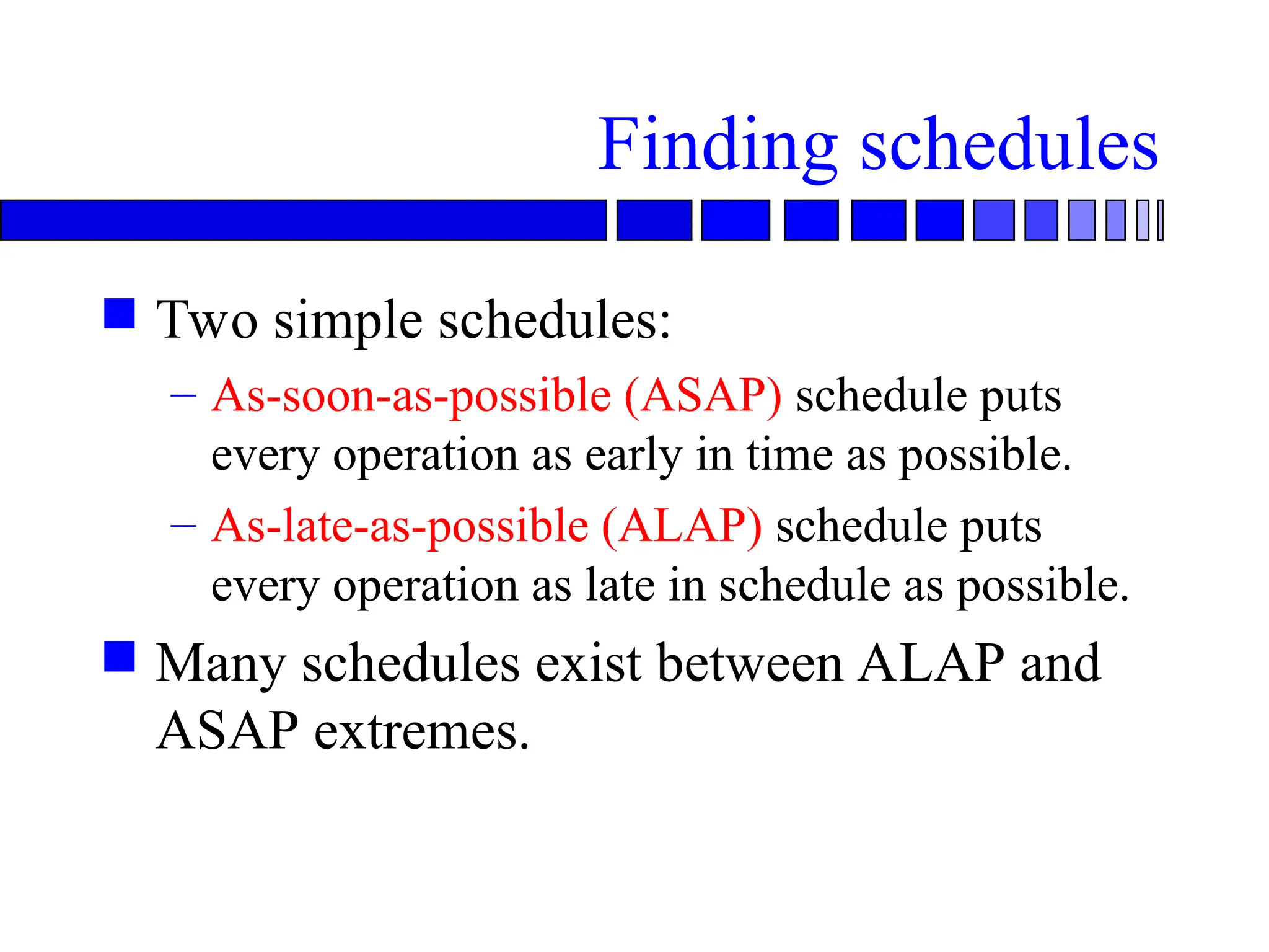
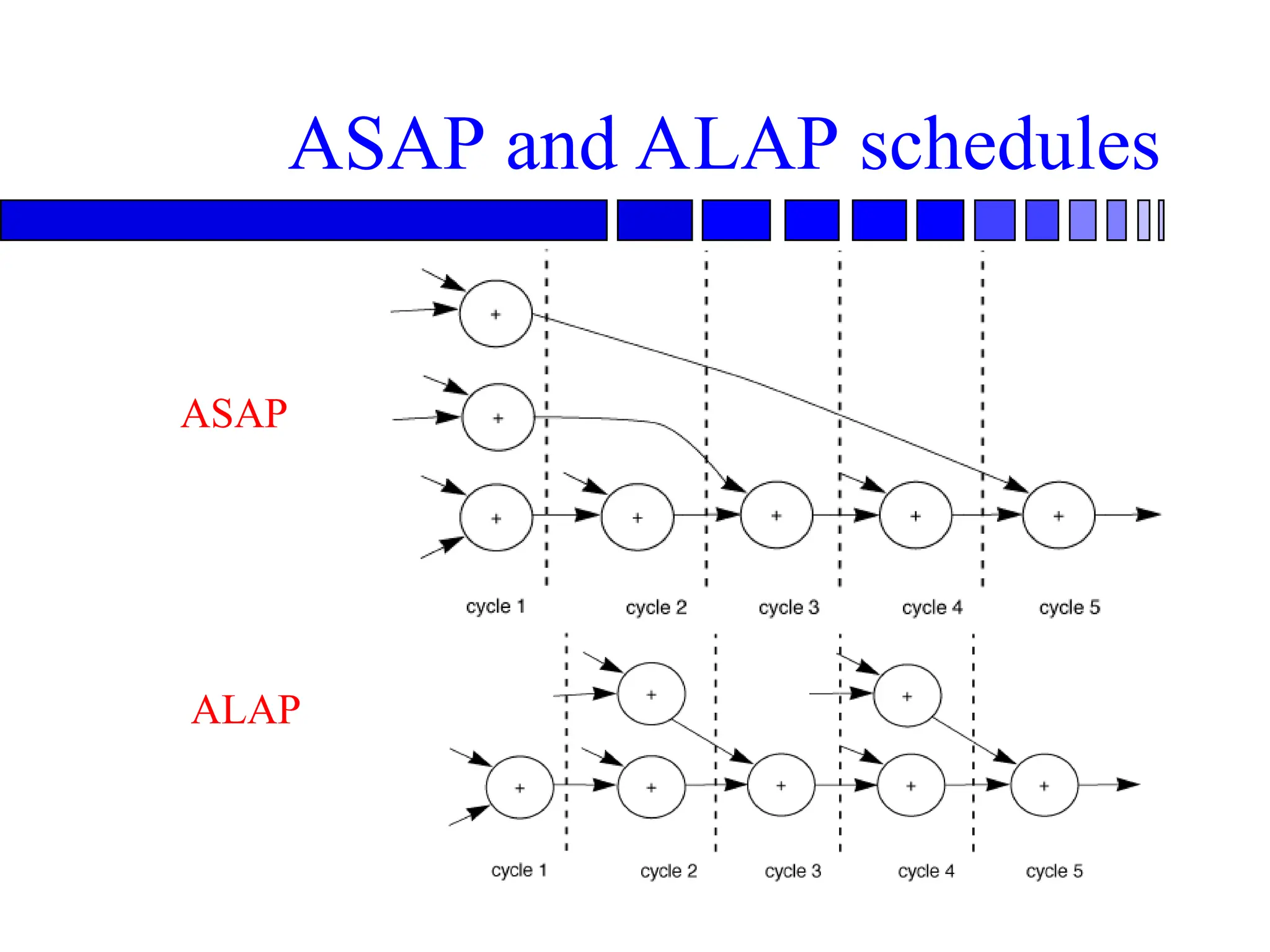
Finding schedules
Twosimple schedules:
– As-soon-as-possible (ASAP) schedule puts
every operation as early in time as possible.
– As-late-as-possible (ALAP) schedule puts
every operation as late in schedule as possible.
Many schedules exist between ALAP and
ASAP extremes.
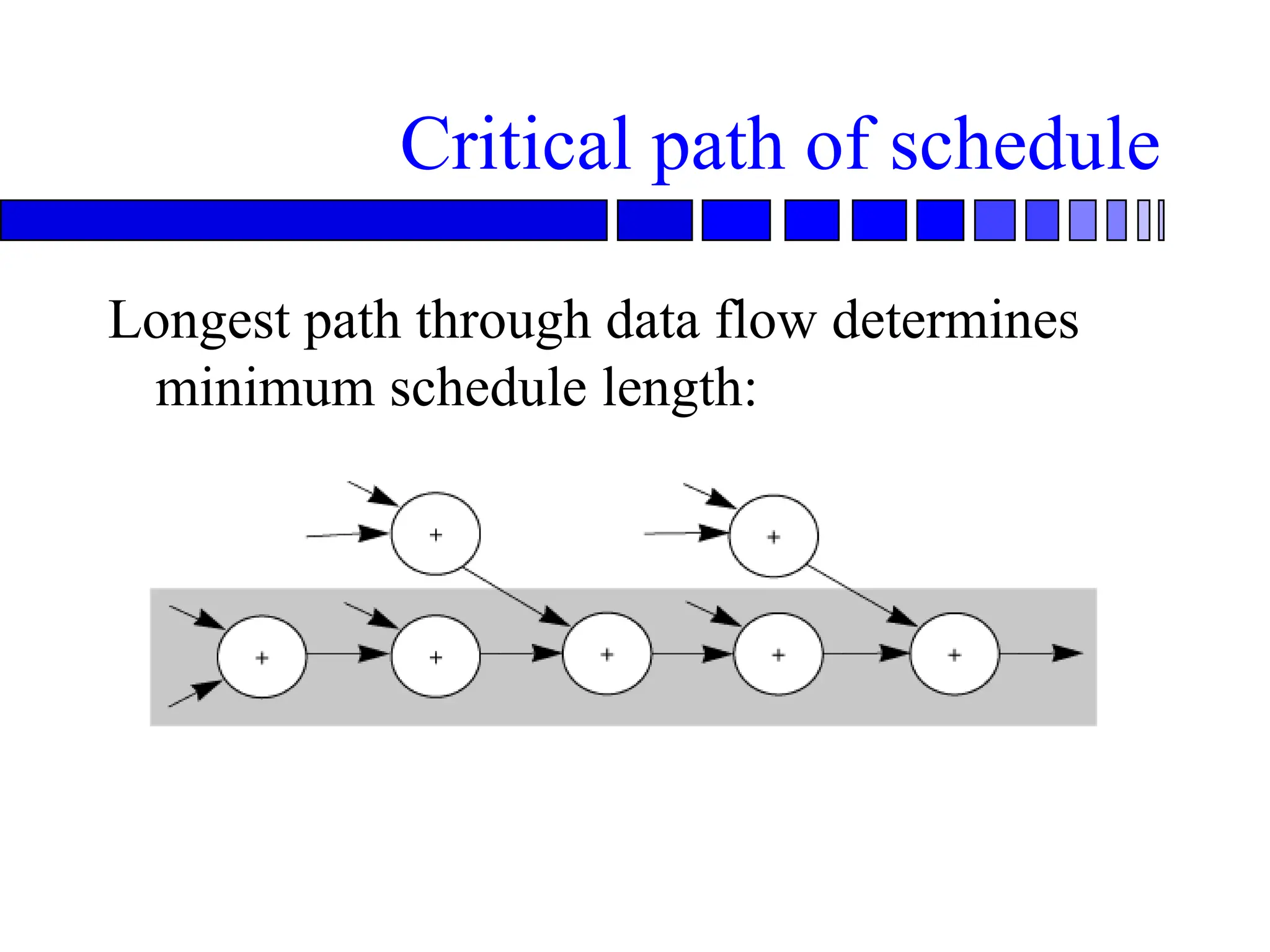
Critical path ofschedule
Longest path through data flow determines
minimum schedule length:
33.
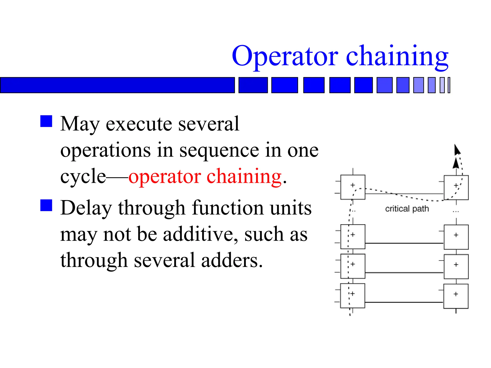
Operator chaining
Mayexecute several
operations in sequence in one
cycle—operator chaining.
Delay through function units
may not be additive, such as
through several adders.
34.
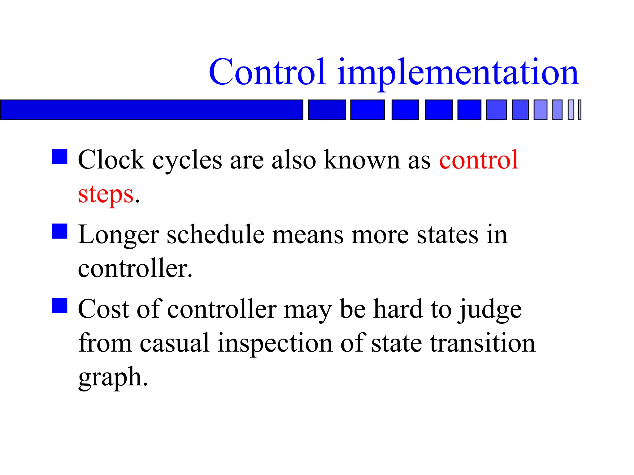
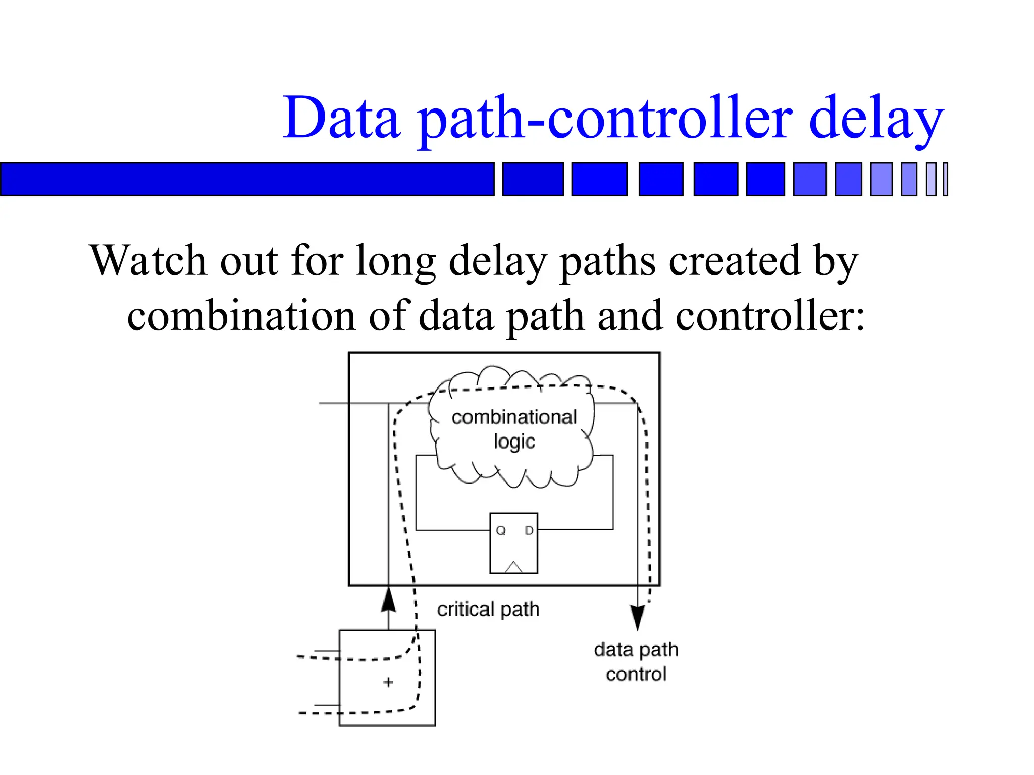
Control implementation
Clockcycles are also known as control
steps.
Longer schedule means more states in
controller.
Cost of controller may be hard to judge
from casual inspection of state transition
graph.
Hardwired vs. microcoded
control
Hardwired control has a state register and
“random logic.”
A microcoded machine has a state register
which points into a microcode memory.
Styles are equivalent; choice depends on
implementation considerations.
![Verilog for data path
module dp(reset,clock,a,b,c,d,muxctrl1,muxctrl2,muxctrl3,
muxctrl4,loadr1,loadr2,loadr3,loadr4,x3,z);
parameter n=7;
input reset; input clock; input [n:0] a, b, c, d; // data primary inputs input muxctrl1, muxctrl2, muxctrl4; // mux control
input [1:0] muxctrl3; // 2-bit mux control input loadr1, loadr2, loadr3, loadr4; // register control output [n:0] x3, z;
reg [n:0] r1, r2, r3, r4; // registers
wire [n:0] mux1out, mux2out, mux3out, mux3bout, mux4out, mult1out, mult2out;
assign mux1out = (muxctrl1 == 0) ? a : r1;
assign mux2out = (muxctrl2 == 0) ? b : r4;
assign mux3out = (muxctrl3 == 0) ? a : (muxctrl3 == 1 ? r4 : r3);
assign mux4out = (muxctrl4 == 0) ? c : r2;
assign mult1out = mux1out * mux2out;
assign mult2out = mux3out * mux4out;
assign x3 = mult2out;
assign z = mult1out;
always @(posedge clock)
begin
if (reset)
r1 = 0; r2 = 0; r3 = 0; r4 = 0;
end
if (loadr1) r1 = mult1out;
if (loadr2) r2 = mult2out;
if (loadr3) r3 = c;
if (loadr4) r4 = d;
end
endmodule](https://image.slidesharecdn.com/chapter6fpgadatapathcontroller-251115091335-07d0f2d2/75/Verilog-FPGA-data-path-controller-Design-Sequential-circuit-FSM-based-26-2048.jpg)
![Verilog model of ASAP schedule
reg [n-1:0] w1reg, w2reg, w6reg1, w6reg2, w6reg3,
w6reg4, w3reg1, w3reg2, w4reg, w5reg;
always @(posedge clock)
begin
// cycle 1
w1reg = i1 + i2;
w3reg1 = i4 + i5;
w6reg1 = i7 + i8;
// cycle 2
w2reg = w1reg + i3;
w3reg2 = w3reg1;
w6reg2 = w6reg1;
// cycle 3
w4reg = w3reg2 + w2reg;
w6reg3 = w6reg2;
// cycle 4
w5reg = i6 + w4reg;
w6reg4 = w6reg3;
// cycle 5
o1 = w6reg4 + w5reg;
end](https://image.slidesharecdn.com/chapter6fpgadatapathcontroller-251115091335-07d0f2d2/75/Verilog-FPGA-data-path-controller-Design-Sequential-circuit-FSM-based-30-2048.jpg)
![Verilog of ALAP schedule
reg [n-1:0] w1reg, w2reg, w6reg, w6reg2,
w6reg3, w3reg, w4reg, w5reg;
always @(posedge clock)
begin
// cycle 1
w1reg = i1 + i2;
// cycle 2
w2reg = w1reg + i3;
w3reg = i4 + i5;
// cycle 3
w4reg = w3reg + w2reg;
w6reg3 = w6reg2;
// cycle 4
w5reg = i6 + w4reg;
w6reg = i7 + i8;
// cycle 5
o1 = w6reg + w5reg;
end](https://image.slidesharecdn.com/chapter6fpgadatapathcontroller-251115091335-07d0f2d2/75/Verilog-FPGA-data-path-controller-Design-Sequential-circuit-FSM-based-31-2048.jpg)


![Verilog for data path
module dp(reset,clock,a,b,c,d,muxctrl1,muxctrl2,muxctrl3,
muxctrl4,loadr1,loadr2,loadr3,loadr4,x3,z);
parameter n=7;
input reset; input clock; input [n:0] a, b, c, d; // data primary inputs input muxctrl1, muxctrl2, muxctrl4; // mux control
input [1:0] muxctrl3; // 2-bit mux control input loadr1, loadr2, loadr3, loadr4; // register control output [n:0] x3, z;
reg [n:0] r1, r2, r3, r4; // registers
wire [n:0] mux1out, mux2out, mux3out, mux3bout, mux4out, mult1out, mult2out;
assign mux1out = (muxctrl1 == 0) ? a : r1;
assign mux2out = (muxctrl2 == 0) ? b : r4;
assign mux3out = (muxctrl3 == 0) ? a : (muxctrl3 == 1 ? r4 : r3);
assign mux4out = (muxctrl4 == 0) ? c : r2;
assign mult1out = mux1out * mux2out;
assign mult2out = mux3out * mux4out;
assign x3 = mult2out;
assign z = mult1out;
always @(posedge clock)
begin
if (reset)
r1 = 0; r2 = 0; r3 = 0; r4 = 0;
end
if (loadr1) r1 = mult1out;
if (loadr2) r2 = mult2out;
if (loadr3) r3 = c;
if (loadr4) r4 = d;
end
endmodule](https://crownmelresort.com/image.slidesharecdn.com/chapter6fpgadatapathcontroller-251115091335-07d0f2d2/75/Verilog-FPGA-data-path-controller-Design-Sequential-circuit-FSM-based-26-2048.jpg)


![Verilog model of ASAP schedule
reg [n-1:0] w1reg, w2reg, w6reg1, w6reg2, w6reg3,
w6reg4, w3reg1, w3reg2, w4reg, w5reg;
always @(posedge clock)
begin
// cycle 1
w1reg = i1 + i2;
w3reg1 = i4 + i5;
w6reg1 = i7 + i8;
// cycle 2
w2reg = w1reg + i3;
w3reg2 = w3reg1;
w6reg2 = w6reg1;
// cycle 3
w4reg = w3reg2 + w2reg;
w6reg3 = w6reg2;
// cycle 4
w5reg = i6 + w4reg;
w6reg4 = w6reg3;
// cycle 5
o1 = w6reg4 + w5reg;
end](https://crownmelresort.com/image.slidesharecdn.com/chapter6fpgadatapathcontroller-251115091335-07d0f2d2/75/Verilog-FPGA-data-path-controller-Design-Sequential-circuit-FSM-based-30-2048.jpg)
![Verilog of ALAP schedule
reg [n-1:0] w1reg, w2reg, w6reg, w6reg2,
w6reg3, w3reg, w4reg, w5reg;
always @(posedge clock)
begin
// cycle 1
w1reg = i1 + i2;
// cycle 2
w2reg = w1reg + i3;
w3reg = i4 + i5;
// cycle 3
w4reg = w3reg + w2reg;
w6reg3 = w6reg2;
// cycle 4
w5reg = i6 + w4reg;
w6reg = i7 + i8;
// cycle 5
o1 = w6reg + w5reg;
end](https://crownmelresort.com/image.slidesharecdn.com/chapter6fpgadatapathcontroller-251115091335-07d0f2d2/75/Verilog-FPGA-data-path-controller-Design-Sequential-circuit-FSM-based-31-2048.jpg)