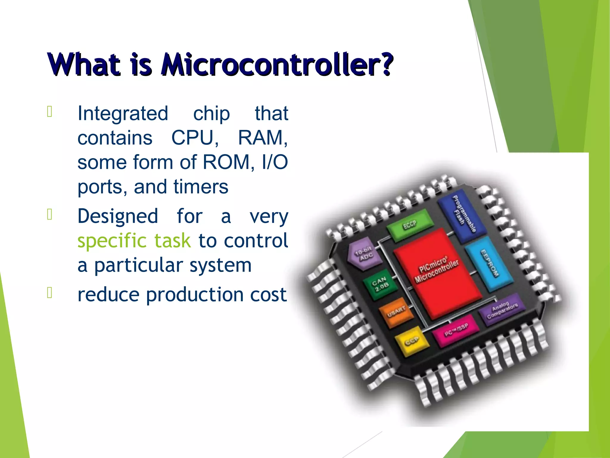
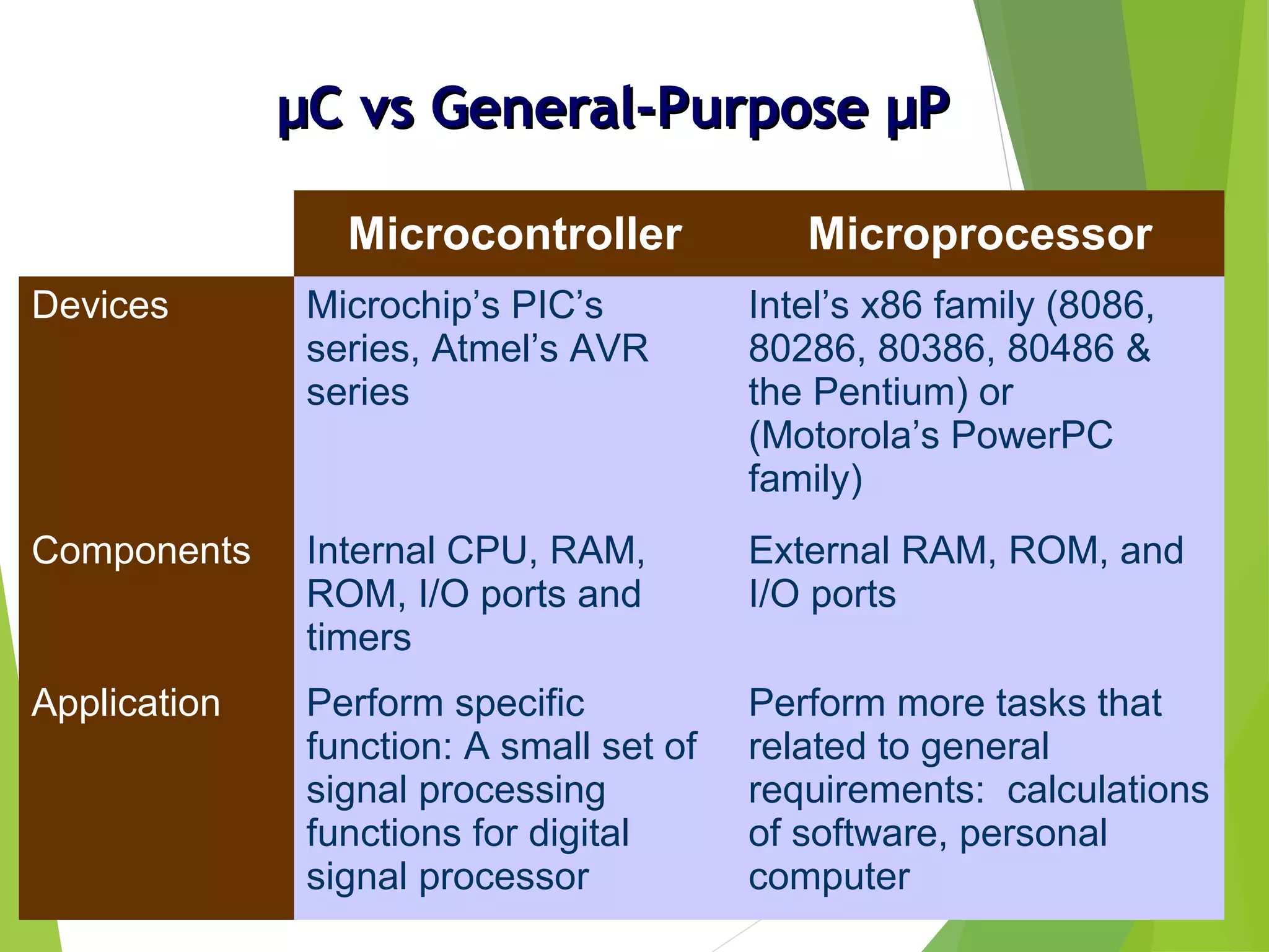
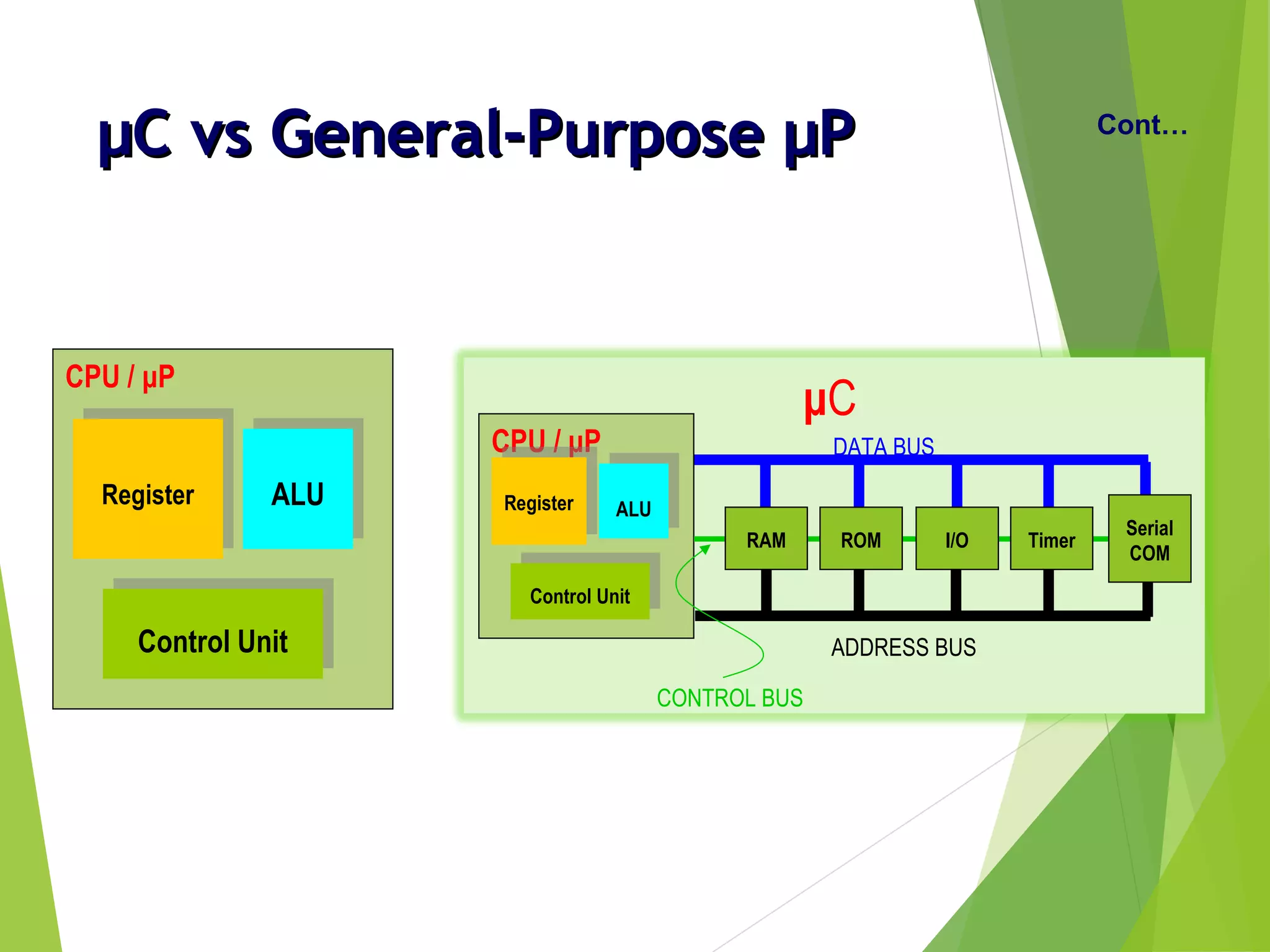
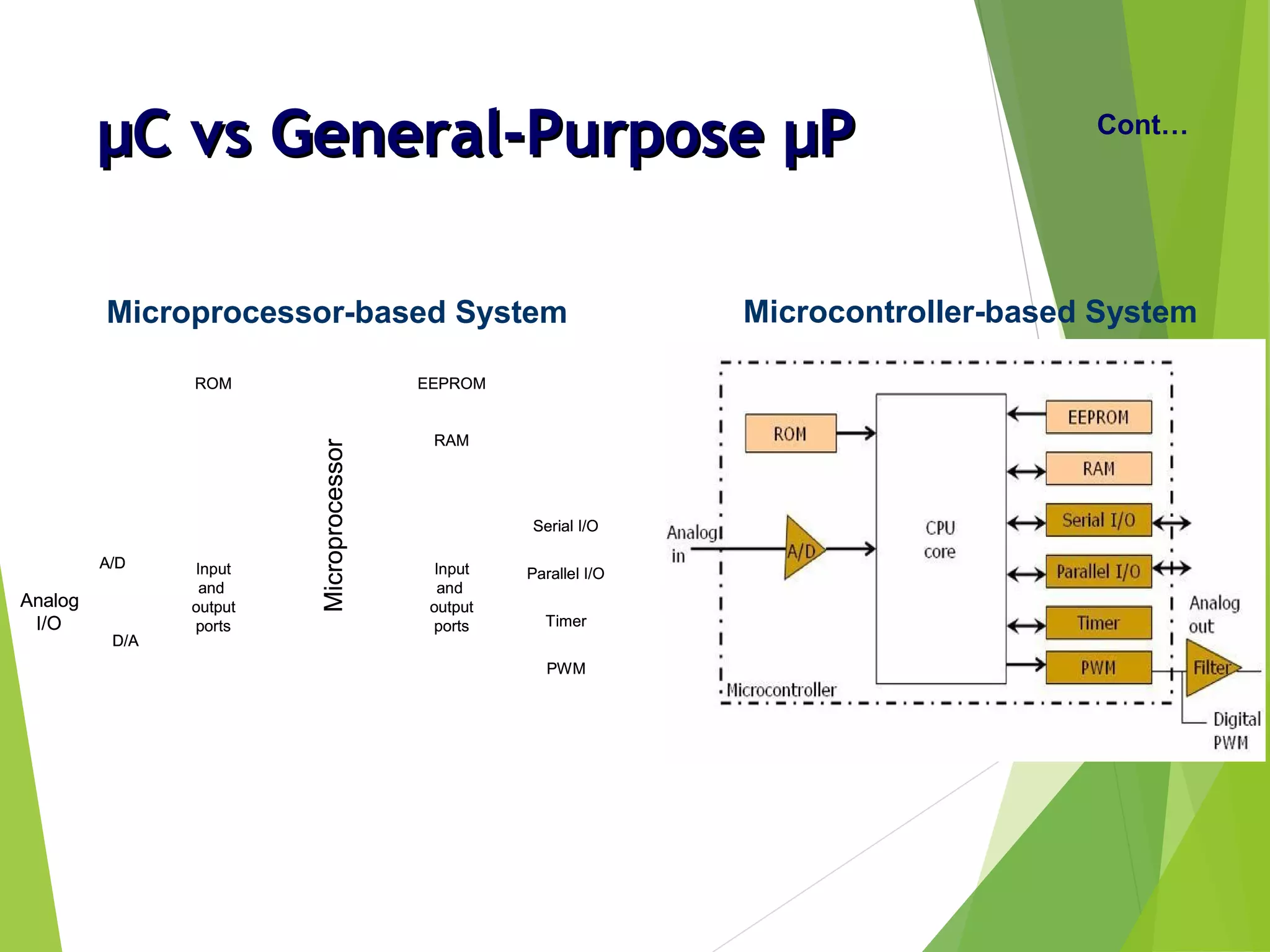
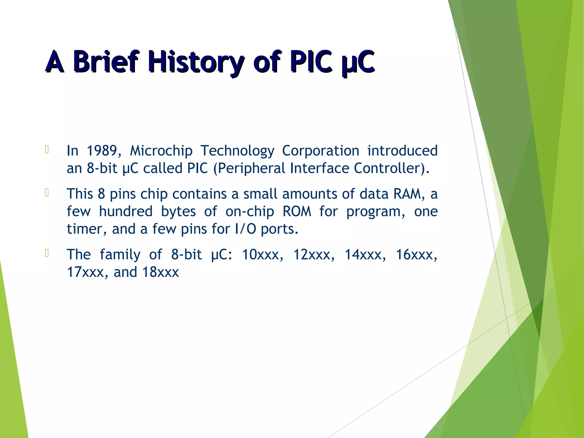
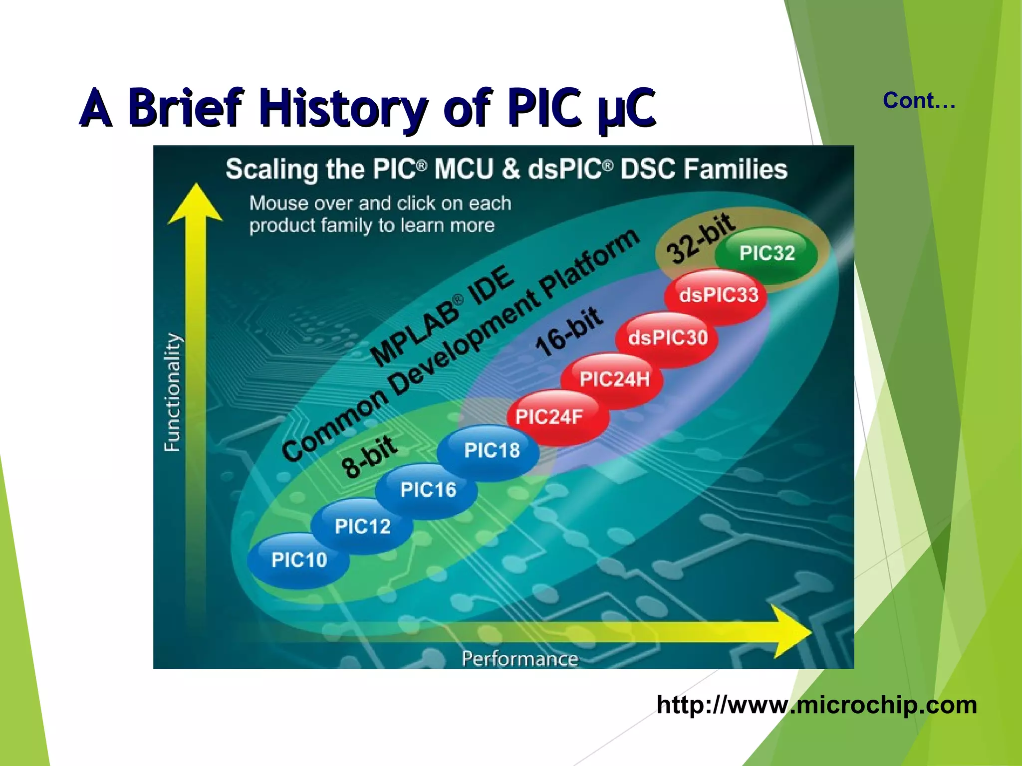
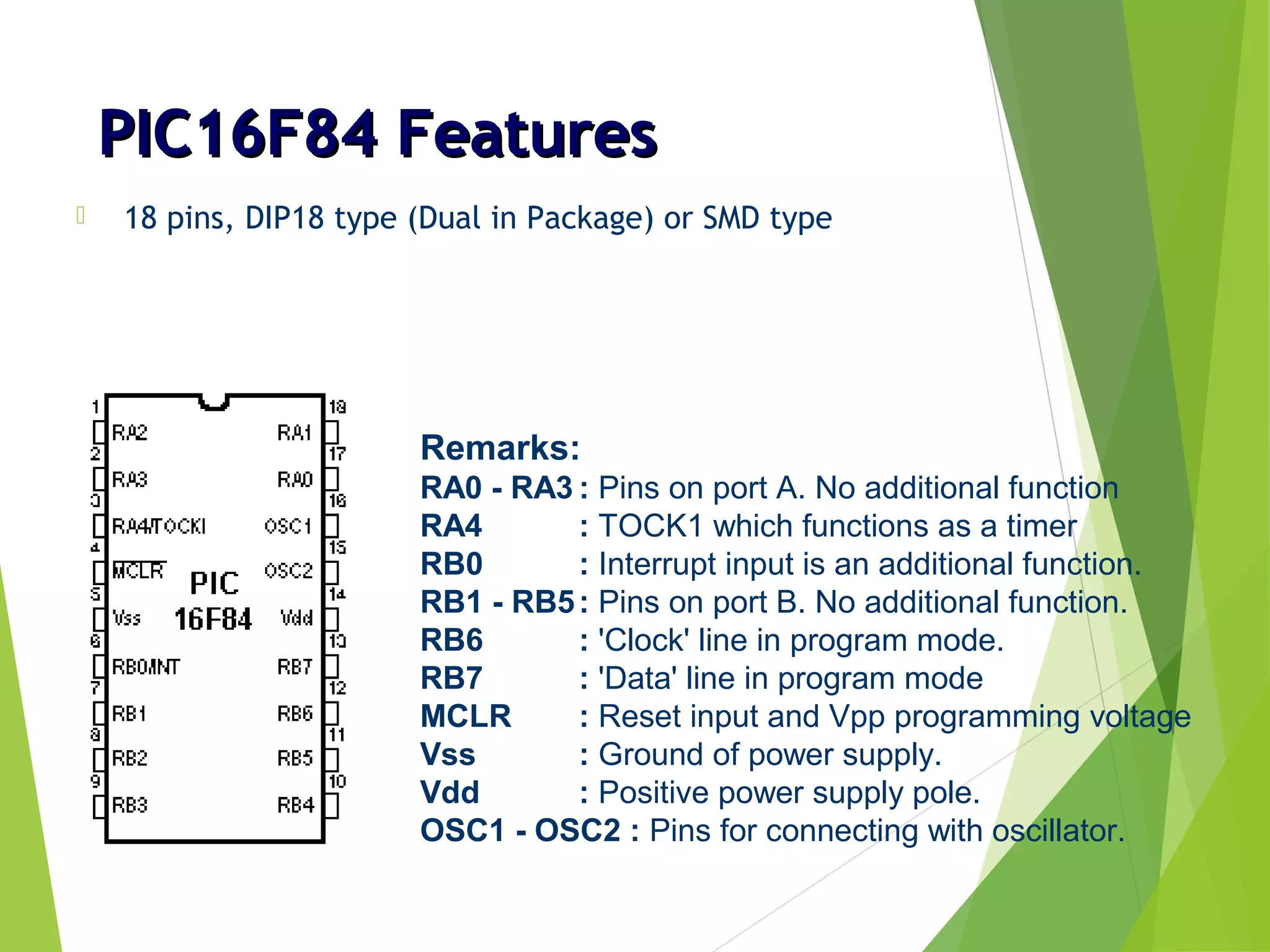
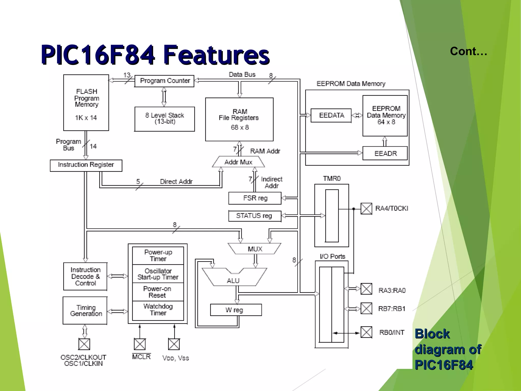
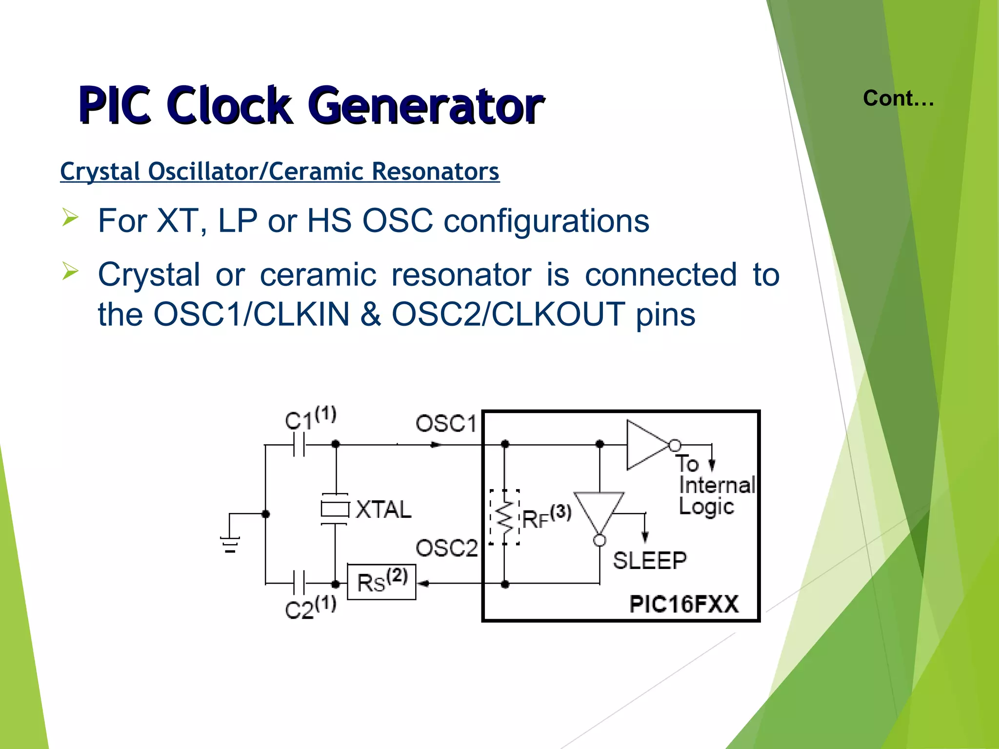
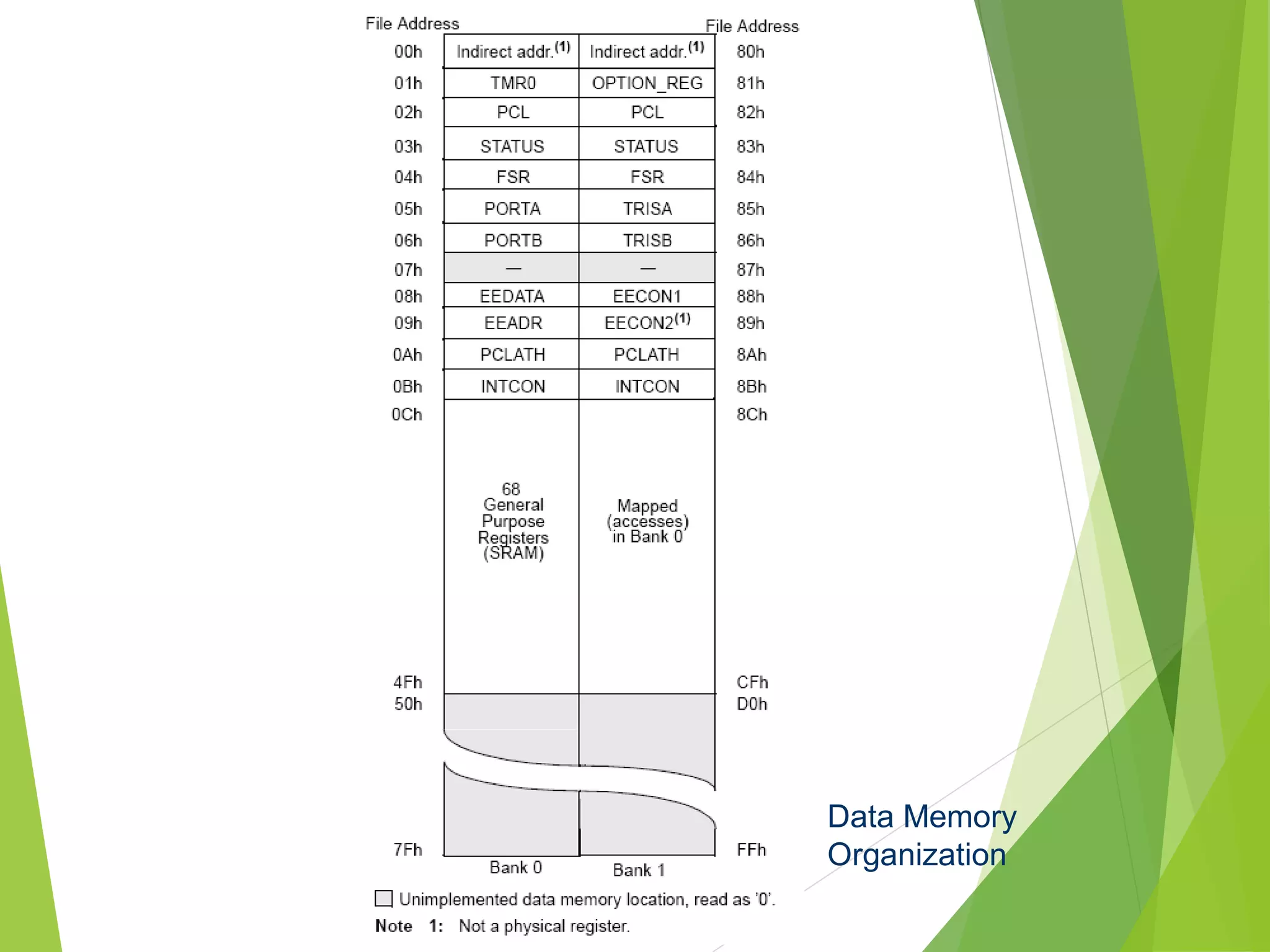
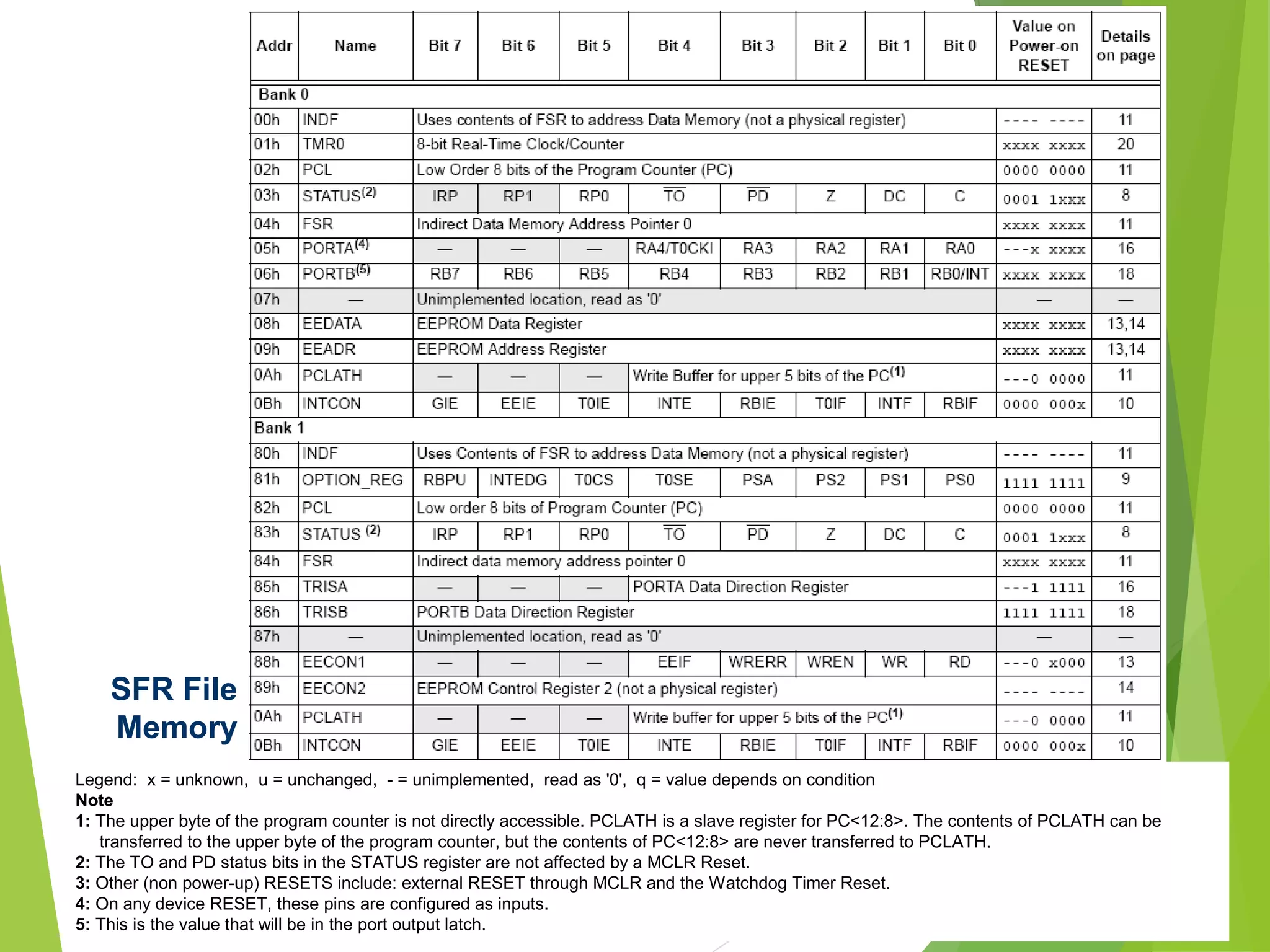
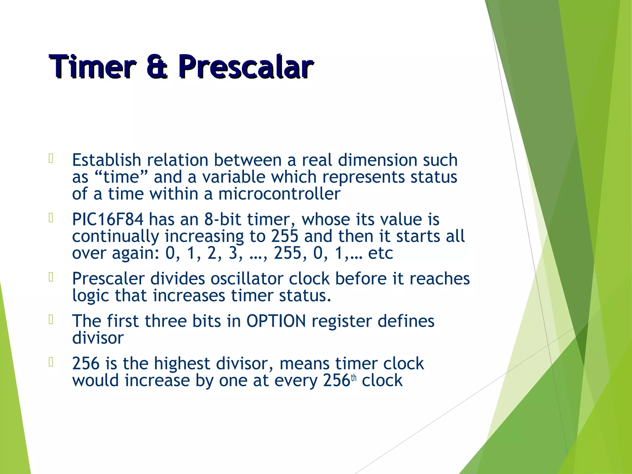
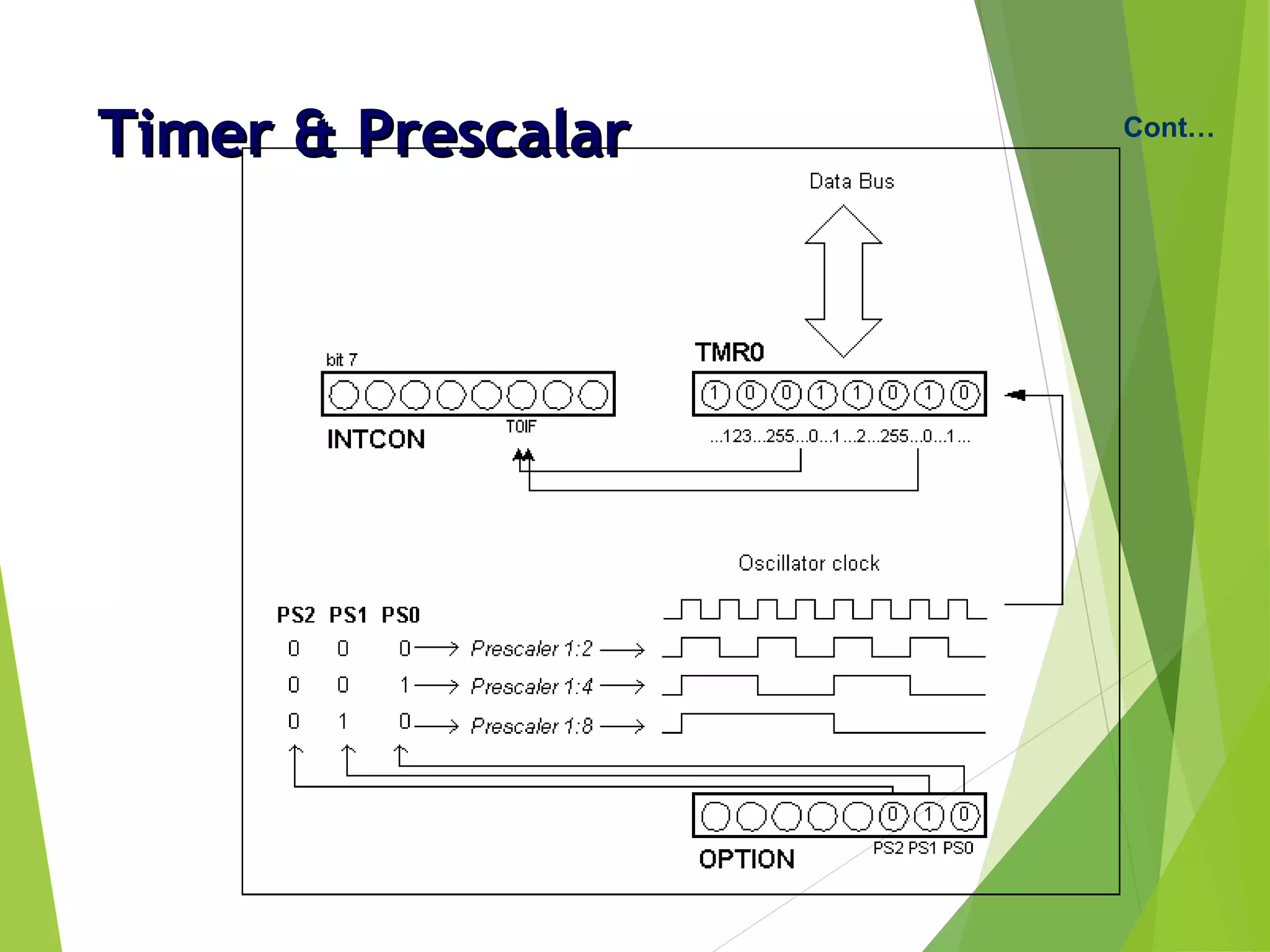
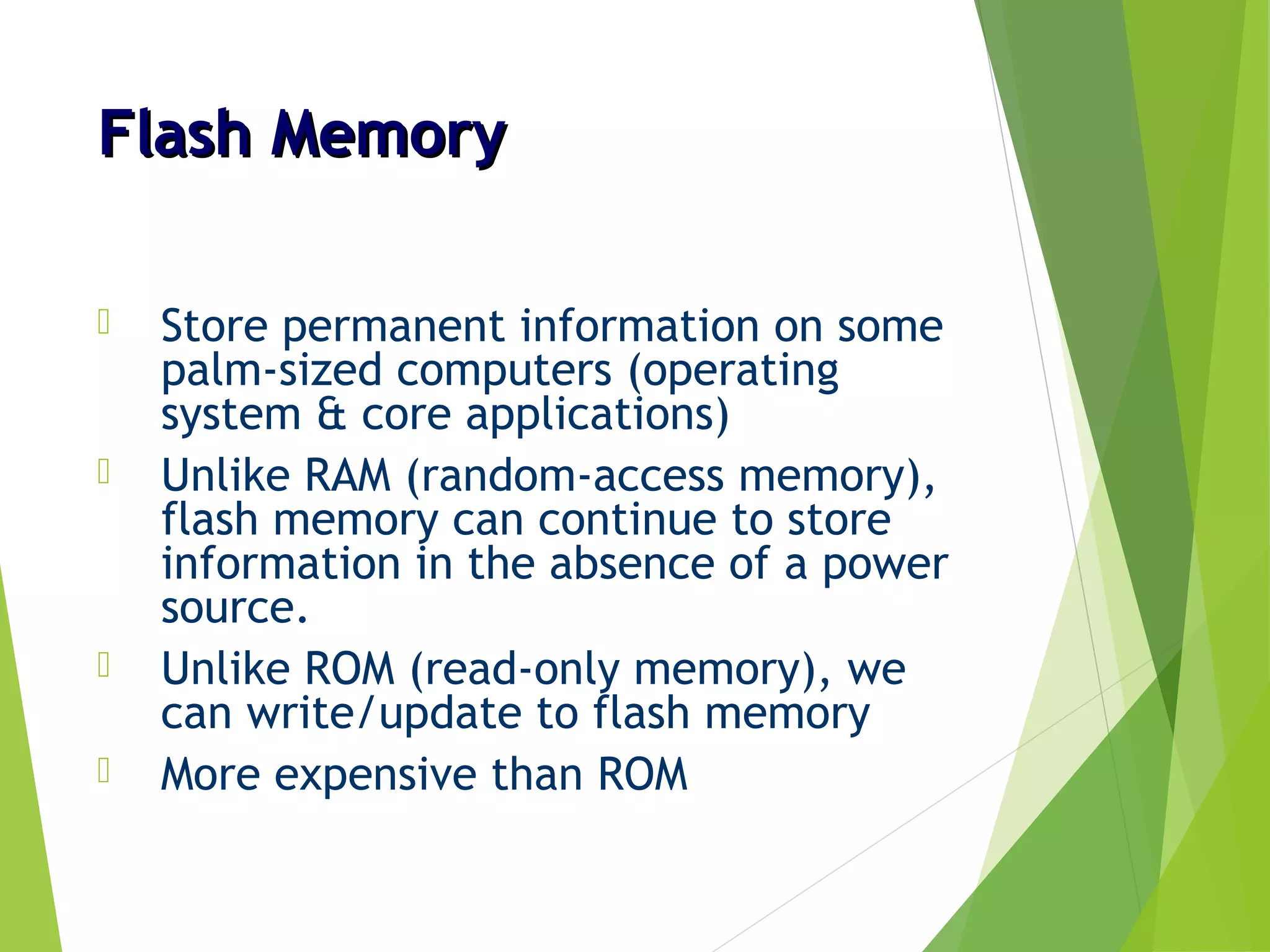
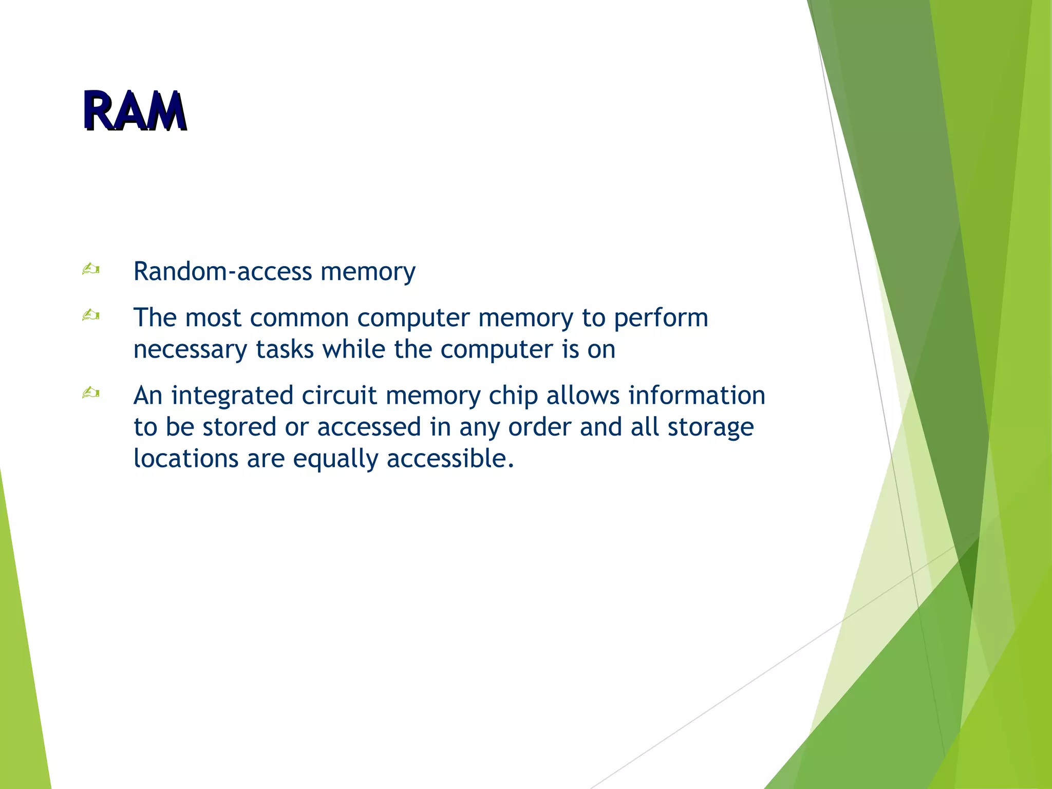
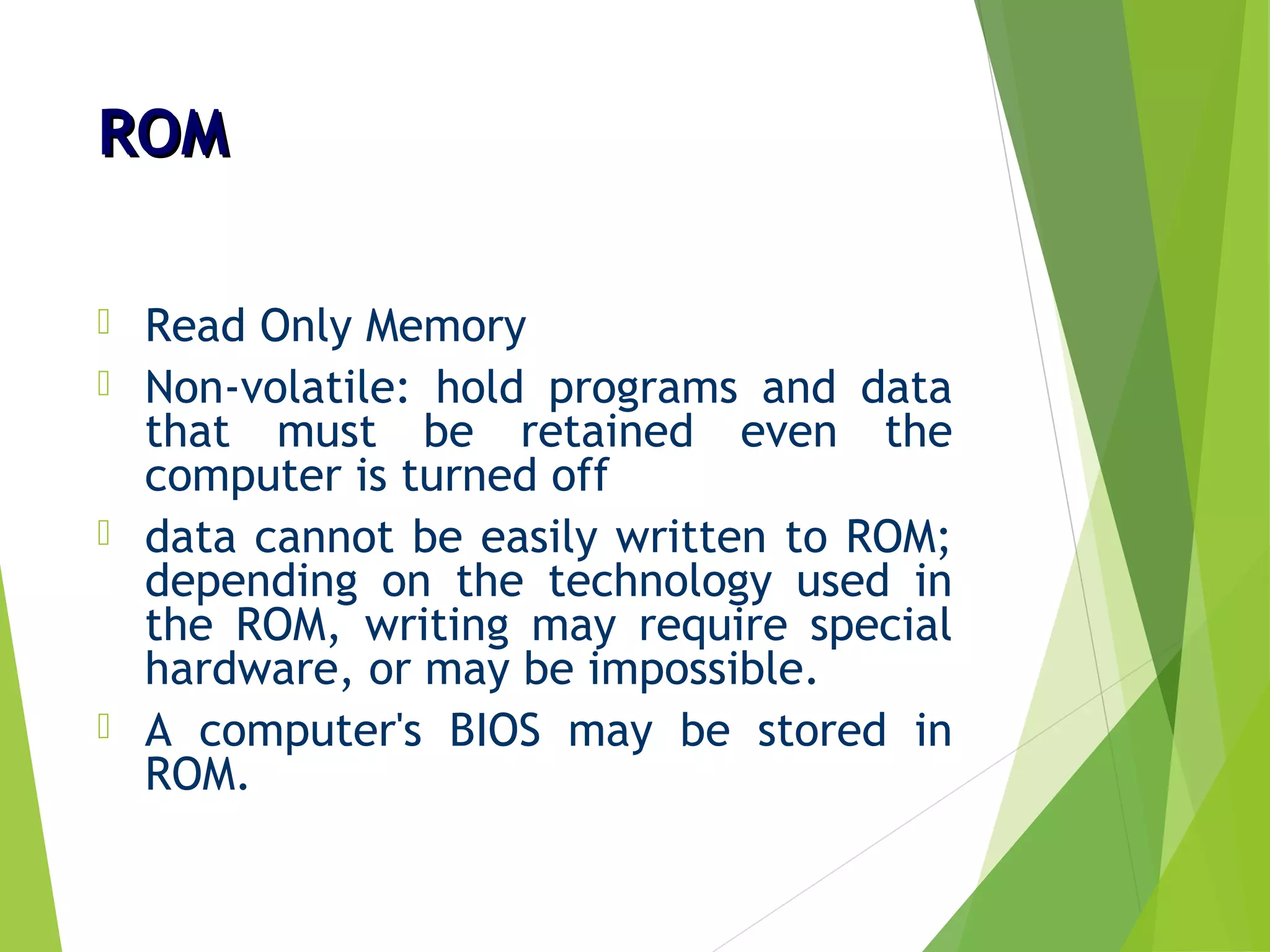
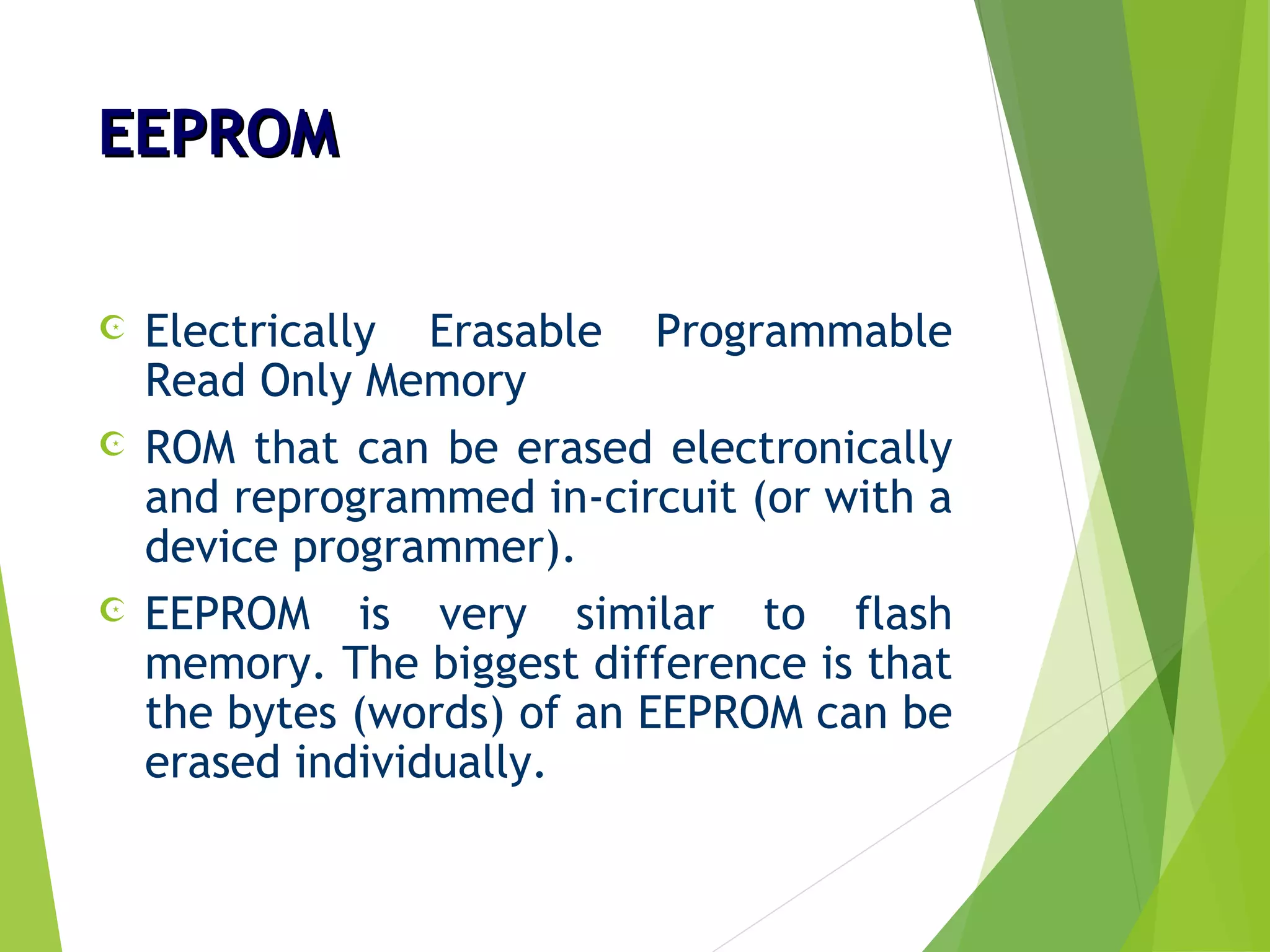
Introduction to theIntroduction to the
PIC MicrocontrollerPIC Microcontroller
OutlineOutline
 What is Microcontroller?
 µC vs General-Purpose µP
 A Brief History of PIC µC
 PIC16F84 Features
 PIC Clock Generator
 Reset
 PORTS
 Center Processing Unit (CPU)
 MEMORY ORGANIZATION
 Timer & Prescalar
 Flash Memory
 RAM
 ROM
 EEPROM
What is Microcontroller?What is Microcontroller?
 Integrated chip that
contains CPU, RAM,
some form of ROM, I/O
ports, and timers
 Designed for a very
specific task to control
a particular system
 reduce production cost
µCµC vs General-Purposevs General-Purpose µµPP
Microcontroller Microprocessor
Devices Microchip’s PIC’s
series, Atmel’s AVR
series
Intel’s x86 family (8086,
80286, 80386, 80486 &
the Pentium) or
(Motorola’s PowerPC
family)
Components Internal CPU, RAM,
ROM, I/O ports and
timers
External RAM, ROM, and
I/O ports
Application Perform specific
function: A small set of
signal processing
functions for digital
signal processor
Perform more tasks that
related to general
requirements: calculations
of software, personal
computer
µCµC vs General-Purposevs General-Purpose µµPP Cont…
CPU / μP
RegisterRegister
Control UnitControl Unit
ALUALU
DATA BUSCPU / μP
Register
Register
Control Unit
Control Unit
ALU
ALU
ADDRESS BUS
CONTROL BUS
μC
RAM ROM I/O Timer
Serial
COM
µCµC vs General-Purposevs General-Purpose µµPP Cont…
Microprocessor
EEPROM
RAM
Input
and
output
ports
Serial I/O
Parallel I/O
Timer
PWM
Input
and
output
ports
A/D
D/A
Analog
I/O
ROM
Microprocessor
EEPROM
RAM
Input
and
output
ports
Serial I/O
Parallel I/O
Timer
PWM
Input
and
output
ports
A/DA/D
D/AD/A
Analog
I/O
ROM
Microprocessor-based System Microcontroller-based System
A Brief History of PIC µCA Brief History of PIC µC
 In 1989, Microchip Technology Corporation introduced
an 8-bit µC called PIC (Peripheral Interface Controller).
 This 8 pins chip contains a small amounts of data RAM, a
few hundred bytes of on-chip ROM for program, one
timer, and a few pins for I/O ports.
 The family of 8-bit µC: 10xxx, 12xxx, 14xxx, 16xxx,
17xxx, and 18xxx
A Brief History of PIC µCA Brief History of PIC µC Cont…
http://www.microchip.com
A Brief History of PIC µCA Brief History of PIC µC
 They are all 8-bit processors that the CPU can work on
only 8 bits of data a time.
 Problem: not all 100% upwardly compatible in terms of
software when going from one family to another family.
 Ex.: 12xxx - 12-bit wide instructions
16xxx- 14-bit wide instructions
PIC18xxx - 16-bit wide with many
new instructions
Cont…
A Brief History of PIC µCA Brief History of PIC µC
Advantages of PIC:
 30 to 100 times faster than other µCs (program memory is
integrated to the chip)
 Smaller size (on-board memory)
 Easy to program, reusable and inexpensive
Cont…
A Brief History of PIC µCA Brief History of PIC µC
Architecture:
Cont…
CPU
Program &
Data Memory
Von Neumann architecture
CPU
Program
Memory
Data
Memory
Harvard architecture
PIC16F84 FeaturesPIC16F84 Features
 18 pins, DIP18 type (Dual in Package) or SMD type
Remarks:
RA0 - RA3 : Pins on port A. No additional function
RA4 : TOCK1 which functions as a timer
RB0 : Interrupt input is an additional function.
RB1 - RB5: Pins on port B. No additional function.
RB6 : 'Clock' line in program mode.
RB7 : 'Data' line in program mode
MCLR : Reset input and Vpp programming voltage
Vss : Ground of power supply.
Vdd : Positive power supply pole.
OSC1 - OSC2 : Pins for connecting with oscillator.
PIC16F84 FeaturesPIC16F84 Features Cont…
BlockBlock
diagram ofdiagram of
PIC16F84PIC16F84
PIC Clock GeneratorPIC Clock Generator
 To provide a clock for executing a program or program
instructions of µC.
 Types of PIC clock generator:
 A crystal & two capacitors
 Resonators or external resistor-capacitor pair
 Built-in resistor-capacitor
PIC Clock GeneratorPIC Clock Generator
 PIC16F84 can operate in four different oscillation
modes:
- LP low power crystal
- XT crystal/resonator
- HS high speed crystal/resonator
- RC resistor/capacitor
 Two configuration bits, FOSC1 & FOSC0 are used to
select one of these four modes
Cont…
PIC Clock GeneratorPIC Clock Generator
Crystal Oscillator/Ceramic Resonators
 For XT, LP or HS OSC configurations
 Crystal or ceramic resonator is connected to
the OSC1/CLKIN & OSC2/CLKOUT pins
Cont…
PIC Clock GeneratorPIC Clock Generator
 A parallel cut crystal is used to design PIC16F84A
 The use of a series cut crystal may give a freq. out of the crystal
manufacturer’s specifications
Cont…
External clock input operations
PIC Clock GeneratorPIC Clock Generator Cont…
Capacitor selection for ceramic resonators
Capacitor selection for crystal resonators
PIC Clock GeneratorPIC Clock Generator
RC Oscillator
 Reduce cost for timing insensitive applications
 Variation of the oscillator frequency:
- operating temperature
- process parameter variation
- difference in lead frame capacitance between package types (low
CEXT values)
- tolerance of the external R & C components
Cont…
ResetReset
 Power-on Reset (POR)
 MCLR during normal operation
 MCLR during SLEEP
 WDT Reset (during normal
operation)
 WDT Wake-up (during SLEEP)
Register Reset value (hex)
PC 000000
WREG 00
SP 00
TRISA-TRISB FF
Value registers upon reset
PORTSPORTS
 Physical connection of CPU and outside world – monitor
@ control other components @ devices
 A group of pins which can be accessed simultaneously @
set the desired combination of zeros and ones
 All port pins can be designated as input @ output
PORTS:PORTS: PORTA & TRISAPORTA & TRISA
 PORTA is a 5-bit wide, bi-directional port
 TRISA: data direction register of PORTA
 TRISA = 1, PORTA is
an input (output
driver in HI-
impedance mode)
 TRISA = 0, PORTA is
an output (contents
of the output latch
on the selected pin)
PORTS:PORTS: PORTB & TRISBPORTB & TRISB
 PORTB is a 8-bit wide, bi-directional port
 TRISB: data direction register of PORTB
 TRISB = 1, PORTB
is an input (output
driver in HI-
impedance mode)
 TRISB = 0, PORTB
is an output
(contents of the
output latch on the
selected pin)
Center Processing UnitCenter Processing Unit
(CPU)(CPU) The brain of the µC
 Connect all parts of the µC through a data bus
& and an address bus
 Find, fetch, decode & execute the right
instruction
 CPU resources:
 Registers: store temporary information
 ALU: performing arithmetic functions
 Program counter: point to the address of the next
instruction to be executed
 Instruction decoder: interpret the instruction
fetched into the CPU
Center Processing UnitCenter Processing Unit
(CPU)(CPU)
MOVLW 0x20
Program
Memory
Temporary
storage
executeexecute
Memory
11 00xx 0010 0000
opcode
Assembler (translator)
Decoder
Fetch
instruction
Fetch
instruction
Center Processing UnitCenter Processing Unit
(CPU)(CPU)
Arithmetic Logic Unit (ALU)
 Add, subtract, move (left @ right within a register)
and logic operations
 PIC16F84 contains an 8-bit ALU & 8-bit working
registers (WREG)
 ALU instructions: two operands @ one operand
 Two operands: WREG + file register @ immediate
constant
 Registers: GPR (General Purposes Registers) & SFP
(Special Function Registers)
 One operand: WREG @ a file register
 Execution of ALU instructions can affect STATUS bits
which are carry (C), digit carry (DC), and zero (Z).
Cont…
Center Processing UnitCenter Processing Unit
(CPU)(CPU)
Cont…
ALU
STATUS
register
8-bit literal (from
instruction word)
WREG
register
8-
bit
8-
bit
8-bit
Z, DC, C flags
Carry bit
MEMORY ORGANIZATIONMEMORY ORGANIZATION
 PIC16F84 has two separate memory blocks: data &
program
 Data block: GPR and SFP registers in RAM memory
(read/write memory- static memory), EEPROM memory
 Program block: FLASH memory
Memory
organization
of PIC16F84
MEMORY ORGANIZATION:MEMORY ORGANIZATION: Program MemoryProgram Memory
 Used for storing programs (opcodes), directly
under control of program counter (PC)
 Wake up memory (address 0000H) when PIC is
powered up.
 Has been carried out in FLASH technology
(indicated by the letter F in the part number, C for
one-time programmable (OTP)): possible to
program a µC many times
 Size of 1024 locations, 14 bits width
 Locations 0000h & 0004h are reserved for
reset & interrupt vector, respectively
 The 1st
1Kx14 (0000h-03FFh) are physically
implemented address
 Accessing a location of physically
implemented address will cause a wraparound
MEMORY ORGANIZATION:MEMORY ORGANIZATION: Program MemoryProgram Memory
MEMORY ORGANIZATION:MEMORY ORGANIZATION: Data MemoryData Memory
 Also known as file register: data storage, scratch pad & registers for internal use and
functions
 Special Function Registers (SFR)
- 8-bit wide
- ALU status, timers, serial communication, I/O ports, ADC, & etc.
- function of each SFR is fixed in design, used to control µC or peripheral
- access either directly (names @ addresses) or indirectly (FSR – File Select
Register)
- classified into core and peripheral sets
- control bits (RP1, RP0) in STATUS register are used for bank selection
 General Purpose Registers (GPR)
- 8-bit wide
- also called general purpose RAM (GP RAM)
- used for data storage & scratch pad
- accessed directly
- addresses in Bank 0 & Bank 1 are mapped together
 Location of SFR and GPR vary from chip to chip, even among members of the
same family
Data Memory
Organization
SFR File
Memory
Legend: x = unknown, u = unchanged, - = unimplemented, read as '0', q = value depends on condition
Note
1: The upper byte of the program counter is not directly accessible. PCLATH is a slave register for PC<12:8>. The contents of PCLATH can be
transferred to the upper byte of the program counter, but the contents of PC<12:8> are never transferred to PCLATH.
2: The TO and PD status bits in the STATUS register are not affected by a MCLR Reset.
3: Other (non power-up) RESETS include: external RESET through MCLR and the Watchdog Timer Reset.
4: On any device RESET, these pins are configured as inputs.
5: This is the value that will be in the port output latch.
Timer & PrescalarTimer & Prescalar
 Establish relation between a real dimension such
as “time” and a variable which represents status
of a time within a microcontroller
 PIC16F84 has an 8-bit timer, whose its value is
continually increasing to 255 and then it starts all
over again: 0, 1, 2, 3, …, 255, 0, 1,… etc
 Prescaler divides oscillator clock before it reaches
logic that increases timer status.
 The first three bits in OPTION register defines
divisor
 256 is the highest divisor, means timer clock
would increase by one at every 256th
clock
Timer & PrescalarTimer & Prescalar Cont…
Flash MemoryFlash Memory
 Store permanent information on some
palm-sized computers (operating
system & core applications)
 Unlike RAM (random-access memory),
flash memory can continue to store
information in the absence of a power
source.
 Unlike ROM (read-only memory), we
can write/update to flash memory
 More expensive than ROM
RAMRAM
 Random-access memory
 The most common computer memory to perform
necessary tasks while the computer is on
 An integrated circuit memory chip allows information
to be stored or accessed in any order and all storage
locations are equally accessible.
ROMROM
 Read Only Memory
 Non-volatile: hold programs and data
that must be retained even the
computer is turned off
 data cannot be easily written to ROM;
depending on the technology used in
the ROM, writing may require special
hardware, or may be impossible.
 A computer's BIOS may be stored in
ROM.
EEPROMEEPROM
 Electrically Erasable Programmable
Read Only Memory
 ROM that can be erased electronically
and reprogrammed in-circuit (or with a
device programmer).
 EEPROM is very similar to flash
memory. The biggest difference is that
the bytes (words) of an EEPROM can be
erased individually.
PIC Introduction and explained in detailed

PIC Introduction and explained in detailed

  • 1.
    Introduction to theIntroductionto the PIC MicrocontrollerPIC Microcontroller
  • 2.
    OutlineOutline  What isMicrocontroller?  µC vs General-Purpose µP  A Brief History of PIC µC  PIC16F84 Features  PIC Clock Generator  Reset  PORTS  Center Processing Unit (CPU)  MEMORY ORGANIZATION  Timer & Prescalar  Flash Memory  RAM  ROM  EEPROM
  • 3.
    What is Microcontroller?Whatis Microcontroller?  Integrated chip that contains CPU, RAM, some form of ROM, I/O ports, and timers  Designed for a very specific task to control a particular system  reduce production cost
  • 4.
    µCµC vs General-PurposevsGeneral-Purpose µµPP Microcontroller Microprocessor Devices Microchip’s PIC’s series, Atmel’s AVR series Intel’s x86 family (8086, 80286, 80386, 80486 & the Pentium) or (Motorola’s PowerPC family) Components Internal CPU, RAM, ROM, I/O ports and timers External RAM, ROM, and I/O ports Application Perform specific function: A small set of signal processing functions for digital signal processor Perform more tasks that related to general requirements: calculations of software, personal computer
  • 5.
    µCµC vs General-PurposevsGeneral-Purpose µµPP Cont… CPU / μP RegisterRegister Control UnitControl Unit ALUALU DATA BUSCPU / μP Register Register Control Unit Control Unit ALU ALU ADDRESS BUS CONTROL BUS μC RAM ROM I/O Timer Serial COM
  • 6.
    µCµC vs General-PurposevsGeneral-Purpose µµPP Cont… Microprocessor EEPROM RAM Input and output ports Serial I/O Parallel I/O Timer PWM Input and output ports A/D D/A Analog I/O ROM Microprocessor EEPROM RAM Input and output ports Serial I/O Parallel I/O Timer PWM Input and output ports A/DA/D D/AD/A Analog I/O ROM Microprocessor-based System Microcontroller-based System
  • 7.
    A Brief Historyof PIC µCA Brief History of PIC µC  In 1989, Microchip Technology Corporation introduced an 8-bit µC called PIC (Peripheral Interface Controller).  This 8 pins chip contains a small amounts of data RAM, a few hundred bytes of on-chip ROM for program, one timer, and a few pins for I/O ports.  The family of 8-bit µC: 10xxx, 12xxx, 14xxx, 16xxx, 17xxx, and 18xxx
  • 8.
    A Brief Historyof PIC µCA Brief History of PIC µC Cont… http://www.microchip.com
  • 9.
    A Brief Historyof PIC µCA Brief History of PIC µC  They are all 8-bit processors that the CPU can work on only 8 bits of data a time.  Problem: not all 100% upwardly compatible in terms of software when going from one family to another family.  Ex.: 12xxx - 12-bit wide instructions 16xxx- 14-bit wide instructions PIC18xxx - 16-bit wide with many new instructions Cont…
  • 10.
    A Brief Historyof PIC µCA Brief History of PIC µC Advantages of PIC:  30 to 100 times faster than other µCs (program memory is integrated to the chip)  Smaller size (on-board memory)  Easy to program, reusable and inexpensive Cont…
  • 11.
    A Brief Historyof PIC µCA Brief History of PIC µC Architecture: Cont… CPU Program & Data Memory Von Neumann architecture CPU Program Memory Data Memory Harvard architecture
  • 12.
    PIC16F84 FeaturesPIC16F84 Features 18 pins, DIP18 type (Dual in Package) or SMD type Remarks: RA0 - RA3 : Pins on port A. No additional function RA4 : TOCK1 which functions as a timer RB0 : Interrupt input is an additional function. RB1 - RB5: Pins on port B. No additional function. RB6 : 'Clock' line in program mode. RB7 : 'Data' line in program mode MCLR : Reset input and Vpp programming voltage Vss : Ground of power supply. Vdd : Positive power supply pole. OSC1 - OSC2 : Pins for connecting with oscillator.
  • 13.
    PIC16F84 FeaturesPIC16F84 FeaturesCont… BlockBlock diagram ofdiagram of PIC16F84PIC16F84
  • 14.
    PIC Clock GeneratorPICClock Generator  To provide a clock for executing a program or program instructions of µC.  Types of PIC clock generator:  A crystal & two capacitors  Resonators or external resistor-capacitor pair  Built-in resistor-capacitor
  • 15.
    PIC Clock GeneratorPICClock Generator  PIC16F84 can operate in four different oscillation modes: - LP low power crystal - XT crystal/resonator - HS high speed crystal/resonator - RC resistor/capacitor  Two configuration bits, FOSC1 & FOSC0 are used to select one of these four modes Cont…
  • 16.
    PIC Clock GeneratorPICClock Generator Crystal Oscillator/Ceramic Resonators  For XT, LP or HS OSC configurations  Crystal or ceramic resonator is connected to the OSC1/CLKIN & OSC2/CLKOUT pins Cont…
  • 17.
    PIC Clock GeneratorPICClock Generator  A parallel cut crystal is used to design PIC16F84A  The use of a series cut crystal may give a freq. out of the crystal manufacturer’s specifications Cont… External clock input operations
  • 18.
    PIC Clock GeneratorPICClock Generator Cont… Capacitor selection for ceramic resonators Capacitor selection for crystal resonators
  • 19.
    PIC Clock GeneratorPICClock Generator RC Oscillator  Reduce cost for timing insensitive applications  Variation of the oscillator frequency: - operating temperature - process parameter variation - difference in lead frame capacitance between package types (low CEXT values) - tolerance of the external R & C components Cont…
  • 20.
    ResetReset  Power-on Reset(POR)  MCLR during normal operation  MCLR during SLEEP  WDT Reset (during normal operation)  WDT Wake-up (during SLEEP) Register Reset value (hex) PC 000000 WREG 00 SP 00 TRISA-TRISB FF Value registers upon reset
  • 21.
    PORTSPORTS  Physical connectionof CPU and outside world – monitor @ control other components @ devices  A group of pins which can be accessed simultaneously @ set the desired combination of zeros and ones  All port pins can be designated as input @ output
  • 22.
    PORTS:PORTS: PORTA &TRISAPORTA & TRISA  PORTA is a 5-bit wide, bi-directional port  TRISA: data direction register of PORTA  TRISA = 1, PORTA is an input (output driver in HI- impedance mode)  TRISA = 0, PORTA is an output (contents of the output latch on the selected pin)
  • 23.
    PORTS:PORTS: PORTB &TRISBPORTB & TRISB  PORTB is a 8-bit wide, bi-directional port  TRISB: data direction register of PORTB  TRISB = 1, PORTB is an input (output driver in HI- impedance mode)  TRISB = 0, PORTB is an output (contents of the output latch on the selected pin)
  • 24.
    Center Processing UnitCenterProcessing Unit (CPU)(CPU) The brain of the µC  Connect all parts of the µC through a data bus & and an address bus  Find, fetch, decode & execute the right instruction  CPU resources:  Registers: store temporary information  ALU: performing arithmetic functions  Program counter: point to the address of the next instruction to be executed  Instruction decoder: interpret the instruction fetched into the CPU
  • 25.
    Center Processing UnitCenterProcessing Unit (CPU)(CPU) MOVLW 0x20 Program Memory Temporary storage executeexecute Memory 11 00xx 0010 0000 opcode Assembler (translator) Decoder Fetch instruction Fetch instruction
  • 26.
    Center Processing UnitCenterProcessing Unit (CPU)(CPU) Arithmetic Logic Unit (ALU)  Add, subtract, move (left @ right within a register) and logic operations  PIC16F84 contains an 8-bit ALU & 8-bit working registers (WREG)  ALU instructions: two operands @ one operand  Two operands: WREG + file register @ immediate constant  Registers: GPR (General Purposes Registers) & SFP (Special Function Registers)  One operand: WREG @ a file register  Execution of ALU instructions can affect STATUS bits which are carry (C), digit carry (DC), and zero (Z). Cont…
  • 27.
    Center Processing UnitCenterProcessing Unit (CPU)(CPU) Cont… ALU STATUS register 8-bit literal (from instruction word) WREG register 8- bit 8- bit 8-bit Z, DC, C flags Carry bit
  • 28.
    MEMORY ORGANIZATIONMEMORY ORGANIZATION PIC16F84 has two separate memory blocks: data & program  Data block: GPR and SFP registers in RAM memory (read/write memory- static memory), EEPROM memory  Program block: FLASH memory
  • 29.
  • 30.
    MEMORY ORGANIZATION:MEMORY ORGANIZATION:Program MemoryProgram Memory  Used for storing programs (opcodes), directly under control of program counter (PC)  Wake up memory (address 0000H) when PIC is powered up.  Has been carried out in FLASH technology (indicated by the letter F in the part number, C for one-time programmable (OTP)): possible to program a µC many times  Size of 1024 locations, 14 bits width  Locations 0000h & 0004h are reserved for reset & interrupt vector, respectively  The 1st 1Kx14 (0000h-03FFh) are physically implemented address  Accessing a location of physically implemented address will cause a wraparound
  • 31.
    MEMORY ORGANIZATION:MEMORY ORGANIZATION:Program MemoryProgram Memory
  • 32.
    MEMORY ORGANIZATION:MEMORY ORGANIZATION:Data MemoryData Memory  Also known as file register: data storage, scratch pad & registers for internal use and functions  Special Function Registers (SFR) - 8-bit wide - ALU status, timers, serial communication, I/O ports, ADC, & etc. - function of each SFR is fixed in design, used to control µC or peripheral - access either directly (names @ addresses) or indirectly (FSR – File Select Register) - classified into core and peripheral sets - control bits (RP1, RP0) in STATUS register are used for bank selection  General Purpose Registers (GPR) - 8-bit wide - also called general purpose RAM (GP RAM) - used for data storage & scratch pad - accessed directly - addresses in Bank 0 & Bank 1 are mapped together  Location of SFR and GPR vary from chip to chip, even among members of the same family
  • 33.
  • 34.
    SFR File Memory Legend: x= unknown, u = unchanged, - = unimplemented, read as '0', q = value depends on condition Note 1: The upper byte of the program counter is not directly accessible. PCLATH is a slave register for PC<12:8>. The contents of PCLATH can be transferred to the upper byte of the program counter, but the contents of PC<12:8> are never transferred to PCLATH. 2: The TO and PD status bits in the STATUS register are not affected by a MCLR Reset. 3: Other (non power-up) RESETS include: external RESET through MCLR and the Watchdog Timer Reset. 4: On any device RESET, these pins are configured as inputs. 5: This is the value that will be in the port output latch.
  • 35.
    Timer & PrescalarTimer& Prescalar  Establish relation between a real dimension such as “time” and a variable which represents status of a time within a microcontroller  PIC16F84 has an 8-bit timer, whose its value is continually increasing to 255 and then it starts all over again: 0, 1, 2, 3, …, 255, 0, 1,… etc  Prescaler divides oscillator clock before it reaches logic that increases timer status.  The first three bits in OPTION register defines divisor  256 is the highest divisor, means timer clock would increase by one at every 256th clock
  • 36.
    Timer & PrescalarTimer& Prescalar Cont…
  • 37.
    Flash MemoryFlash Memory Store permanent information on some palm-sized computers (operating system & core applications)  Unlike RAM (random-access memory), flash memory can continue to store information in the absence of a power source.  Unlike ROM (read-only memory), we can write/update to flash memory  More expensive than ROM
  • 38.
    RAMRAM  Random-access memory The most common computer memory to perform necessary tasks while the computer is on  An integrated circuit memory chip allows information to be stored or accessed in any order and all storage locations are equally accessible.
  • 39.
    ROMROM  Read OnlyMemory  Non-volatile: hold programs and data that must be retained even the computer is turned off  data cannot be easily written to ROM; depending on the technology used in the ROM, writing may require special hardware, or may be impossible.  A computer's BIOS may be stored in ROM.
  • 40.
    EEPROMEEPROM  Electrically ErasableProgrammable Read Only Memory  ROM that can be erased electronically and reprogrammed in-circuit (or with a device programmer).  EEPROM is very similar to flash memory. The biggest difference is that the bytes (words) of an EEPROM can be erased individually.