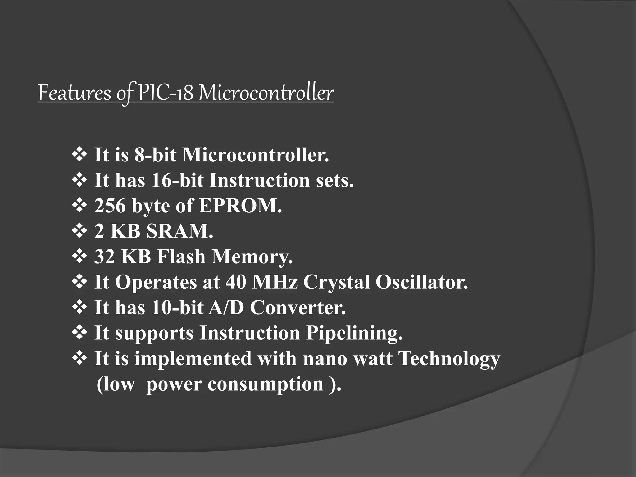
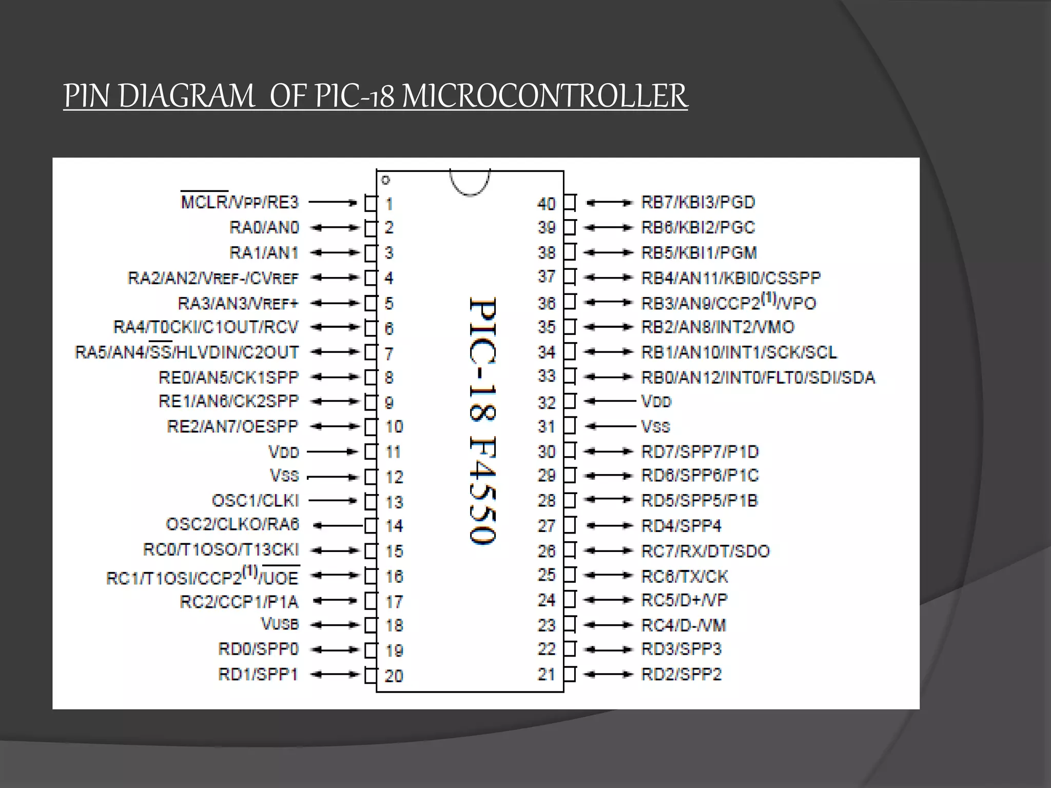
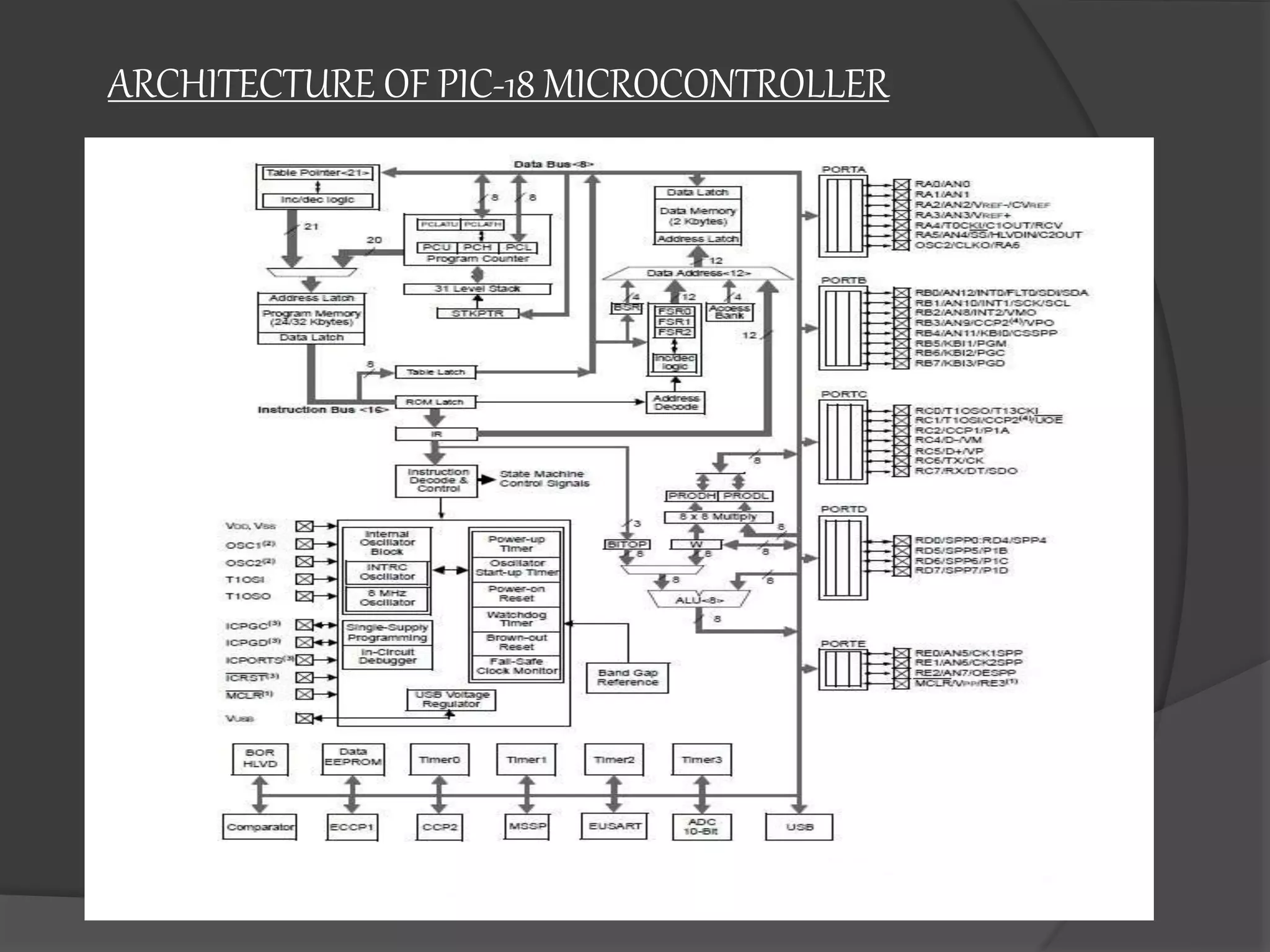
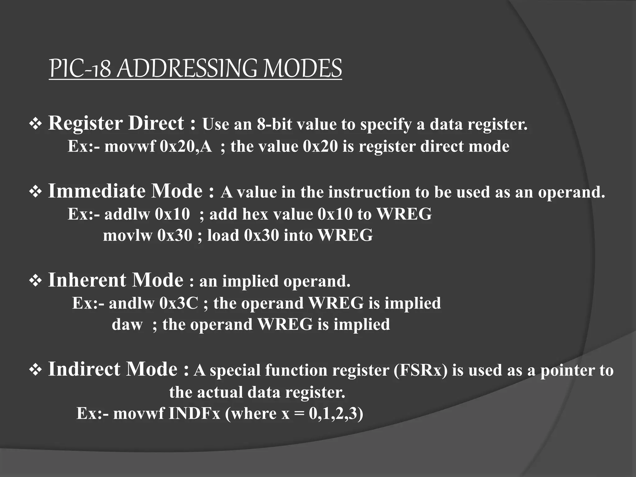
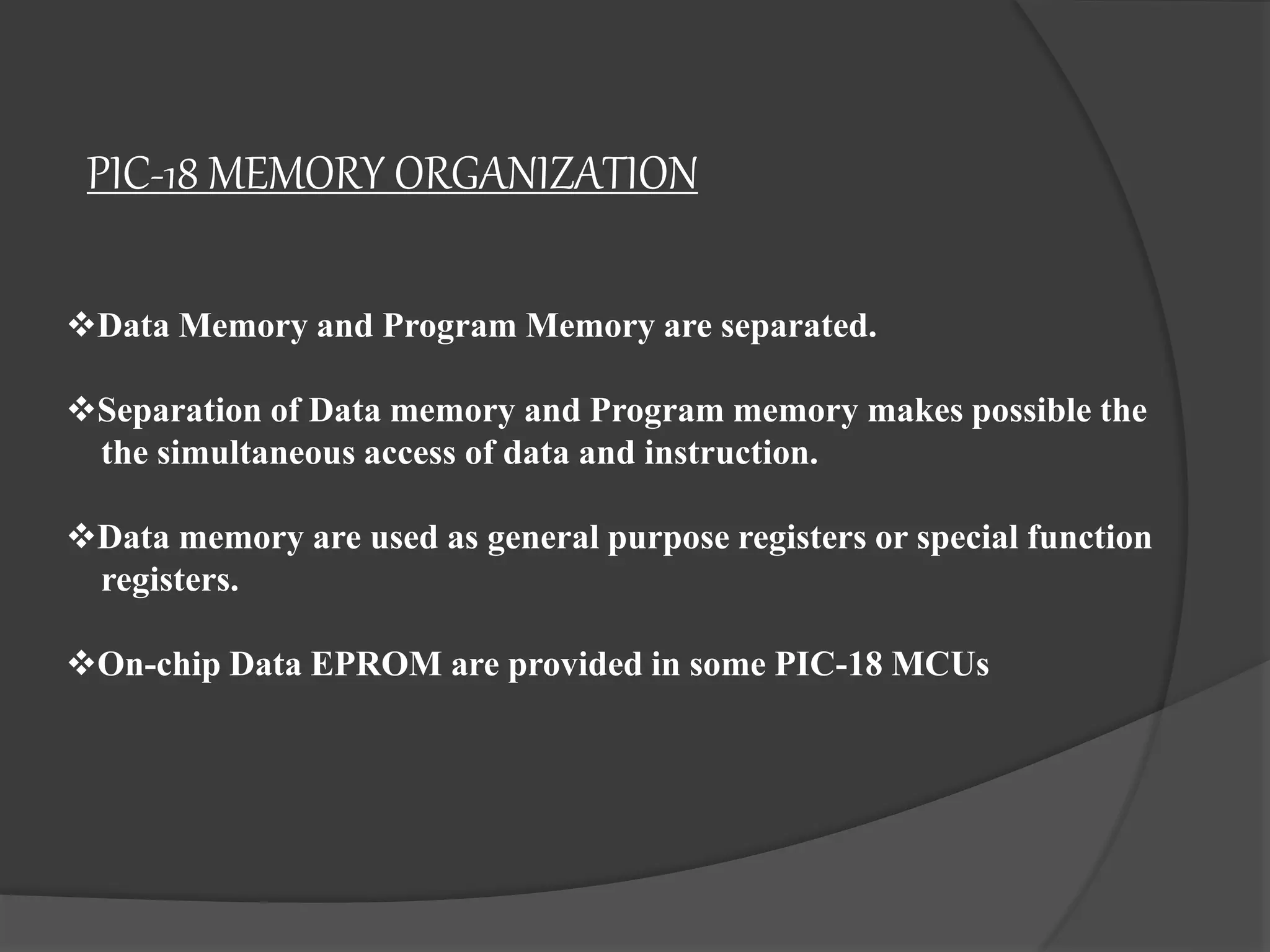
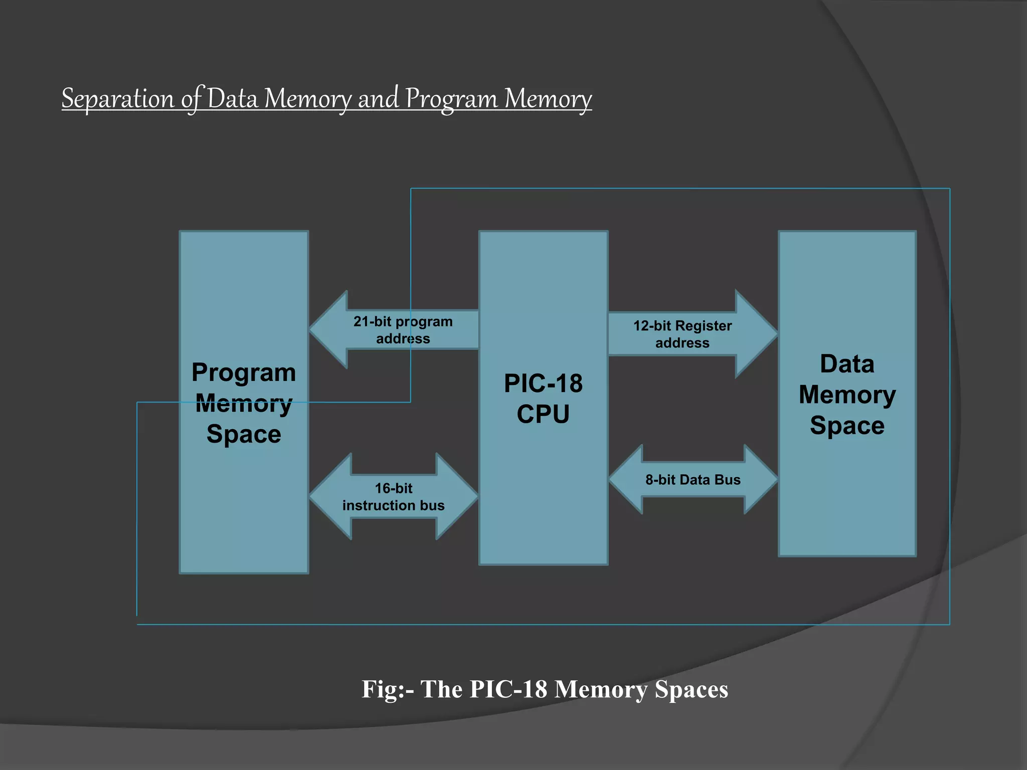
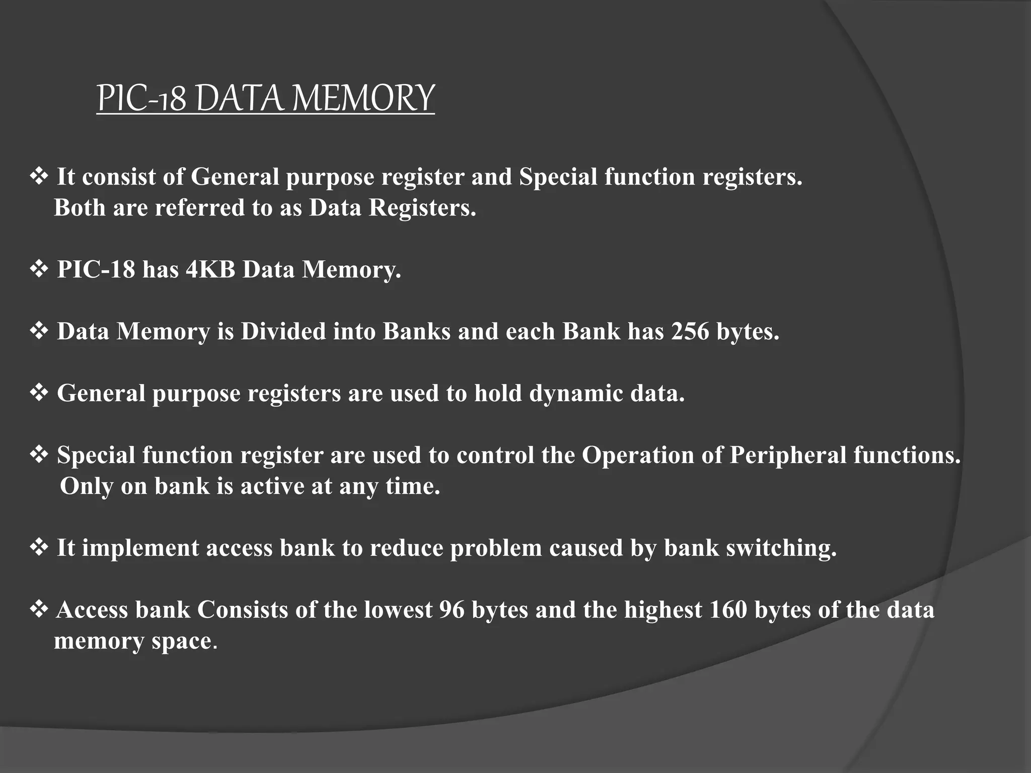
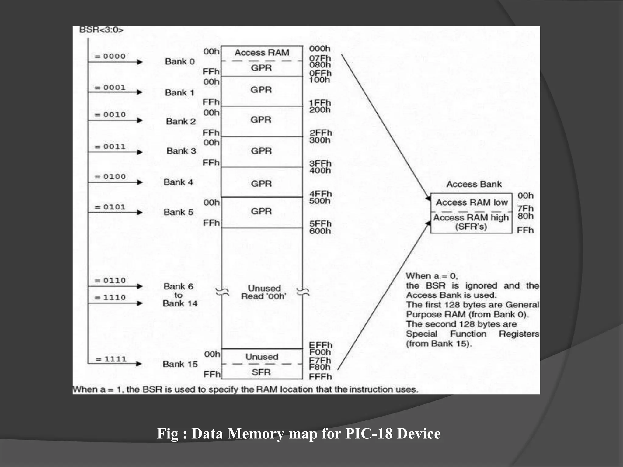
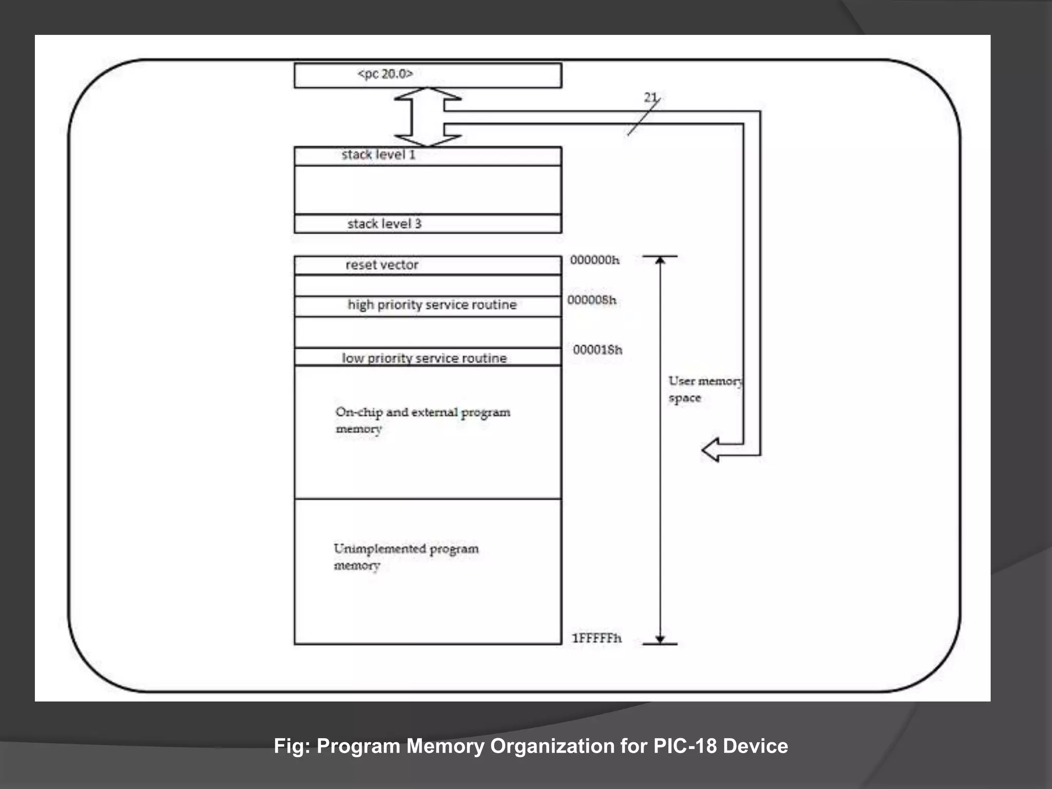
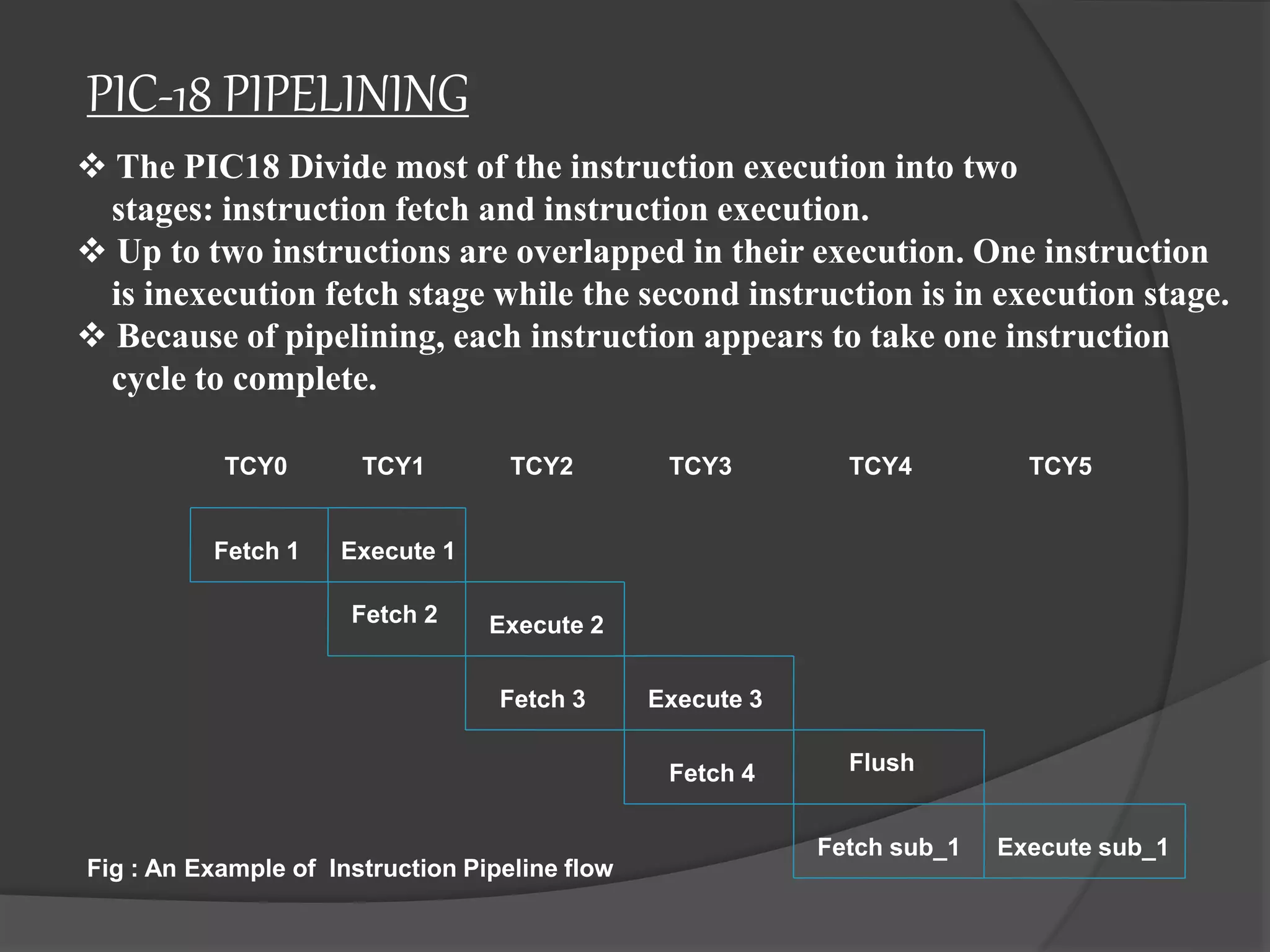
PIC-18 MICROCONTROLLER
PRESENTED BY:-
ASHISHRANJAN
What is Microcontroller ?
Microcontroller
8051 PIC ARM
TYPES OF MICROCONTROLLER
Features of PIC-18 Microcontroller
 It is 8-bit Microcontroller.
 It has 16-bit Instruction sets.
 256 byte of EPROM.
 2 KB SRAM.
 32 KB Flash Memory.
 It Operates at 40 MHz Crystal Oscillator.
 It has 10-bit A/D Converter.
 It supports Instruction Pipelining.
 It is implemented with nano watt Technology
(low power consumption ).
PIN DIAGRAM OF PIC-18 MICROCONTROLLER
ARCHITECTURE OF PIC-18 MICROCONTROLLER
PIC-18 ADDRESSING MODES
 Register Direct : Use an 8-bit value to specify a data register.
Ex:- movwf 0x20,A ; the value 0x20 is register direct mode
 Immediate Mode : A value in the instruction to be used as an operand.
Ex:- addlw 0x10 ; add hex value 0x10 to WREG
movlw 0x30 ; load 0x30 into WREG
 Inherent Mode : an implied operand.
Ex:- andlw 0x3C ; the operand WREG is implied
daw ; the operand WREG is implied
 Indirect Mode : A special function register (FSRx) is used as a pointer to
the actual data register.
Ex:- movwf INDFx (where x = 0,1,2,3)
PIC-18 MEMORY ORGANIZATION
Data Memory and Program Memory are separated.
Separation of Data memory and Program memory makes possible the
the simultaneous access of data and instruction.
Data memory are used as general purpose registers or special function
registers.
On-chip Data EPROM are provided in some PIC-18 MCUs
Separation of Data Memory and Program Memory
Program
Memory
Space
PIC-18
CPU
21-bit program
address
16-bit
instruction bus
Data
Memory
Space
12-bit Register
address
8-bit Data Bus
Fig:- The PIC-18 Memory Spaces
PIC-18 DATA MEMORY
 It consist of General purpose register and Special function registers.
Both are referred to as Data Registers.
 PIC-18 has 4KB Data Memory.
 Data Memory is Divided into Banks and each Bank has 256 bytes.
 General purpose registers are used to hold dynamic data.
 Special function register are used to control the Operation of Peripheral functions.
Only on bank is active at any time.
 It implement access bank to reduce problem caused by bank switching.
 Access bank Consists of the lowest 96 bytes and the highest 160 bytes of the data
memory space.
Fig : Data Memory map for PIC-18 Device
PROGRAM MEMORY ORGANIZATION
 The program counter (PC) is 21-bit long, which enables the user program to
access up to 2MB program memory.
 After Power On it starts to execute the instruction from address 0.
 The Location 0x08 is reserved for high-priority interrupt service routine.
 The Location 0x18 is reserved for low-priority interrupt service routine.
 Up to 128 KB of Program Memory is inside the MCU chip.
 Rest Part of the program memory is located outside of the MCU chip.
Fig: Program Memory Organization for PIC-18 Device
PIC-18 PIPELINING
 The PIC18 Divide most of the instruction execution into two
stages: instruction fetch and instruction execution.
 Up to two instructions are overlapped in their execution. One instruction
is inexecution fetch stage while the second instruction is in execution stage.
 Because of pipelining, each instruction appears to take one instruction
cycle to complete.
Fetch 2
Execute 1
Fetch 4
Fetch 3
Fetch 1
Execute 2
Execute 3
Execute sub_1Fetch sub_1
Flush
TCY0 TCY1 TCY2 TCY3 TCY4 TCY5
Fig : An Example of Instruction Pipeline flow
THANK YOU…..

PIC-18 Microcontroller

  • 1.
  • 2.
  • 3.
  • 4.
    Features of PIC-18Microcontroller  It is 8-bit Microcontroller.  It has 16-bit Instruction sets.  256 byte of EPROM.  2 KB SRAM.  32 KB Flash Memory.  It Operates at 40 MHz Crystal Oscillator.  It has 10-bit A/D Converter.  It supports Instruction Pipelining.  It is implemented with nano watt Technology (low power consumption ).
  • 5.
    PIN DIAGRAM OFPIC-18 MICROCONTROLLER
  • 6.
    ARCHITECTURE OF PIC-18MICROCONTROLLER
  • 7.
    PIC-18 ADDRESSING MODES Register Direct : Use an 8-bit value to specify a data register. Ex:- movwf 0x20,A ; the value 0x20 is register direct mode  Immediate Mode : A value in the instruction to be used as an operand. Ex:- addlw 0x10 ; add hex value 0x10 to WREG movlw 0x30 ; load 0x30 into WREG  Inherent Mode : an implied operand. Ex:- andlw 0x3C ; the operand WREG is implied daw ; the operand WREG is implied  Indirect Mode : A special function register (FSRx) is used as a pointer to the actual data register. Ex:- movwf INDFx (where x = 0,1,2,3)
  • 8.
    PIC-18 MEMORY ORGANIZATION DataMemory and Program Memory are separated. Separation of Data memory and Program memory makes possible the the simultaneous access of data and instruction. Data memory are used as general purpose registers or special function registers. On-chip Data EPROM are provided in some PIC-18 MCUs
  • 9.
    Separation of DataMemory and Program Memory Program Memory Space PIC-18 CPU 21-bit program address 16-bit instruction bus Data Memory Space 12-bit Register address 8-bit Data Bus Fig:- The PIC-18 Memory Spaces
  • 10.
    PIC-18 DATA MEMORY It consist of General purpose register and Special function registers. Both are referred to as Data Registers.  PIC-18 has 4KB Data Memory.  Data Memory is Divided into Banks and each Bank has 256 bytes.  General purpose registers are used to hold dynamic data.  Special function register are used to control the Operation of Peripheral functions. Only on bank is active at any time.  It implement access bank to reduce problem caused by bank switching.  Access bank Consists of the lowest 96 bytes and the highest 160 bytes of the data memory space.
  • 11.
    Fig : DataMemory map for PIC-18 Device
  • 12.
    PROGRAM MEMORY ORGANIZATION The program counter (PC) is 21-bit long, which enables the user program to access up to 2MB program memory.  After Power On it starts to execute the instruction from address 0.  The Location 0x08 is reserved for high-priority interrupt service routine.  The Location 0x18 is reserved for low-priority interrupt service routine.  Up to 128 KB of Program Memory is inside the MCU chip.  Rest Part of the program memory is located outside of the MCU chip.
  • 13.
    Fig: Program MemoryOrganization for PIC-18 Device
  • 14.
    PIC-18 PIPELINING  ThePIC18 Divide most of the instruction execution into two stages: instruction fetch and instruction execution.  Up to two instructions are overlapped in their execution. One instruction is inexecution fetch stage while the second instruction is in execution stage.  Because of pipelining, each instruction appears to take one instruction cycle to complete. Fetch 2 Execute 1 Fetch 4 Fetch 3 Fetch 1 Execute 2 Execute 3 Execute sub_1Fetch sub_1 Flush TCY0 TCY1 TCY2 TCY3 TCY4 TCY5 Fig : An Example of Instruction Pipeline flow
  • 15.