Debapriya Basu Roy
Departmentof Computer Science & Engineering
Indian Institute of Technology Kanpur
dbroy@cse.iitk.ac.in
dbroy24@gmail.com
ComputerOrganization:HardwareDescriptionLanguage
2.
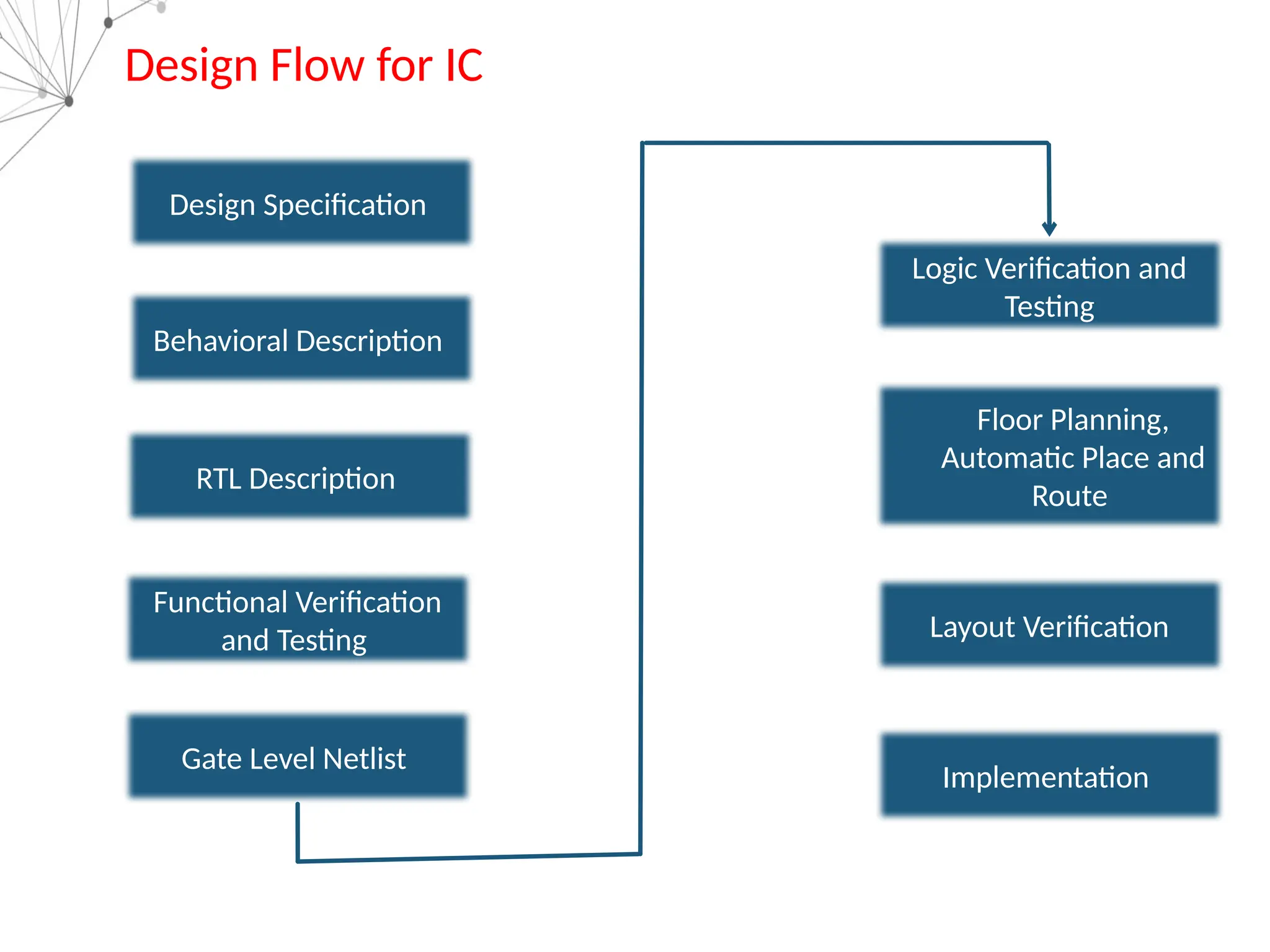
Design Specification
Behavioral Description
RTLDescription
Functional Verification
and Testing
Gate Level Netlist
Logic Verification and
Testing
Floor Planning,
Automatic Place and
Route
Layout Verification
Implementation
Design Flow for IC
3.
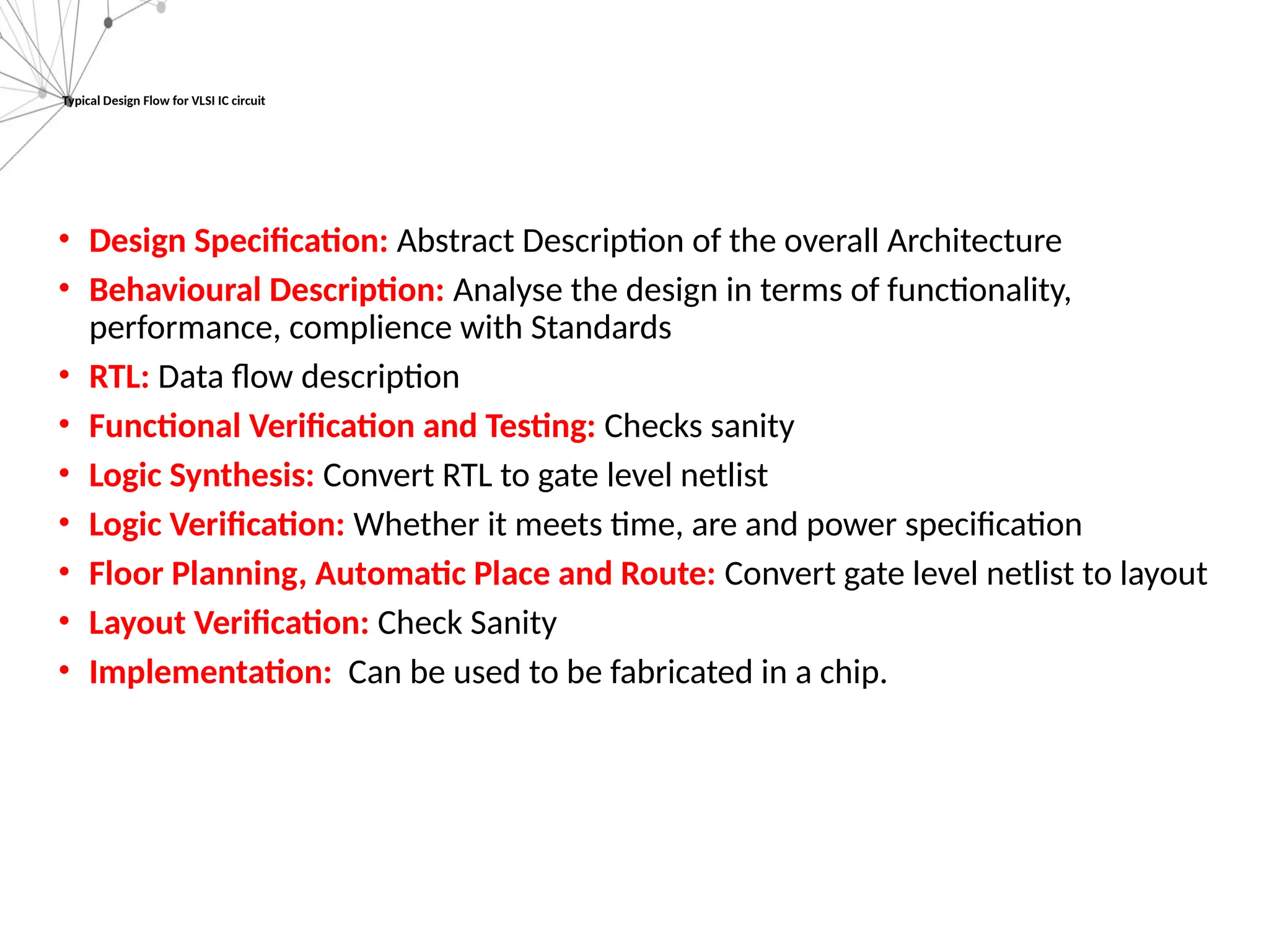
Typical Design Flowfor VLSI IC circuit
• Design Specification: Abstract Description of the overall Architecture
• Behavioural Description: Analyse the design in terms of functionality,
performance, complience with Standards
• RTL: Data flow description
• Functional Verification and Testing: Checks sanity
• Logic Synthesis: Convert RTL to gate level netlist
• Logic Verification: Whether it meets time, are and power specification
• Floor Planning, Automatic Place and Route: Convert gate level netlist to layout
• Layout Verification: Check Sanity
• Implementation: Can be used to be fabricated in a chip.
4.
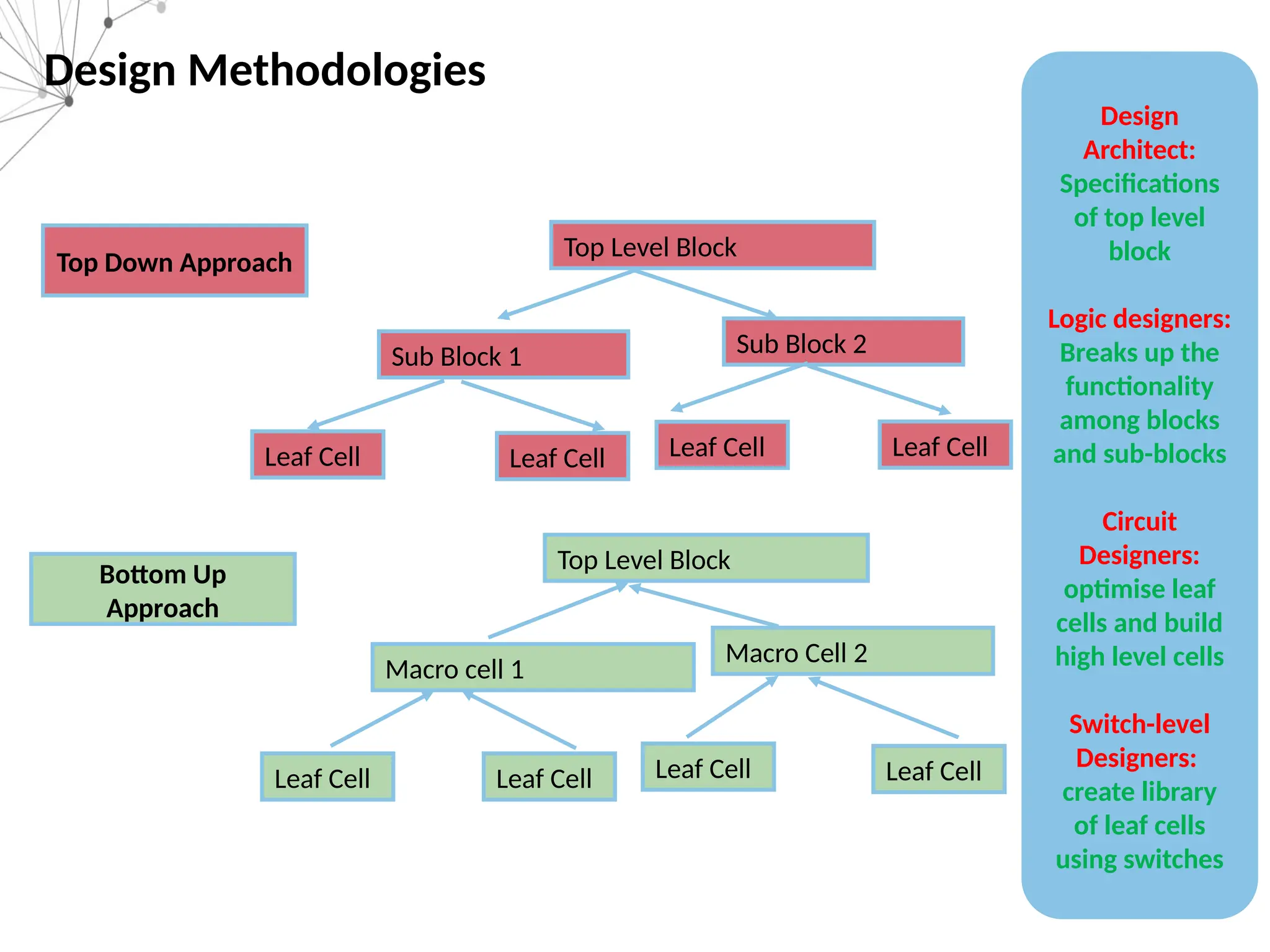
Design Methodologies
Top LevelBlock
Sub Block 1 Sub Block 2
Leaf Cell Leaf Cell Leaf Cell Leaf Cell
Top Down Approach
Top Level Block
Macro cell 1
Leaf Cell Leaf Cell Leaf Cell Leaf Cell
Macro Cell 2
Bottom Up
Approach
Design
Architect:
Specifications
of top level
block
Logic designers:
Breaks up the
functionality
among blocks
and sub-blocks
Circuit
Designers:
optimise leaf
cells and build
high level cells
Switch-level
Designers:
create library
of leaf cells
using switches
5.
What is Verilog
•Verilog is a Hardware Description Language, describing digital circuit using a programming language
• Difference with Standard programming language: Unlike C, Verilog has the capability of executing
statements both concurrently and sequentially.
• Verilog defines the circuit in a RTL (register transfer language)
• ASIC/ FPGA tool converts the circuit, defined by Verilog to gate level netlist (synthesis)
• Gate level netlist is placed and routed on the actual FPGA, incorporating the actual interconnect delay
• Other examples of HDL: VHDL (Very high speed integrated circuit HDL), Ada-like syntax, Bluespec
System Verilog
• Verilog was originated in 1983 at Gateway Design Automation; whereas VHDL was developed by
Defense Advanced Research Projects Agency (DAPRA) around 1987.
• Any circuit in Verilog can be defined by a block called module
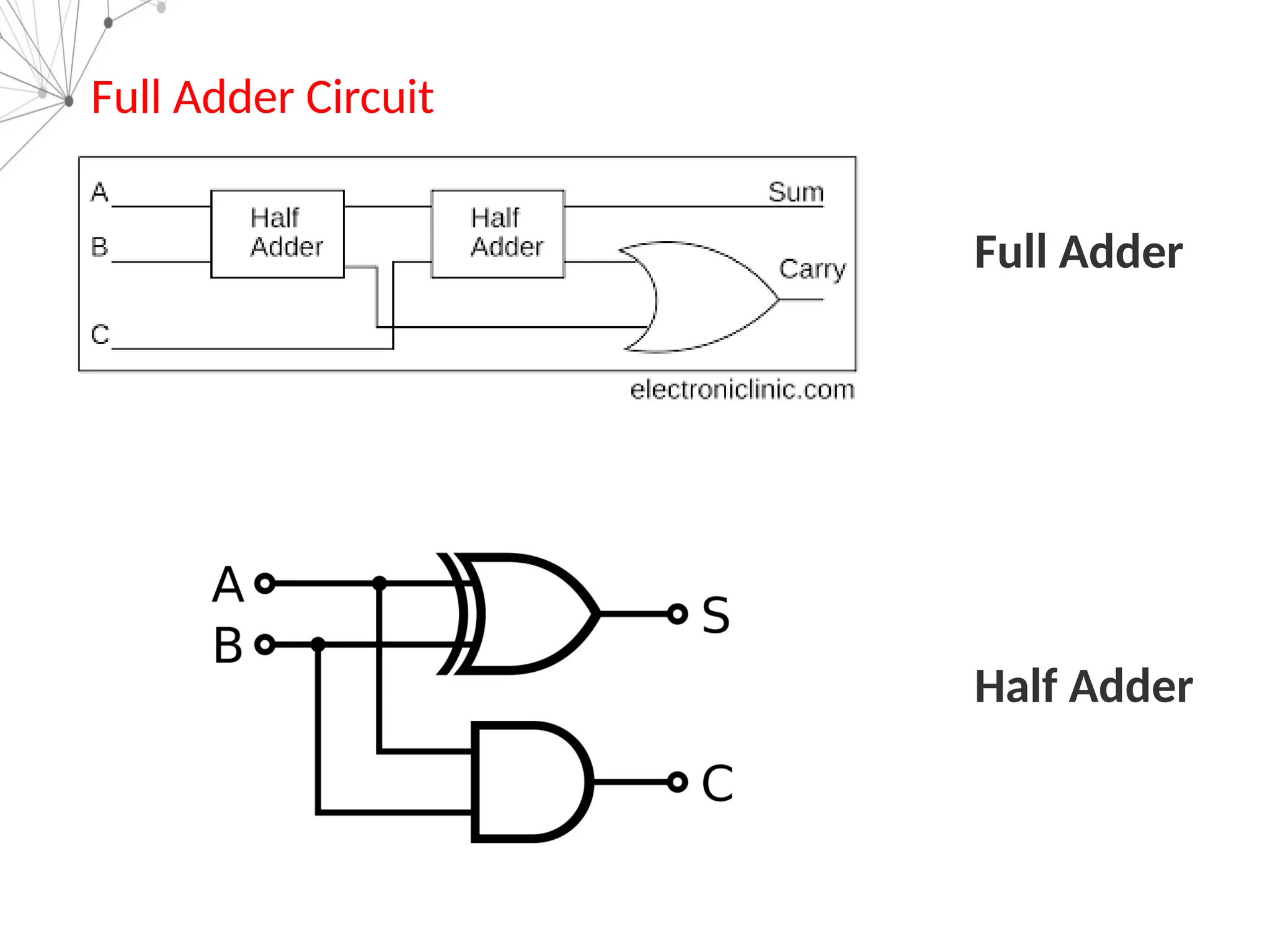
Full Adder
a
b
cin
s
cout
Full Adder Module
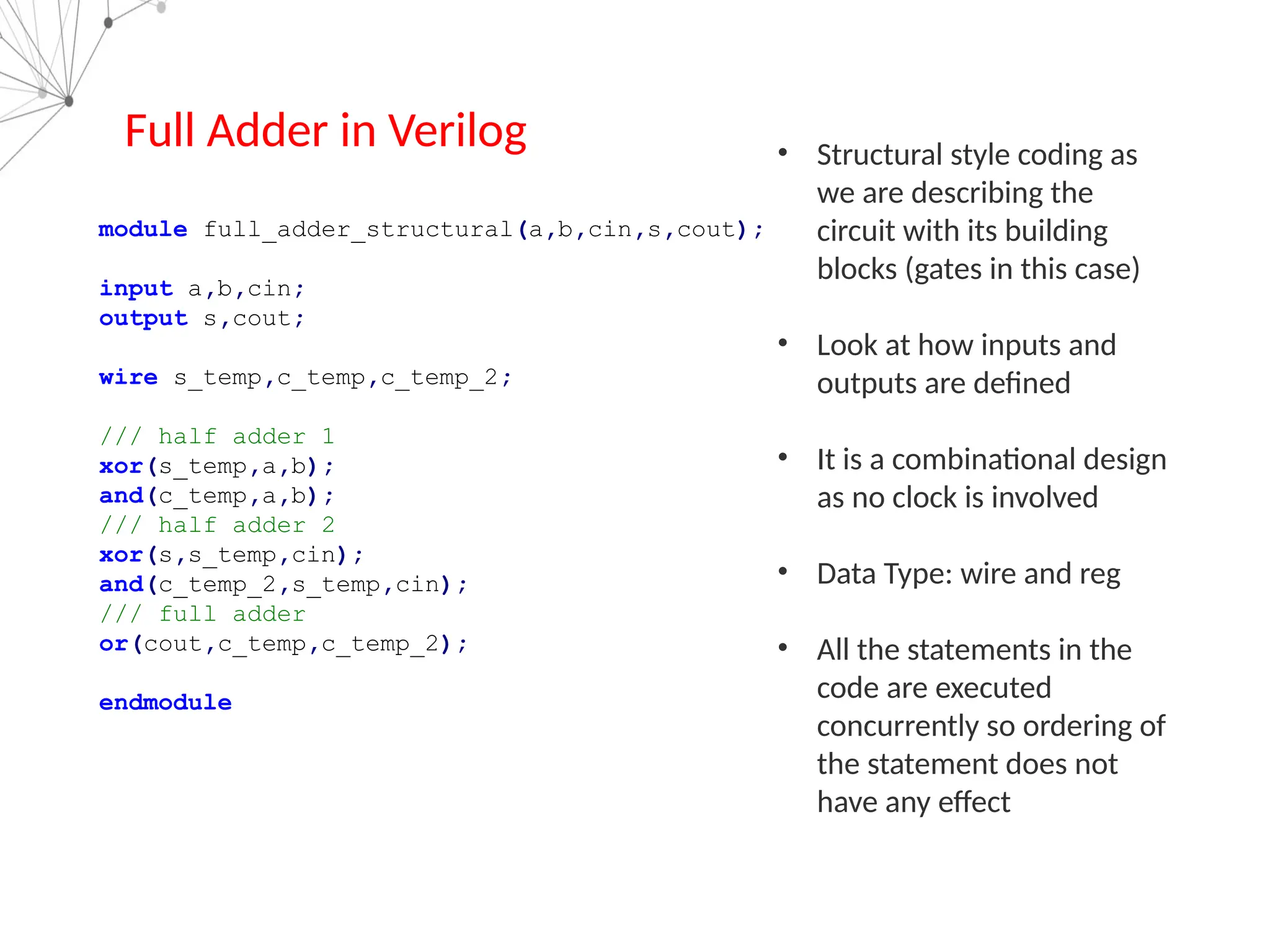
Full Adder inVerilog
module full_adder_structural(a,b,cin,s,cout);
input a,b,cin;
output s,cout;
wire s_temp,c_temp,c_temp_2;
/// half adder 1
xor(s_temp,a,b);
and(c_temp,a,b);
/// half adder 2
xor(s,s_temp,cin);
and(c_temp_2,s_temp,cin);
/// full adder
or(cout,c_temp,c_temp_2);
endmodule
• Structural style coding as
we are describing the
circuit with its building
blocks (gates in this case)
• Look at how inputs and
outputs are defined
• It is a combinational design
as no clock is involved
• Data Type: wire and reg
• All the statements in the
code are executed
concurrently so ordering of
the statement does not
have any effect
Ripple Carry Adderin Verilog
module RCA_adder_structural(a,b,sum,cout);
input [3:0] a,b;
output [3:0] sum;
output cout;
wire [3:0] c_temp;
full_adder_structural add1(a[1],b[1],c_temp[0],sum[1],c_temp[1]);
full_adder_structural add0(a[0],b[0],1'd0,sum[0],c_temp[0]);
full_adder_structural add2(a[2],b[2],c_temp[1],sum[2],c_temp[2]);
full_adder_structural add3(a[3],b[3],c_temp[2],sum[0],c_temp[3]);
assign c_out=c_temp[3];
endmodule
• How to declare a bit vector: wire [3:0] c_temp, input [3:0] a,b
• We have previously built full adder, and we are using that to build the ripple carry
adder. This process is called module instantiation
• Syntax : module_name instance_name module port_description
• assigning value to wire variable: assign c_out=c_temp[3];
10.
RCA with Parameterand Generate Block
module RCA_parameter_genvar(a,b,sum,cout);
parameter W=32;
input [W-1:0] a,b;
output [W-1:0] sum;
output cout;
wire [W:0] c_temp;
assign c_temp[0]=1'd0;
genvar i;
generate
for(i=0;i<W;i=i+1)
begin
full_adder_structural add0(a[i],b[i],c_temp[i],sum[i],c_temp[i+1]);
end
endgenerate
assign cout=c_temp[W];
endmodule
• Constant Declaration: 1’d0, 8’b11011101, 10’d1023, 8’hcf
• Look at the usage of parameter. Suppose we want to use this adder for 64 bit addition. We can
instantiate this code in the following way
RCA_parameter_genvar #(.W(64)) add(a,b,sum,cout);
• The for loop inside generate block allows multiple instantiations of the same module. The
generate blocks can also be used for many other purposes. We will revisit generate block again in
future
11.
2:1 Multiplexer: Ternaryoperator
A
B
Sel
out
module MUX_2_1(A,B,Sel,out);
parameter W=32;
input [W-1:0] A;
input [W-1:0] B;
input Sel;
output [W-1:0] out;
assign out=(Sel==0)?A:B;
endmodule
12.
4:1 Multiplexer: IfElse Block
module Mux_4_1(A,B,C,D,Sel,out);
parameter W=32;
input [W-1:0] A,B,C,D;
input [1:0] Sel;
output reg [W-1:0] out;
always@(*)
begin
if(Sel==2'd0)
begin
out<=A;
end
else if(Sel==2'd1)
begin
out<=B;
end
else if(Sel==2'd2)
begin
out<=C;
end
else
begin
out<=D;
end
end
endmodule
• Always Block: if else or case statements will always
execute either inside always block or generate block
• Variables which are updated inside the always block
are of datatype reg
• always@(a): This means that always block will get
executed when the signal a changes
• always@(a or b): This means that always block will
get executed when the signal a or signal b changes
• always@(*): This means that always block will get
executed whenever value of any signal changes
• Observe the statement: out<=c; This is an example
of non blocking assignment. We can also write
out=c; That will be a blocking assignment.
Difference between blocking and non blocking
assignment will become clear once we talk about
sequential circuit.
13.
8:1 Multiplexer: Casestatement
module Mux_8_1(A,B,C,D,E,F,G,H,Sel,out);
parameter W=32;
input [W-1:0] A,B,C,D,E,F,G,H;
input [2:0] Sel;
output reg [W-1:0] out;
always@(*)
begin
case(Sel)
3'd0:begin out<=A; end
3'd1:begin out<=B; end
3'd2:begin out<=C; end
3'd3:begin out<=D; end
3'd4:begin out<=E; end
3'd5:begin out<=F; end
3'd6:begin out<=G; end
default: begin out<=H; end
endcase
end
endmodule
• More elegant way of representing
Multiplexer
• Value of the output for each possible
state of case variable should be defined
14.
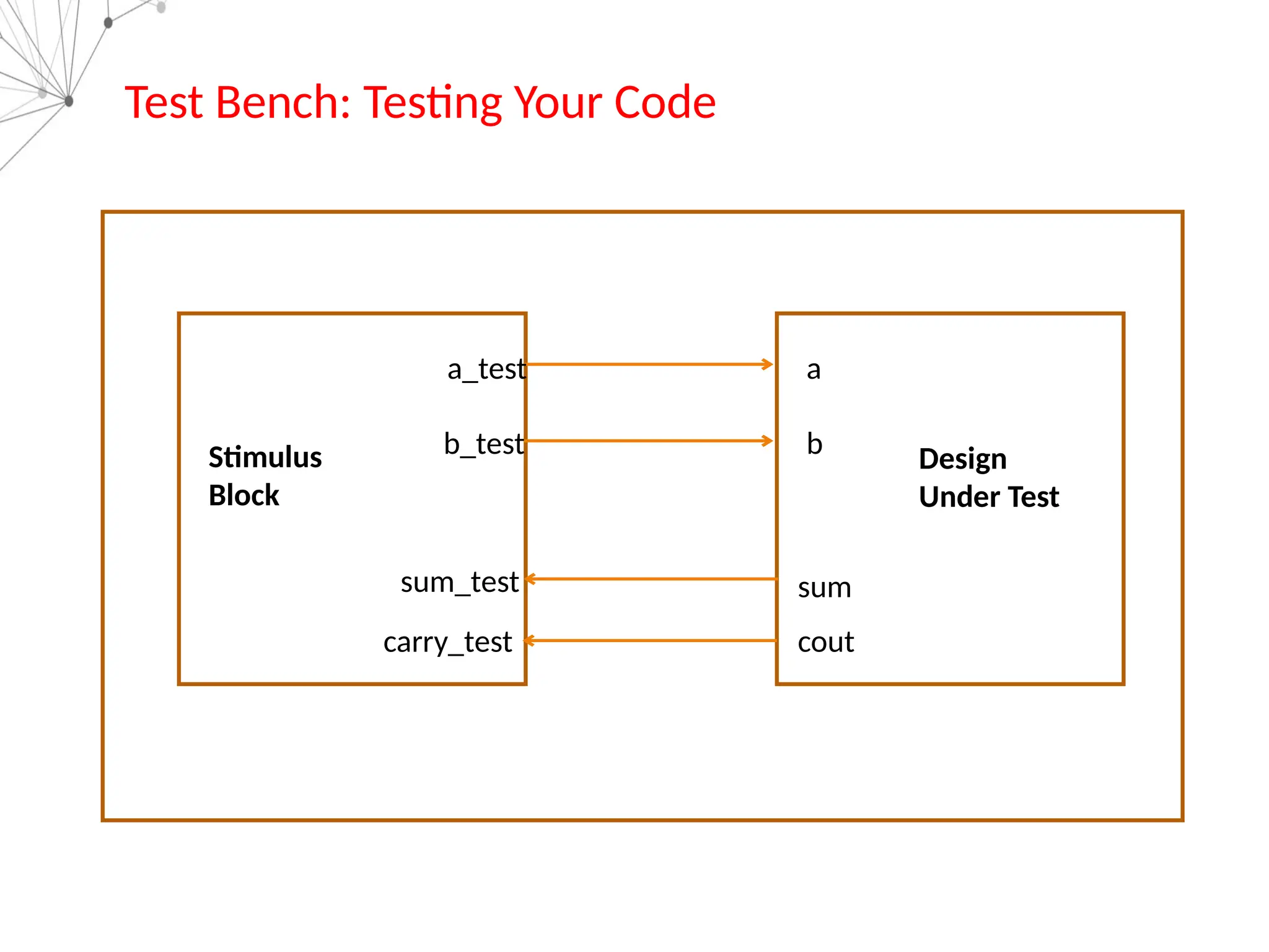
Test Bench: TestingYour Code
a_test
b_test
sum_test
carry_test
a
b
sum
cout
Stimulus
Block
Design
Under Test
15.
Test Bench: Example
moduletest_adder();
reg [3:0] a,b;
wire [3:0] sum;
wire cout;
initial begin
a<=4'd5; b<=4'd6;
#20
a<=4'd15; b<=4'd15;
#100
a<=4'd2; b<=4'd1;
end
RCA_adder_structural add(a,b,sum,cout);
endmodule
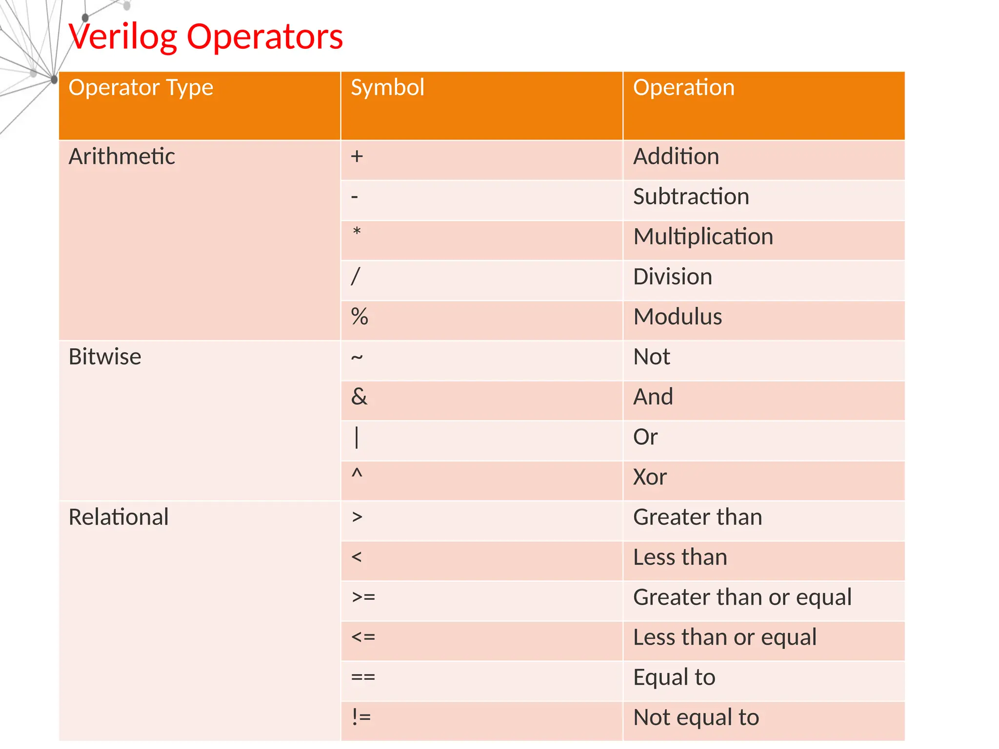
Verilog Operators
Operator TypeSymbol Operation
Arithmetic + Addition
- Subtraction
* Multiplication
/ Division
% Modulus
Bitwise ~ Not
& And
| Or
^ Xor
Relational > Greater than
< Less than
>= Greater than or equal
<= Less than or equal
== Equal to
!= Not equal to
19.
Verilog Operators
Operator TypeSymbol Operation
Logical ! Logical negation
&& Logical and
|| Logical or
Shift >> Right Shift
<< Left Shift
>>> Arithmetic right shift
<<< Arithmetic Left Shift
Concatenation {a,b} Join Variable a and b
Replication {n{b}} Replicate operand b n
times
Indexing/Slicing [MSB:LSB] Select the bits within
range MSB and LSB
module full_adder(a,b,cin,s,cout);
input a,b,cin;
outputs,cout;
assign s=a ^ b^ cin;
assign cout = (a & b) | (cin & (a ^ b));
endmodule
module RCA(a,b,sum,cout);
parameter W=32;
input [W-1:0] a,b;
output [W-1:0] sum;
output cout
assign {cout,sum}=a+b;
endmodule
Full Adder and RCA revisited
• Full Adder is
implemented using
bitwise operator
• RCA is implemented
using addition
operator
• Look at the usage of
concatenation
operator in RCA code
22.
Designing Sequential CircuitUsing Verilog
module D_flipflop(d,clk,rst,out);
input d,clk,rst;
output reg out;
always@(posedge clk)
begin
if(rst)
out<=0;
else
out<=d;
end
endmodule
module D_flipflop(d,clk,rst,out);
input d,clk,rst;
output reg out;
always@(posedge clk or posedge rst)
begin
if(rst)
out<=0;
else
out<=d;
end
endmodule
• Synchronous Reset D flip-flop vs Asynchronous reset D flip-flop
• Usage of non blocking assignment
• Let’s write a code for T flip-flop
23.
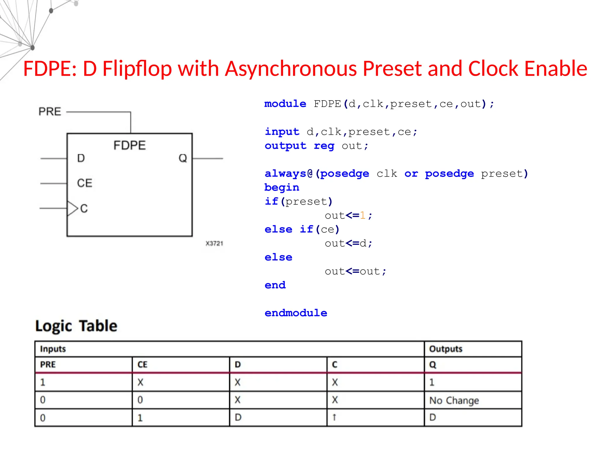
FDPE: D Flipflopwith Asynchronous Preset and Clock Enable
module FDPE(d,clk,preset,ce,out);
input d,clk,preset,ce;
output reg out;
always@(posedge clk or posedge preset)
begin
if(preset)
out<=1;
else if(ce)
out<=d;
else
out<=out;
end
endmodule
24.
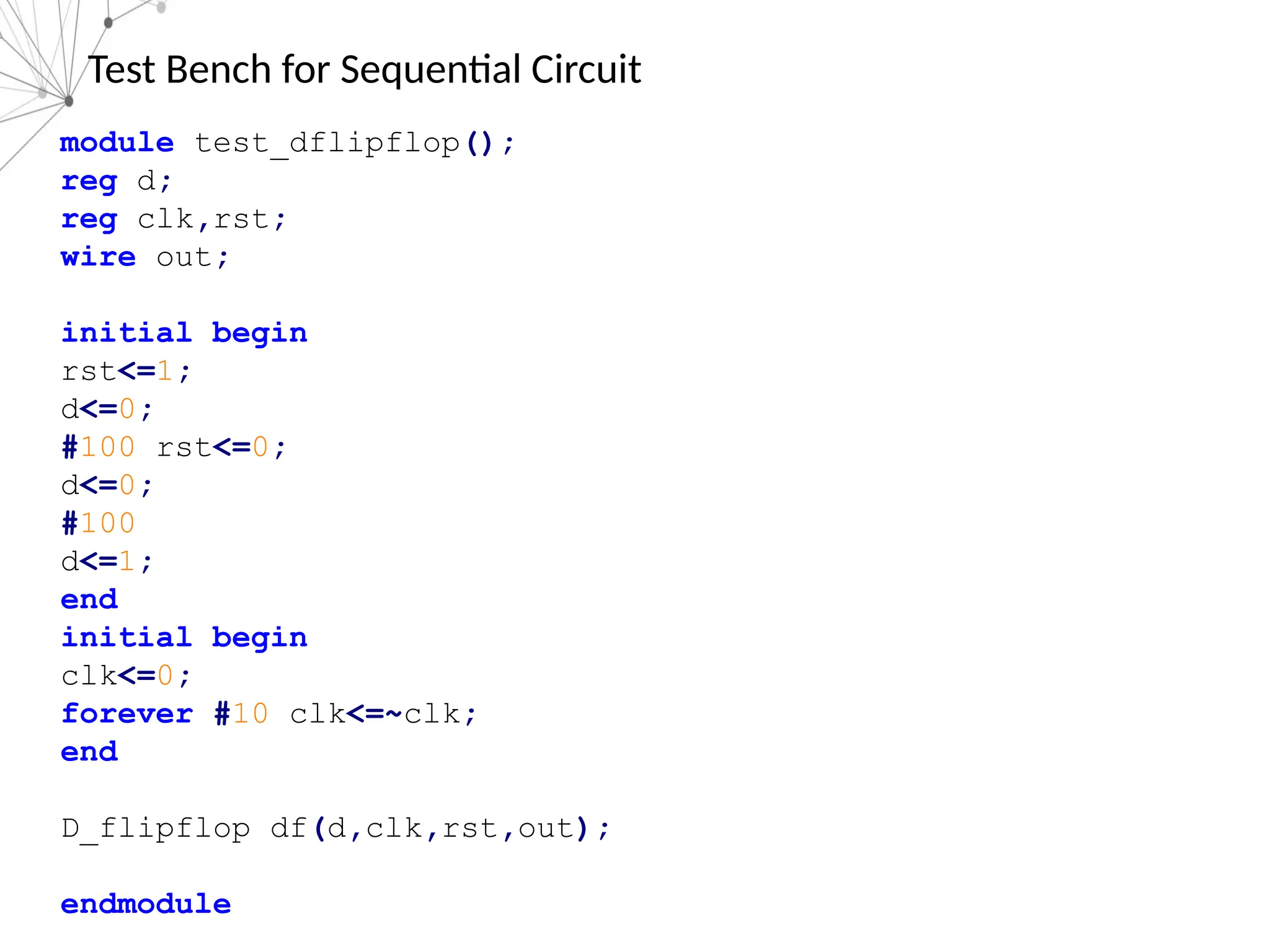
Test Bench forSequential Circuit
module test_dflipflop();
reg d;
reg clk,rst;
wire out;
initial begin
rst<=1;
d<=0;
#100 rst<=0;
d<=0;
#100
d<=1;
end
initial begin
clk<=0;
forever #10 clk<=~clk;
end
D_flipflop df(d,clk,rst,out);
endmodule
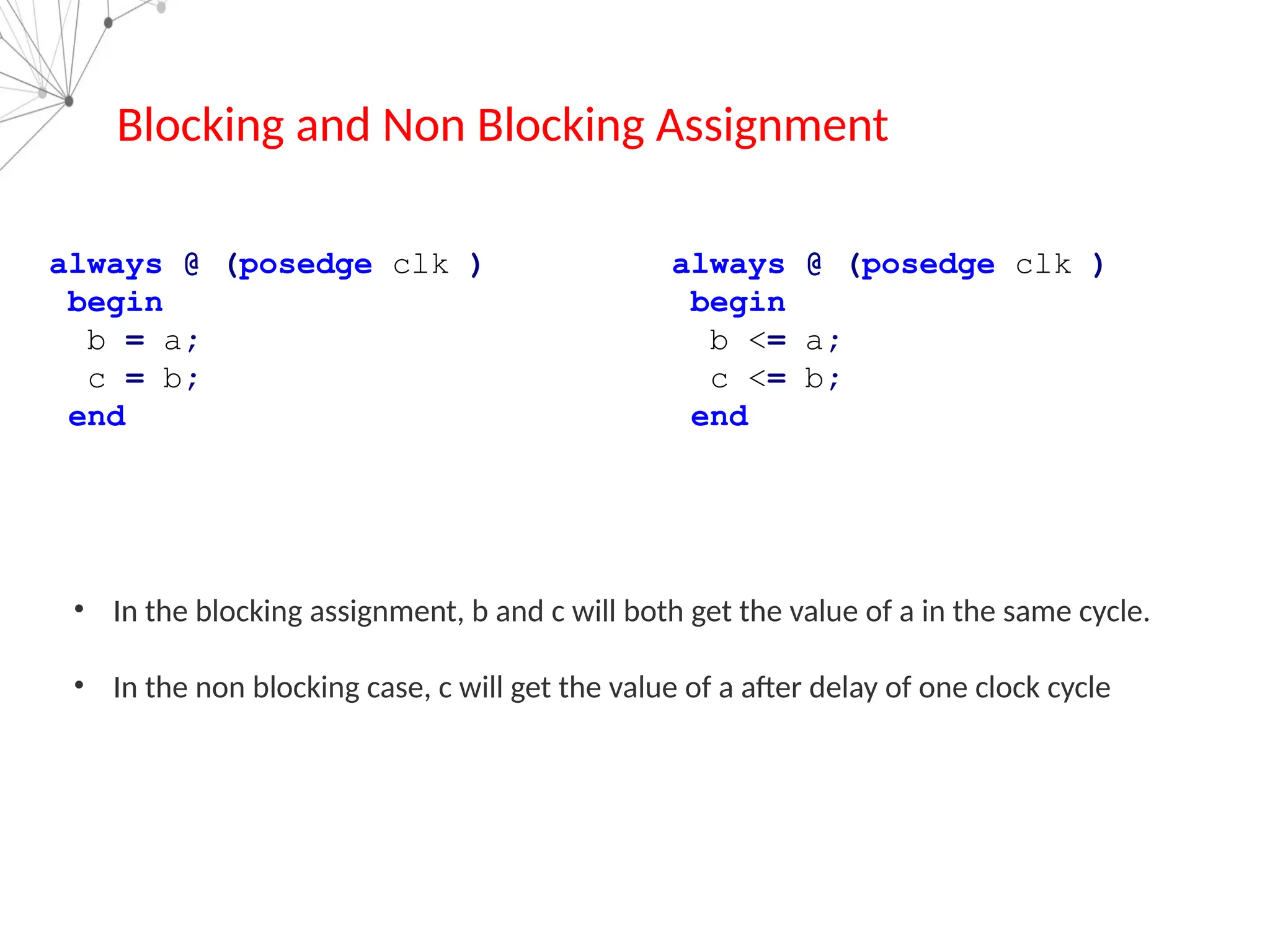
Blocking and NonBlocking Assignment
always @ (posedge clk )
begin
b = a;
c = b;
end
always @ (posedge clk )
begin
b <= a;
c <= b;
end
• In the blocking assignment, b and c will both get the value of a in the same cycle.
• In the non blocking case, c will get the value of a after delay of one clock cycle
27.
Write a codefor mod 10 counter
Reading Material: Chapter 2 and 3 from Samir
Palnitkar’s book


![Full
Adder
Full
Adder
Full
Adder
a[0]
b[0]
a[1]
b[1]
a[31]
b[31]
s[0]
s[1]
s[31]
. . .
Ripple Carry Adder
cout](https://image.slidesharecdn.com/lecture2verilogpart1preliminaries-250924165326-c793bf62/75/lecture_2_Verilog_Part-1_Preliminaries-pptx-8-2048.jpg)
![Ripple Carry Adder in Verilog
module RCA_adder_structural(a,b,sum,cout);
input [3:0] a,b;
output [3:0] sum;
output cout;
wire [3:0] c_temp;
full_adder_structural add1(a[1],b[1],c_temp[0],sum[1],c_temp[1]);
full_adder_structural add0(a[0],b[0],1'd0,sum[0],c_temp[0]);
full_adder_structural add2(a[2],b[2],c_temp[1],sum[2],c_temp[2]);
full_adder_structural add3(a[3],b[3],c_temp[2],sum[0],c_temp[3]);
assign c_out=c_temp[3];
endmodule
• How to declare a bit vector: wire [3:0] c_temp, input [3:0] a,b
• We have previously built full adder, and we are using that to build the ripple carry
adder. This process is called module instantiation
• Syntax : module_name instance_name module port_description
• assigning value to wire variable: assign c_out=c_temp[3];](https://image.slidesharecdn.com/lecture2verilogpart1preliminaries-250924165326-c793bf62/75/lecture_2_Verilog_Part-1_Preliminaries-pptx-9-2048.jpg)
![RCA with Parameter and Generate Block
module RCA_parameter_genvar(a,b,sum,cout);
parameter W=32;
input [W-1:0] a,b;
output [W-1:0] sum;
output cout;
wire [W:0] c_temp;
assign c_temp[0]=1'd0;
genvar i;
generate
for(i=0;i<W;i=i+1)
begin
full_adder_structural add0(a[i],b[i],c_temp[i],sum[i],c_temp[i+1]);
end
endgenerate
assign cout=c_temp[W];
endmodule
• Constant Declaration: 1’d0, 8’b11011101, 10’d1023, 8’hcf
• Look at the usage of parameter. Suppose we want to use this adder for 64 bit addition. We can
instantiate this code in the following way
RCA_parameter_genvar #(.W(64)) add(a,b,sum,cout);
• The for loop inside generate block allows multiple instantiations of the same module. The
generate blocks can also be used for many other purposes. We will revisit generate block again in
future](https://image.slidesharecdn.com/lecture2verilogpart1preliminaries-250924165326-c793bf62/75/lecture_2_Verilog_Part-1_Preliminaries-pptx-10-2048.jpg)
![2:1 Multiplexer: Ternary operator
A
B
Sel
out
module MUX_2_1(A,B,Sel,out);
parameter W=32;
input [W-1:0] A;
input [W-1:0] B;
input Sel;
output [W-1:0] out;
assign out=(Sel==0)?A:B;
endmodule](https://image.slidesharecdn.com/lecture2verilogpart1preliminaries-250924165326-c793bf62/75/lecture_2_Verilog_Part-1_Preliminaries-pptx-11-2048.jpg)
![4:1 Multiplexer: If Else Block
module Mux_4_1(A,B,C,D,Sel,out);
parameter W=32;
input [W-1:0] A,B,C,D;
input [1:0] Sel;
output reg [W-1:0] out;
always@(*)
begin
if(Sel==2'd0)
begin
out<=A;
end
else if(Sel==2'd1)
begin
out<=B;
end
else if(Sel==2'd2)
begin
out<=C;
end
else
begin
out<=D;
end
end
endmodule
• Always Block: if else or case statements will always
execute either inside always block or generate block
• Variables which are updated inside the always block
are of datatype reg
• always@(a): This means that always block will get
executed when the signal a changes
• always@(a or b): This means that always block will
get executed when the signal a or signal b changes
• always@(*): This means that always block will get
executed whenever value of any signal changes
• Observe the statement: out<=c; This is an example
of non blocking assignment. We can also write
out=c; That will be a blocking assignment.
Difference between blocking and non blocking
assignment will become clear once we talk about
sequential circuit.](https://image.slidesharecdn.com/lecture2verilogpart1preliminaries-250924165326-c793bf62/75/lecture_2_Verilog_Part-1_Preliminaries-pptx-12-2048.jpg)
![8:1 Multiplexer: Case statement
module Mux_8_1(A,B,C,D,E,F,G,H,Sel,out);
parameter W=32;
input [W-1:0] A,B,C,D,E,F,G,H;
input [2:0] Sel;
output reg [W-1:0] out;
always@(*)
begin
case(Sel)
3'd0:begin out<=A; end
3'd1:begin out<=B; end
3'd2:begin out<=C; end
3'd3:begin out<=D; end
3'd4:begin out<=E; end
3'd5:begin out<=F; end
3'd6:begin out<=G; end
default: begin out<=H; end
endcase
end
endmodule
• More elegant way of representing
Multiplexer
• Value of the output for each possible
state of case variable should be defined](https://image.slidesharecdn.com/lecture2verilogpart1preliminaries-250924165326-c793bf62/75/lecture_2_Verilog_Part-1_Preliminaries-pptx-13-2048.jpg)
![Test Bench: Example
module test_adder();
reg [3:0] a,b;
wire [3:0] sum;
wire cout;
initial begin
a<=4'd5; b<=4'd6;
#20
a<=4'd15; b<=4'd15;
#100
a<=4'd2; b<=4'd1;
end
RCA_adder_structural add(a,b,sum,cout);
endmodule](https://image.slidesharecdn.com/lecture2verilogpart1preliminaries-250924165326-c793bf62/75/lecture_2_Verilog_Part-1_Preliminaries-pptx-15-2048.jpg)
![module latch_code(a,b,sel,out);
input a,b;
input [2:0] sel;
output reg out;
always@(sel)
begin
if(sel==0)
out<=a;
else if(sel==1)
out<=b;
end
module latch_code(a,b,sel,out);
input a,b;
input [2:0] sel;
output reg out;
always@(sel)
begin
if(sel==0)
out<=a;
else if(sel==1)
out<=b;
else
out<=0;
end
Avoid Unintentional Latch Inference](https://image.slidesharecdn.com/lecture2verilogpart1preliminaries-250924165326-c793bf62/75/lecture_2_Verilog_Part-1_Preliminaries-pptx-16-2048.jpg)
![Verilog Operators
Operator Type Symbol Operation
Logical ! Logical negation
&& Logical and
|| Logical or
Shift >> Right Shift
<< Left Shift
>>> Arithmetic right shift
<<< Arithmetic Left Shift
Concatenation {a,b} Join Variable a and b
Replication {n{b}} Replicate operand b n
times
Indexing/Slicing [MSB:LSB] Select the bits within
range MSB and LSB](https://image.slidesharecdn.com/lecture2verilogpart1preliminaries-250924165326-c793bf62/75/lecture_2_Verilog_Part-1_Preliminaries-pptx-19-2048.jpg)
![wire [9:0] a;
wire [5:0] b;
wire [15:0] f;
wire [2:0] g;
wire [31:0] h;
assign a=10'h2ca;
assign b=6'h3f;
assign f={a,b};
assign g=b[4:2];
assign h={{2{a}},{2{b}}};
Predict the output of f, g, h](https://image.slidesharecdn.com/lecture2verilogpart1preliminaries-250924165326-c793bf62/75/lecture_2_Verilog_Part-1_Preliminaries-pptx-20-2048.jpg)
![module full_adder(a,b,cin,s,cout);
input a,b,cin;
output s,cout;
assign s=a ^ b^ cin;
assign cout = (a & b) | (cin & (a ^ b));
endmodule
module RCA(a,b,sum,cout);
parameter W=32;
input [W-1:0] a,b;
output [W-1:0] sum;
output cout
assign {cout,sum}=a+b;
endmodule
Full Adder and RCA revisited
• Full Adder is
implemented using
bitwise operator
• RCA is implemented
using addition
operator
• Look at the usage of
concatenation
operator in RCA code](https://image.slidesharecdn.com/lecture2verilogpart1preliminaries-250924165326-c793bf62/75/lecture_2_Verilog_Part-1_Preliminaries-pptx-21-2048.jpg)
![Counter Design using Verilog
module counter(clk,rst,count);
input clk,rst;
output reg [7:0] count;
always@(posedge clk)
begin
if([rst)
count<=0;
else
count<=count+1;
end
endmodule
module
counter(clk,rst,count,done);
input clk,rst;
output reg [7:0] count;
output done
always@(posedge clk)
begin
if([rst)
count<=0;
else if(count==8'd32)
count<=count;
else
count<=count+1;
end
assign done=(count==32)?1:0;
endmodule](https://image.slidesharecdn.com/lecture2verilogpart1preliminaries-250924165326-c793bf62/75/lecture_2_Verilog_Part-1_Preliminaries-pptx-25-2048.jpg)


![Full
Adder
Full
Adder
Full
Adder
a[0]
b[0]
a[1]
b[1]
a[31]
b[31]
s[0]
s[1]
s[31]
. . .
Ripple Carry Adder
cout](https://crownmelresort.com/image.slidesharecdn.com/lecture2verilogpart1preliminaries-250924165326-c793bf62/75/lecture_2_Verilog_Part-1_Preliminaries-pptx-8-2048.jpg)
![Ripple Carry Adder in Verilog
module RCA_adder_structural(a,b,sum,cout);
input [3:0] a,b;
output [3:0] sum;
output cout;
wire [3:0] c_temp;
full_adder_structural add1(a[1],b[1],c_temp[0],sum[1],c_temp[1]);
full_adder_structural add0(a[0],b[0],1'd0,sum[0],c_temp[0]);
full_adder_structural add2(a[2],b[2],c_temp[1],sum[2],c_temp[2]);
full_adder_structural add3(a[3],b[3],c_temp[2],sum[0],c_temp[3]);
assign c_out=c_temp[3];
endmodule
• How to declare a bit vector: wire [3:0] c_temp, input [3:0] a,b
• We have previously built full adder, and we are using that to build the ripple carry
adder. This process is called module instantiation
• Syntax : module_name instance_name module port_description
• assigning value to wire variable: assign c_out=c_temp[3];](https://crownmelresort.com/image.slidesharecdn.com/lecture2verilogpart1preliminaries-250924165326-c793bf62/75/lecture_2_Verilog_Part-1_Preliminaries-pptx-9-2048.jpg)
![RCA with Parameter and Generate Block
module RCA_parameter_genvar(a,b,sum,cout);
parameter W=32;
input [W-1:0] a,b;
output [W-1:0] sum;
output cout;
wire [W:0] c_temp;
assign c_temp[0]=1'd0;
genvar i;
generate
for(i=0;i<W;i=i+1)
begin
full_adder_structural add0(a[i],b[i],c_temp[i],sum[i],c_temp[i+1]);
end
endgenerate
assign cout=c_temp[W];
endmodule
• Constant Declaration: 1’d0, 8’b11011101, 10’d1023, 8’hcf
• Look at the usage of parameter. Suppose we want to use this adder for 64 bit addition. We can
instantiate this code in the following way
RCA_parameter_genvar #(.W(64)) add(a,b,sum,cout);
• The for loop inside generate block allows multiple instantiations of the same module. The
generate blocks can also be used for many other purposes. We will revisit generate block again in
future](https://crownmelresort.com/image.slidesharecdn.com/lecture2verilogpart1preliminaries-250924165326-c793bf62/75/lecture_2_Verilog_Part-1_Preliminaries-pptx-10-2048.jpg)
![2:1 Multiplexer: Ternary operator
A
B
Sel
out
module MUX_2_1(A,B,Sel,out);
parameter W=32;
input [W-1:0] A;
input [W-1:0] B;
input Sel;
output [W-1:0] out;
assign out=(Sel==0)?A:B;
endmodule](https://crownmelresort.com/image.slidesharecdn.com/lecture2verilogpart1preliminaries-250924165326-c793bf62/75/lecture_2_Verilog_Part-1_Preliminaries-pptx-11-2048.jpg)
![4:1 Multiplexer: If Else Block
module Mux_4_1(A,B,C,D,Sel,out);
parameter W=32;
input [W-1:0] A,B,C,D;
input [1:0] Sel;
output reg [W-1:0] out;
always@(*)
begin
if(Sel==2'd0)
begin
out<=A;
end
else if(Sel==2'd1)
begin
out<=B;
end
else if(Sel==2'd2)
begin
out<=C;
end
else
begin
out<=D;
end
end
endmodule
• Always Block: if else or case statements will always
execute either inside always block or generate block
• Variables which are updated inside the always block
are of datatype reg
• always@(a): This means that always block will get
executed when the signal a changes
• always@(a or b): This means that always block will
get executed when the signal a or signal b changes
• always@(*): This means that always block will get
executed whenever value of any signal changes
• Observe the statement: out<=c; This is an example
of non blocking assignment. We can also write
out=c; That will be a blocking assignment.
Difference between blocking and non blocking
assignment will become clear once we talk about
sequential circuit.](https://crownmelresort.com/image.slidesharecdn.com/lecture2verilogpart1preliminaries-250924165326-c793bf62/75/lecture_2_Verilog_Part-1_Preliminaries-pptx-12-2048.jpg)
![8:1 Multiplexer: Case statement
module Mux_8_1(A,B,C,D,E,F,G,H,Sel,out);
parameter W=32;
input [W-1:0] A,B,C,D,E,F,G,H;
input [2:0] Sel;
output reg [W-1:0] out;
always@(*)
begin
case(Sel)
3'd0:begin out<=A; end
3'd1:begin out<=B; end
3'd2:begin out<=C; end
3'd3:begin out<=D; end
3'd4:begin out<=E; end
3'd5:begin out<=F; end
3'd6:begin out<=G; end
default: begin out<=H; end
endcase
end
endmodule
• More elegant way of representing
Multiplexer
• Value of the output for each possible
state of case variable should be defined](https://crownmelresort.com/image.slidesharecdn.com/lecture2verilogpart1preliminaries-250924165326-c793bf62/75/lecture_2_Verilog_Part-1_Preliminaries-pptx-13-2048.jpg)

![Test Bench: Example
module test_adder();
reg [3:0] a,b;
wire [3:0] sum;
wire cout;
initial begin
a<=4'd5; b<=4'd6;
#20
a<=4'd15; b<=4'd15;
#100
a<=4'd2; b<=4'd1;
end
RCA_adder_structural add(a,b,sum,cout);
endmodule](https://crownmelresort.com/image.slidesharecdn.com/lecture2verilogpart1preliminaries-250924165326-c793bf62/75/lecture_2_Verilog_Part-1_Preliminaries-pptx-15-2048.jpg)
![module latch_code(a,b,sel,out);
input a,b;
input [2:0] sel;
output reg out;
always@(sel)
begin
if(sel==0)
out<=a;
else if(sel==1)
out<=b;
end
module latch_code(a,b,sel,out);
input a,b;
input [2:0] sel;
output reg out;
always@(sel)
begin
if(sel==0)
out<=a;
else if(sel==1)
out<=b;
else
out<=0;
end
Avoid Unintentional Latch Inference](https://crownmelresort.com/image.slidesharecdn.com/lecture2verilogpart1preliminaries-250924165326-c793bf62/75/lecture_2_Verilog_Part-1_Preliminaries-pptx-16-2048.jpg)


![Verilog Operators
Operator Type Symbol Operation
Logical ! Logical negation
&& Logical and
|| Logical or
Shift >> Right Shift
<< Left Shift
>>> Arithmetic right shift
<<< Arithmetic Left Shift
Concatenation {a,b} Join Variable a and b
Replication {n{b}} Replicate operand b n
times
Indexing/Slicing [MSB:LSB] Select the bits within
range MSB and LSB](https://crownmelresort.com/image.slidesharecdn.com/lecture2verilogpart1preliminaries-250924165326-c793bf62/75/lecture_2_Verilog_Part-1_Preliminaries-pptx-19-2048.jpg)
![wire [9:0] a;
wire [5:0] b;
wire [15:0] f;
wire [2:0] g;
wire [31:0] h;
assign a=10'h2ca;
assign b=6'h3f;
assign f={a,b};
assign g=b[4:2];
assign h={{2{a}},{2{b}}};
Predict the output of f, g, h](https://crownmelresort.com/image.slidesharecdn.com/lecture2verilogpart1preliminaries-250924165326-c793bf62/75/lecture_2_Verilog_Part-1_Preliminaries-pptx-20-2048.jpg)
![module full_adder(a,b,cin,s,cout);
input a,b,cin;
output s,cout;
assign s=a ^ b^ cin;
assign cout = (a & b) | (cin & (a ^ b));
endmodule
module RCA(a,b,sum,cout);
parameter W=32;
input [W-1:0] a,b;
output [W-1:0] sum;
output cout
assign {cout,sum}=a+b;
endmodule
Full Adder and RCA revisited
• Full Adder is
implemented using
bitwise operator
• RCA is implemented
using addition
operator
• Look at the usage of
concatenation
operator in RCA code](https://crownmelresort.com/image.slidesharecdn.com/lecture2verilogpart1preliminaries-250924165326-c793bf62/75/lecture_2_Verilog_Part-1_Preliminaries-pptx-21-2048.jpg)


![Counter Design using Verilog
module counter(clk,rst,count);
input clk,rst;
output reg [7:0] count;
always@(posedge clk)
begin
if([rst)
count<=0;
else
count<=count+1;
end
endmodule
module
counter(clk,rst,count,done);
input clk,rst;
output reg [7:0] count;
output done
always@(posedge clk)
begin
if([rst)
count<=0;
else if(count==8'd32)
count<=count;
else
count<=count+1;
end
assign done=(count==32)?1:0;
endmodule](https://crownmelresort.com/image.slidesharecdn.com/lecture2verilogpart1preliminaries-250924165326-c793bf62/75/lecture_2_Verilog_Part-1_Preliminaries-pptx-25-2048.jpg)