Download to read offline
![Sansar Chand Sankhyan Int. Journal of Engineering Research and Applications www.ijera.com
ISSN : 2248-9622, Vol. 4, Issue 7( Version 4), July 2014, pp.67-70
www.ijera.com 68|P a g e
control the bus, only oneis allowed to do so and the data is not corrupted.
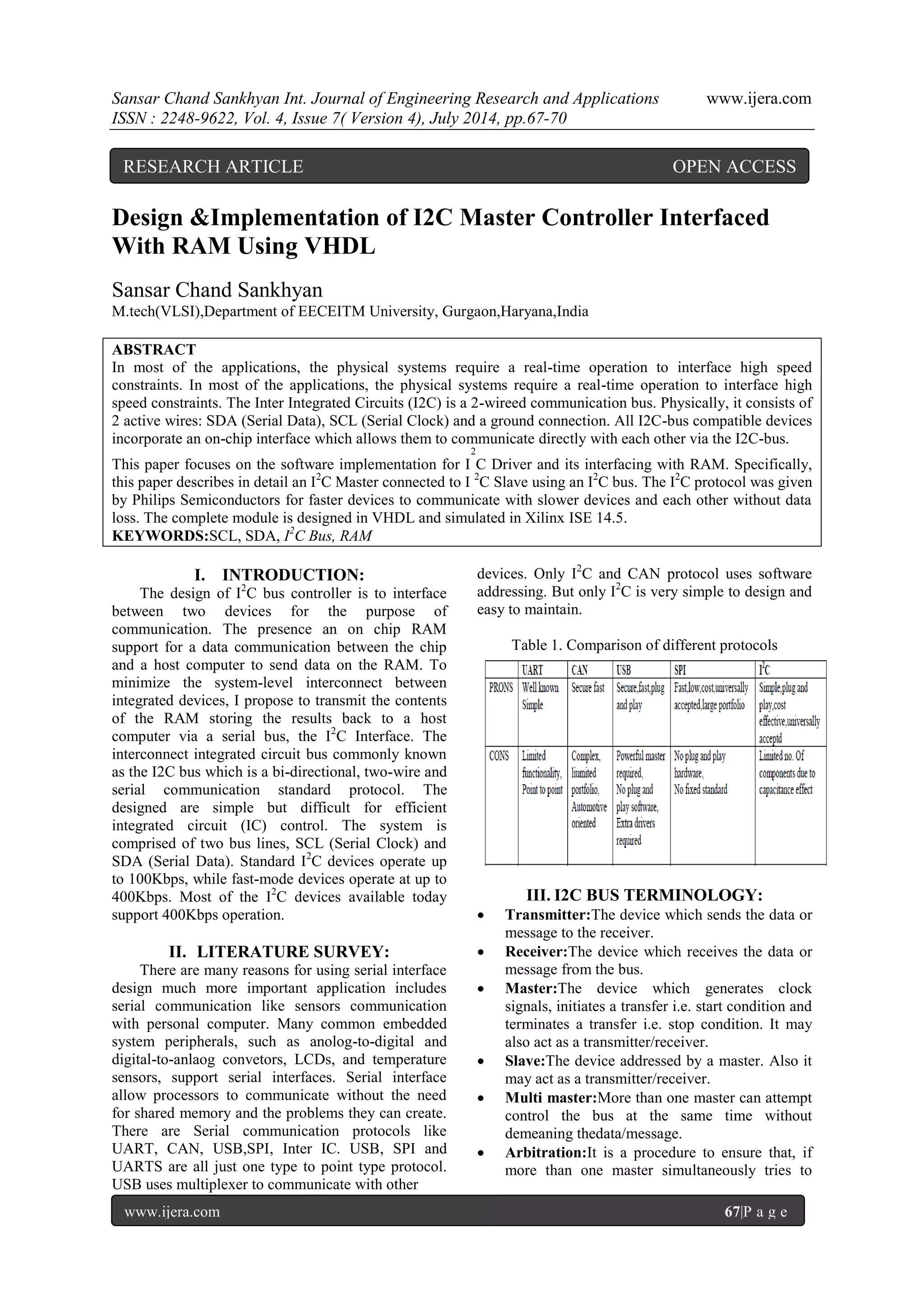
Synchronization:It is a procedure to synchronize the clock signals of two or more devices.
Figure 1. I2C bus configuration using masters and slaves
3.1 Master and Slave:
A master is the device which initiates a data transfer on the bus and generates theclock signals to permit that transfer. At that time, any device addressed is considered a slave.Both lines are connected to a positive supply via a pull-up resistor, and remain HIGH whenthe bus is not busy. Each device is recognized by a unique address—whether it is amicrocomputer, LCD driver, memory or keyboard interface—and can operate as either atransmitter or receiver, depending on the function of the device. A device generating amessage or data is a transmitter, and a device receiving the message or data is a receiver.Obviously, a passive function like an LCD driver could only be a receiver, while amicrocontroller or a memory can both transmit and receive data. When a data transfer takesplace on the bus, a device can either be a master or a slave. The device which initiates thetransfer, and generates the clock signals for this transfer, is the master. At that time anydevice addressed is considered a slave. It is important to note that a master could either be atransmitter or a receiver; a master microcontroller may send data to a RAM acting as atransmitter, and then interrogate the RAM for its contents acting as a receiver in both casesperforming as the master initiating the transfer. In the same manner, a slave could be both areceiver and a transmitter. The I2C is a multi master bus. It is possible to have, in one system; microcontroller may act as a master for one transfer, and then be theslave for another transfer, initiated by another processor on the network. The master/slave relationships on thebus are not permanent, and may change on each transfer.
3.2 Data Validity:
One data bit is transferred must remain stable during the HIGH period of the clock pulse in order to be valid. Changes in the data line at this time will be interpreted a eight bits long, is transferred serially with the most significant bit first, and is followed by an acknowledge bit. The clock pulse related to the acknowledge bit is generated by the master.
Figure2 Data validity condition
3.3 Byte format Data Transfer:
Every byte put on the SDA line must be 8 bits transmitted per transfer is unrestricted. Each byte has to be followed by an Acknowledge bit. Data is transferred with the Most Significant Bit (MSB) first. If a slave cannot receive or transmit another complete byte of data until it has performed other function, for example servicing an internal interrupt, it can hold the clock line SCL LOW to force the master into a wait state. Data transfer then continues when the slave is ready for another byte of data and releases clock line SCL
Figure 3 Data transfer on the I2C bus [7]
IV. I2C Protocol:
Normally, a standard communication protocol consists of four parts: 1) START signal generation 2) Slave address transfer 3) Data transfer 4) STOP signal generation
4.1 Transmitting a byte to a slave device:
After start condition has been sent, a byte can be transmitted to a slave by the master. This first byte after a startcondition will identify the slave on the bus (address) and will select the mode of operation. The meaning of all following bytes depends on the slave.](https://image.slidesharecdn.com/l0417046770-140909020617-phpapp01/75/Design-Implementation-of-I2C-Master-Controller-Interfaced-With-RAM-Using-VHDL-2-2048.jpg)
![Sansar Chand Sankhyan Int. Journal of Engineering Research and Applications www.ijera.com
ISSN : 2248-9622, Vol. 4, Issue 7( Version 4), July 2014, pp.67-70
www.ijera.com 69|P a g e
Figure 4 Transmission of a byte to a slave [8]
4.2 Receiving a byte from a slave device:
Once the slave has been addressed and the slave has acknowledged this, a byte can be received from the slave if the R/W bit in the address was set to READ (set to '1').
Figure 5 Reception of a byte from a slave [8]
4.3 Design steps:
The functional description of I2C master has to be described in the VHDL language. Thatis called design module / core.The test bench program has to be developed to test the design module. The test benchgives the input to the design module & verifies the outputs. The test bench has to bewritten in such way to check the design module in all possible conditions.
V. SYSTEM ARCHTECTURE:
Figure 6I2C and RAM interface system architecture In this paper we are considering master as I2C controller and slave as SDRAM.
5.1 Top-Level Signal Descriptions:
Figure 7 RTL schematic of designed I2C master controller Table-1 provides descriptions of the input/output signals of the I2C bus Master controller. The address bus is a 3-bit input pin to the I2C master controller. The data input to the master controller is 8-bit and data output from the master controller is also 8 bit. Serial data line (SDA) and Serial click line (SCL) both are out pins between the master controller and slave devices. RD and WR both are input pins to the master controller form microprocessor. Table 2. Signal Description of I2C Master Controller [7]
5.2 Process Algorithm:
The complete process of data transfer form master to slave and vice-versa is shown below in Figure 7in form of a algorithm .](https://image.slidesharecdn.com/l0417046770-140909020617-phpapp01/75/Design-Implementation-of-I2C-Master-Controller-Interfaced-With-RAM-Using-VHDL-3-2048.jpg)
![Sansar Chand Sankhyan Int. Journal of Engineering Research and Applications www.ijera.com
ISSN : 2248-9622, Vol. 4, Issue 7( Version 4), July 2014, pp.67-70
www.ijera.com 70|P a g e
Figure 8 Process flow of I2C controller [8]
5.3 Advantages OF I2C
1. Used for security sensitive applications like sensor connections, RFID, biometric devices, etc
2. Common communication standards between microcontrollers and sensors
3. Each device is recognised by its unique address and can operate as either a transmitter or receiver, depending upon thefunction of the device.
4. It Provides enhance security system
5. Compatible with FPGA
VI. SIMULATION RESULTS:
The VHDL code for I2C master controller is compiled in the Xilinx ISE 14.5 software tool. The test bench of this module is simulated and followings are the results.
Figure 9 Simulation result of write and read operation in I2C and RAM interface
VII. CONCLUSION:
The simulation results showed that all the designed functional blocks of the system design are giving desired results and the system itself also giving the desired results. The interfacing done between the I2C master controller and RAM slave is successfully designed and is giving desired results. The design module is designed using is done using VHDL. If the designer wants to design the module for any new technology than he only needs give the design to the logic synthesis tool as input and in result it will create the new gate level net list and the tool itself optimize the timing and area for new technology. References: [1] The I2C -Bus specifications version 2.1 January,2000http://www.semiconductors.philips.com/buses/i2c. [2] UM10204 I2C -bus specification and user manual Rev. 03 — 19 June 2007 [3] I2C bus Inter Integrated Circuits bus by Philips Semiconductors. [4] Embedded Platform Excalibur Altera, http://www.altera.com.
[5] PCF 8584, I2C bus controller datasheet,http://www.semiconductor.philips. com [6] www.latticesemi.com, I2C Master Controller reference design [7] Arvind Sahu, Ravi Shankar Mishra, Puran Gour, “Design and Interfacing of High speed model of FPGAS using I2C protocol”,Int.J.Com.Tech.Appl.vol2(3),531- 536 [8] Shoaib.Shah Sobhan, Sudipta. Das andIqbalur. Rahman, “Implementation of I2C using System Verilog and FPGA”,ICAEPE,2011. [9] Jayant Mankar et. al, “Review of I2C Protocol,” International Journal of Research in Advent Technology, vol. 2, issue 1, January 2014, pp.474-479. [10] A.K. Oudjida, M.L. Berrandjia, R. Tiar, A.Liacha, K. Tahraoui, with “FPGA Implementation of I2c & SPI Protocols: A Comparative Study” Electronics, Circuits, and Systems, 2009. ICECS.](https://image.slidesharecdn.com/l0417046770-140909020617-phpapp01/75/Design-Implementation-of-I2C-Master-Controller-Interfaced-With-RAM-Using-VHDL-4-2048.jpg)

![Sansar Chand Sankhyan Int. Journal of Engineering Research and Applications www.ijera.com
ISSN : 2248-9622, Vol. 4, Issue 7( Version 4), July 2014, pp.67-70
www.ijera.com 68|P a g e
control the bus, only oneis allowed to do so and the data is not corrupted.
Synchronization:It is a procedure to synchronize the clock signals of two or more devices.
Figure 1. I2C bus configuration using masters and slaves
3.1 Master and Slave:
A master is the device which initiates a data transfer on the bus and generates theclock signals to permit that transfer. At that time, any device addressed is considered a slave.Both lines are connected to a positive supply via a pull-up resistor, and remain HIGH whenthe bus is not busy. Each device is recognized by a unique address—whether it is amicrocomputer, LCD driver, memory or keyboard interface—and can operate as either atransmitter or receiver, depending on the function of the device. A device generating amessage or data is a transmitter, and a device receiving the message or data is a receiver.Obviously, a passive function like an LCD driver could only be a receiver, while amicrocontroller or a memory can both transmit and receive data. When a data transfer takesplace on the bus, a device can either be a master or a slave. The device which initiates thetransfer, and generates the clock signals for this transfer, is the master. At that time anydevice addressed is considered a slave. It is important to note that a master could either be atransmitter or a receiver; a master microcontroller may send data to a RAM acting as atransmitter, and then interrogate the RAM for its contents acting as a receiver in both casesperforming as the master initiating the transfer. In the same manner, a slave could be both areceiver and a transmitter. The I2C is a multi master bus. It is possible to have, in one system; microcontroller may act as a master for one transfer, and then be theslave for another transfer, initiated by another processor on the network. The master/slave relationships on thebus are not permanent, and may change on each transfer.
3.2 Data Validity:
One data bit is transferred must remain stable during the HIGH period of the clock pulse in order to be valid. Changes in the data line at this time will be interpreted a eight bits long, is transferred serially with the most significant bit first, and is followed by an acknowledge bit. The clock pulse related to the acknowledge bit is generated by the master.
Figure2 Data validity condition
3.3 Byte format Data Transfer:
Every byte put on the SDA line must be 8 bits transmitted per transfer is unrestricted. Each byte has to be followed by an Acknowledge bit. Data is transferred with the Most Significant Bit (MSB) first. If a slave cannot receive or transmit another complete byte of data until it has performed other function, for example servicing an internal interrupt, it can hold the clock line SCL LOW to force the master into a wait state. Data transfer then continues when the slave is ready for another byte of data and releases clock line SCL
Figure 3 Data transfer on the I2C bus [7]
IV. I2C Protocol:
Normally, a standard communication protocol consists of four parts: 1) START signal generation 2) Slave address transfer 3) Data transfer 4) STOP signal generation
4.1 Transmitting a byte to a slave device:
After start condition has been sent, a byte can be transmitted to a slave by the master. This first byte after a startcondition will identify the slave on the bus (address) and will select the mode of operation. The meaning of all following bytes depends on the slave.](https://crownmelresort.com/image.slidesharecdn.com/l0417046770-140909020617-phpapp01/75/Design-Implementation-of-I2C-Master-Controller-Interfaced-With-RAM-Using-VHDL-2-2048.jpg)
![Sansar Chand Sankhyan Int. Journal of Engineering Research and Applications www.ijera.com
ISSN : 2248-9622, Vol. 4, Issue 7( Version 4), July 2014, pp.67-70
www.ijera.com 69|P a g e
Figure 4 Transmission of a byte to a slave [8]
4.2 Receiving a byte from a slave device:
Once the slave has been addressed and the slave has acknowledged this, a byte can be received from the slave if the R/W bit in the address was set to READ (set to '1').
Figure 5 Reception of a byte from a slave [8]
4.3 Design steps:
The functional description of I2C master has to be described in the VHDL language. Thatis called design module / core.The test bench program has to be developed to test the design module. The test benchgives the input to the design module & verifies the outputs. The test bench has to bewritten in such way to check the design module in all possible conditions.
V. SYSTEM ARCHTECTURE:
Figure 6I2C and RAM interface system architecture In this paper we are considering master as I2C controller and slave as SDRAM.
5.1 Top-Level Signal Descriptions:
Figure 7 RTL schematic of designed I2C master controller Table-1 provides descriptions of the input/output signals of the I2C bus Master controller. The address bus is a 3-bit input pin to the I2C master controller. The data input to the master controller is 8-bit and data output from the master controller is also 8 bit. Serial data line (SDA) and Serial click line (SCL) both are out pins between the master controller and slave devices. RD and WR both are input pins to the master controller form microprocessor. Table 2. Signal Description of I2C Master Controller [7]
5.2 Process Algorithm:
The complete process of data transfer form master to slave and vice-versa is shown below in Figure 7in form of a algorithm .](https://crownmelresort.com/image.slidesharecdn.com/l0417046770-140909020617-phpapp01/75/Design-Implementation-of-I2C-Master-Controller-Interfaced-With-RAM-Using-VHDL-3-2048.jpg)
![Sansar Chand Sankhyan Int. Journal of Engineering Research and Applications www.ijera.com
ISSN : 2248-9622, Vol. 4, Issue 7( Version 4), July 2014, pp.67-70
www.ijera.com 70|P a g e
Figure 8 Process flow of I2C controller [8]
5.3 Advantages OF I2C
1. Used for security sensitive applications like sensor connections, RFID, biometric devices, etc
2. Common communication standards between microcontrollers and sensors
3. Each device is recognised by its unique address and can operate as either a transmitter or receiver, depending upon thefunction of the device.
4. It Provides enhance security system
5. Compatible with FPGA
VI. SIMULATION RESULTS:
The VHDL code for I2C master controller is compiled in the Xilinx ISE 14.5 software tool. The test bench of this module is simulated and followings are the results.
Figure 9 Simulation result of write and read operation in I2C and RAM interface
VII. CONCLUSION:
The simulation results showed that all the designed functional blocks of the system design are giving desired results and the system itself also giving the desired results. The interfacing done between the I2C master controller and RAM slave is successfully designed and is giving desired results. The design module is designed using is done using VHDL. If the designer wants to design the module for any new technology than he only needs give the design to the logic synthesis tool as input and in result it will create the new gate level net list and the tool itself optimize the timing and area for new technology. References: [1] The I2C -Bus specifications version 2.1 January,2000http://www.semiconductors.philips.com/buses/i2c. [2] UM10204 I2C -bus specification and user manual Rev. 03 — 19 June 2007 [3] I2C bus Inter Integrated Circuits bus by Philips Semiconductors. [4] Embedded Platform Excalibur Altera, http://www.altera.com.
[5] PCF 8584, I2C bus controller datasheet,http://www.semiconductor.philips. com [6] www.latticesemi.com, I2C Master Controller reference design [7] Arvind Sahu, Ravi Shankar Mishra, Puran Gour, “Design and Interfacing of High speed model of FPGAS using I2C protocol”,Int.J.Com.Tech.Appl.vol2(3),531- 536 [8] Shoaib.Shah Sobhan, Sudipta. Das andIqbalur. Rahman, “Implementation of I2C using System Verilog and FPGA”,ICAEPE,2011. [9] Jayant Mankar et. al, “Review of I2C Protocol,” International Journal of Research in Advent Technology, vol. 2, issue 1, January 2014, pp.474-479. [10] A.K. Oudjida, M.L. Berrandjia, R. Tiar, A.Liacha, K. Tahraoui, with “FPGA Implementation of I2c & SPI Protocols: A Comparative Study” Electronics, Circuits, and Systems, 2009. ICECS.](https://crownmelresort.com/image.slidesharecdn.com/l0417046770-140909020617-phpapp01/75/Design-Implementation-of-I2C-Master-Controller-Interfaced-With-RAM-Using-VHDL-4-2048.jpg)

This document discusses the design and implementation of an I2C master controller interfaced with RAM using VHDL, aimed at facilitating real-time communication between devices in embedded systems. It covers the I2C protocol, including terminology and data transfer protocols, detailing the operation of master and slave devices. The results demonstrate successful communication between the I2C master controller and RAM, with the design easily adaptable for future technologies.