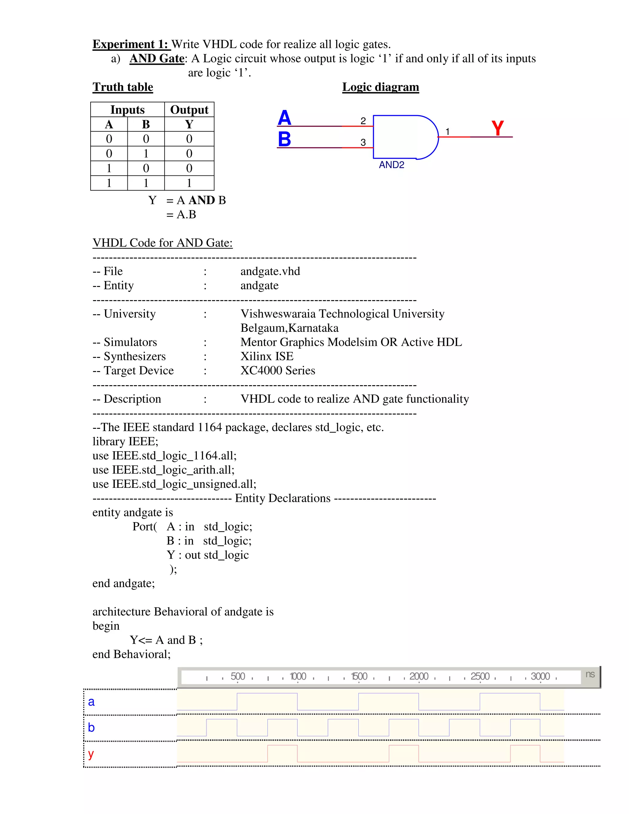
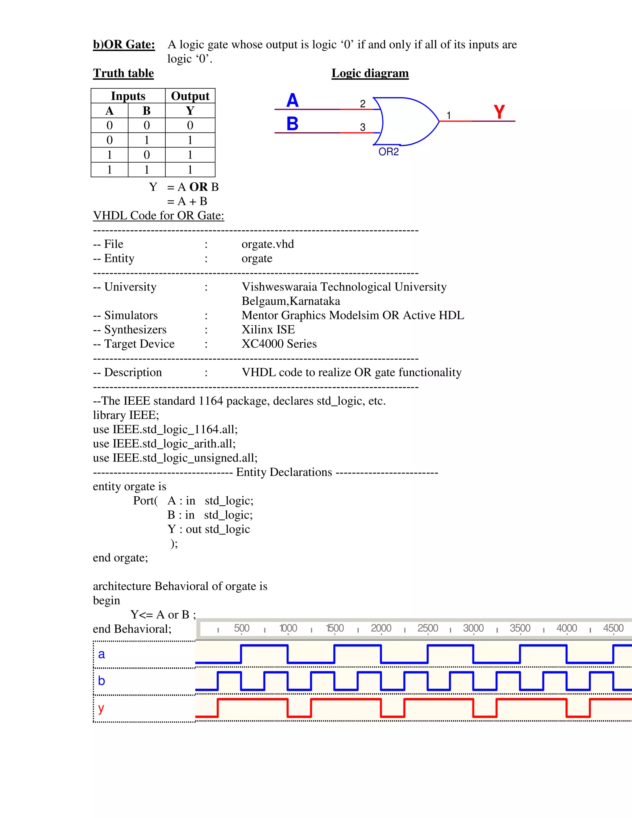
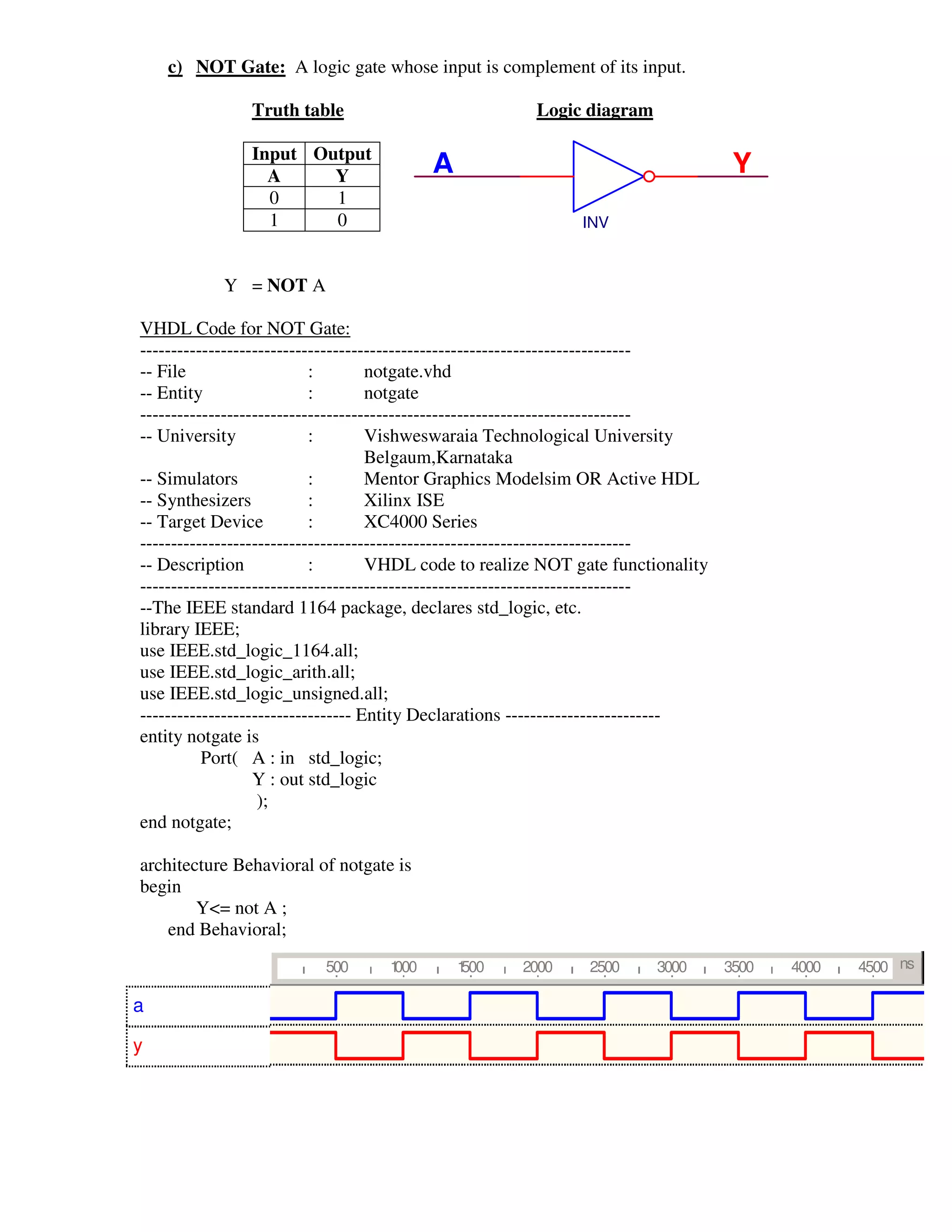
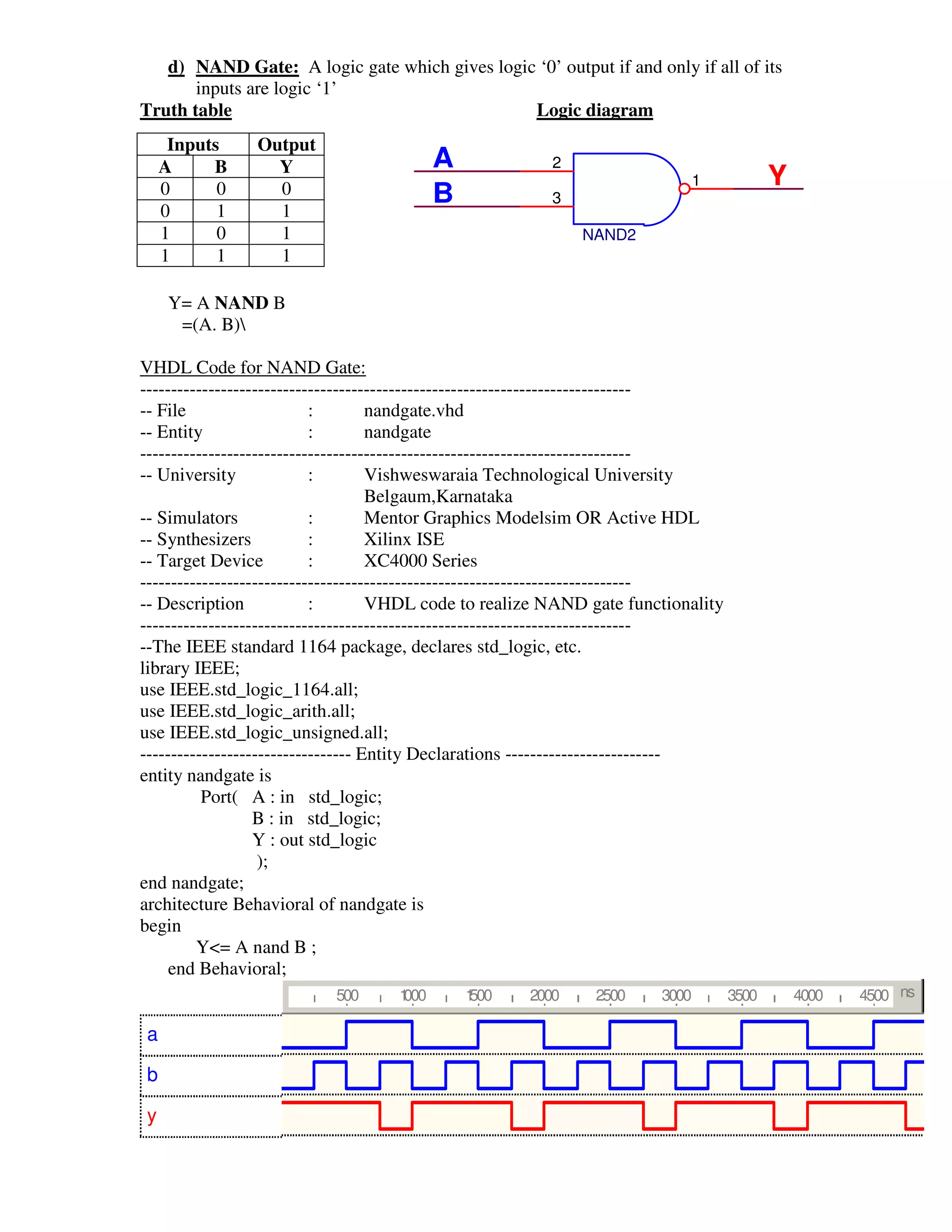
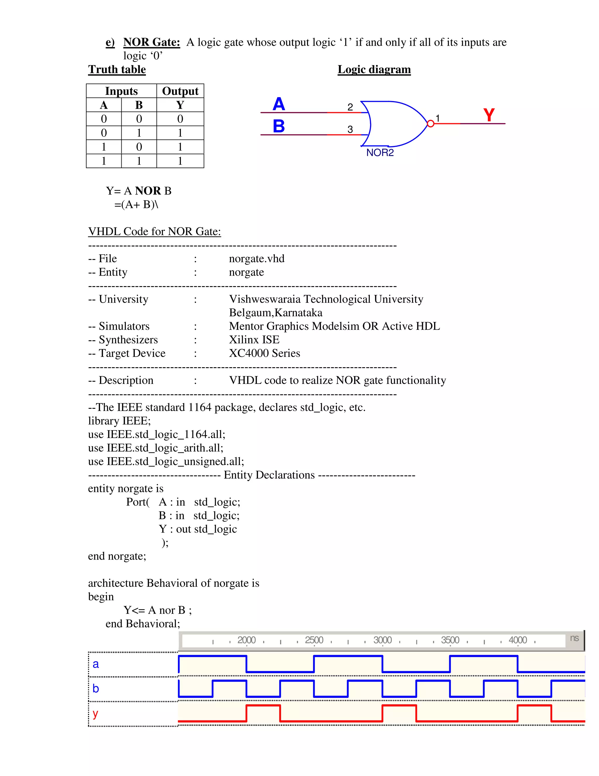
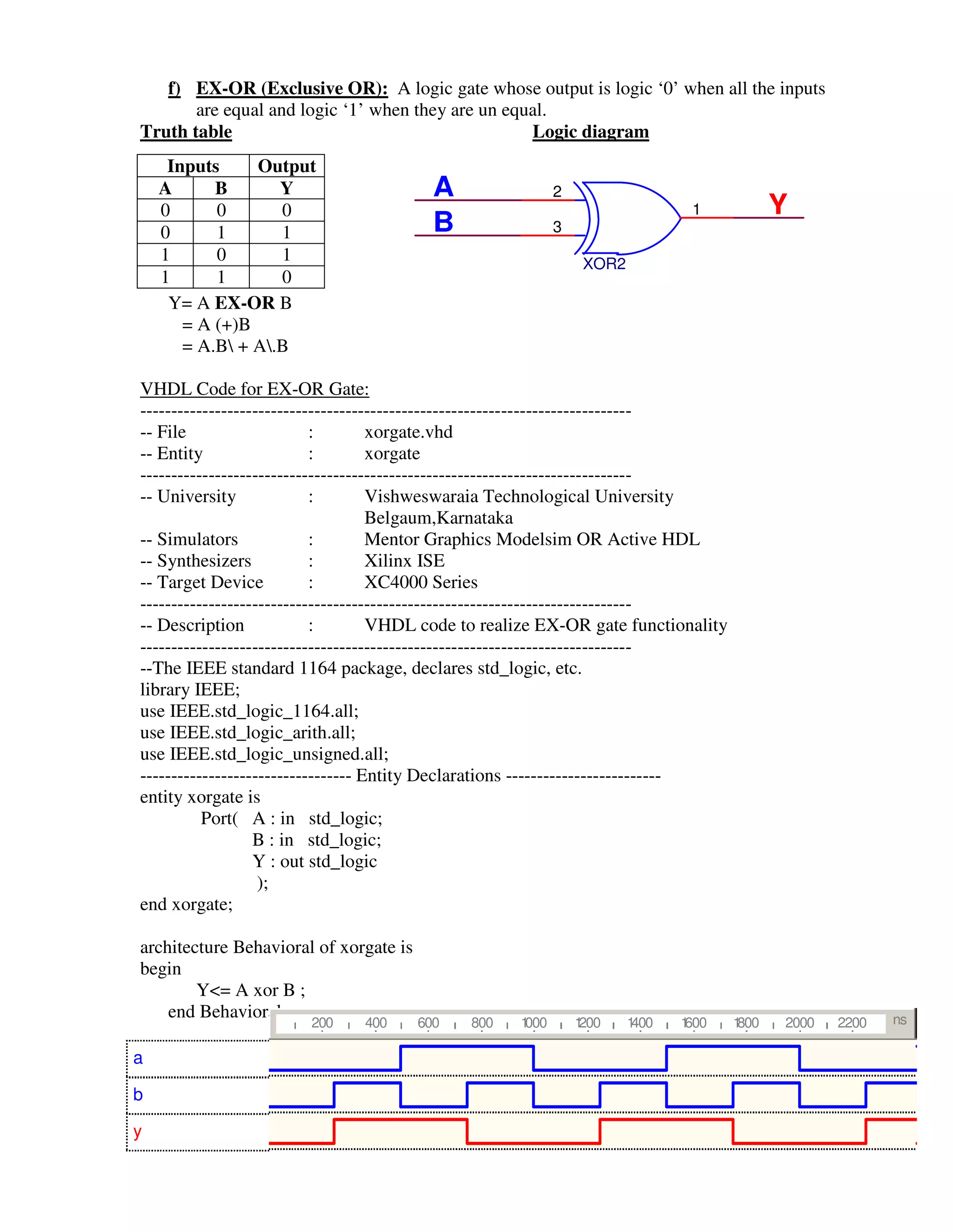
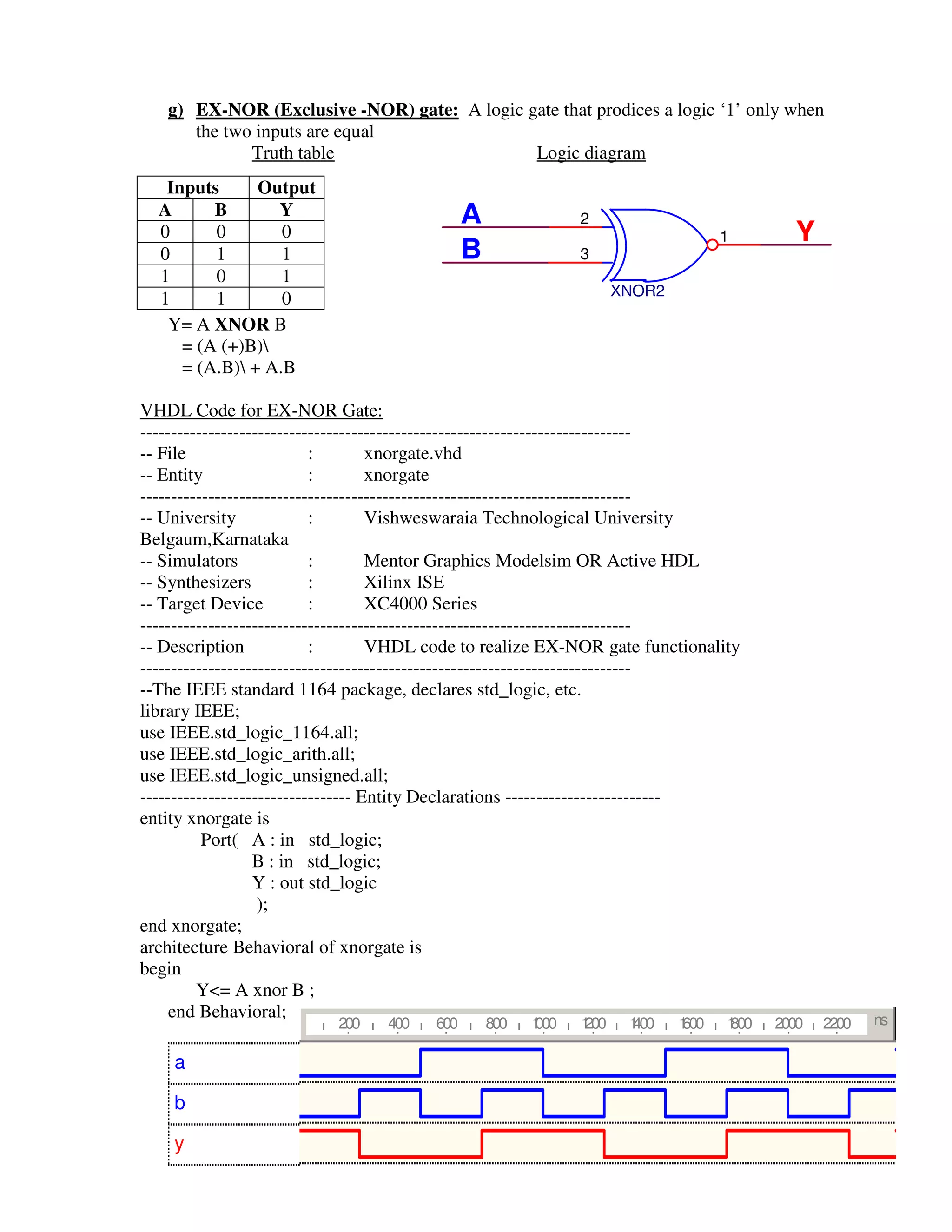
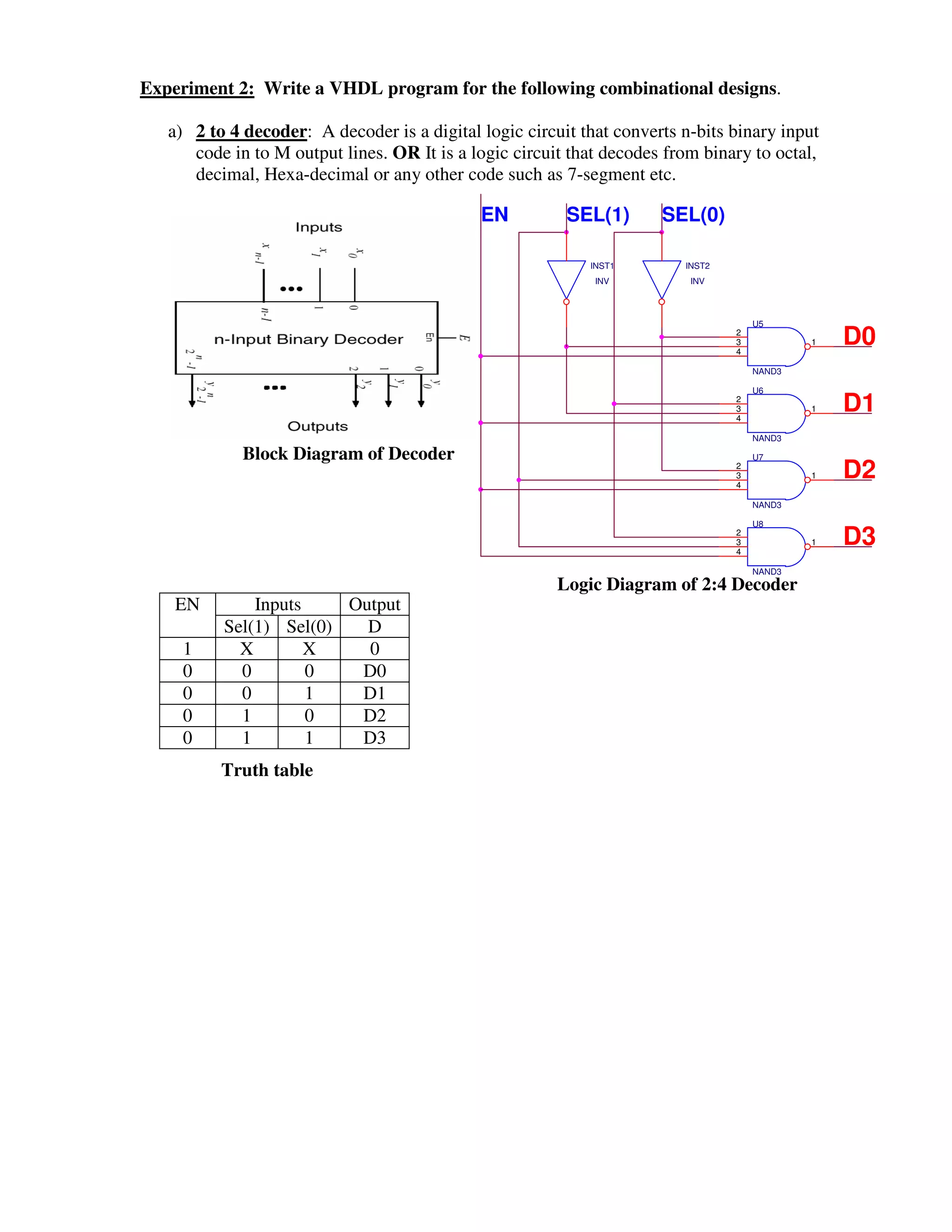
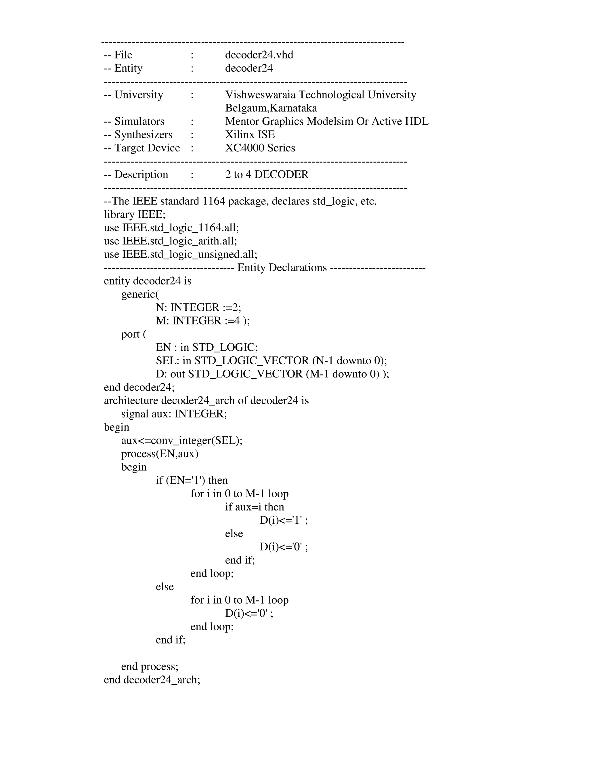
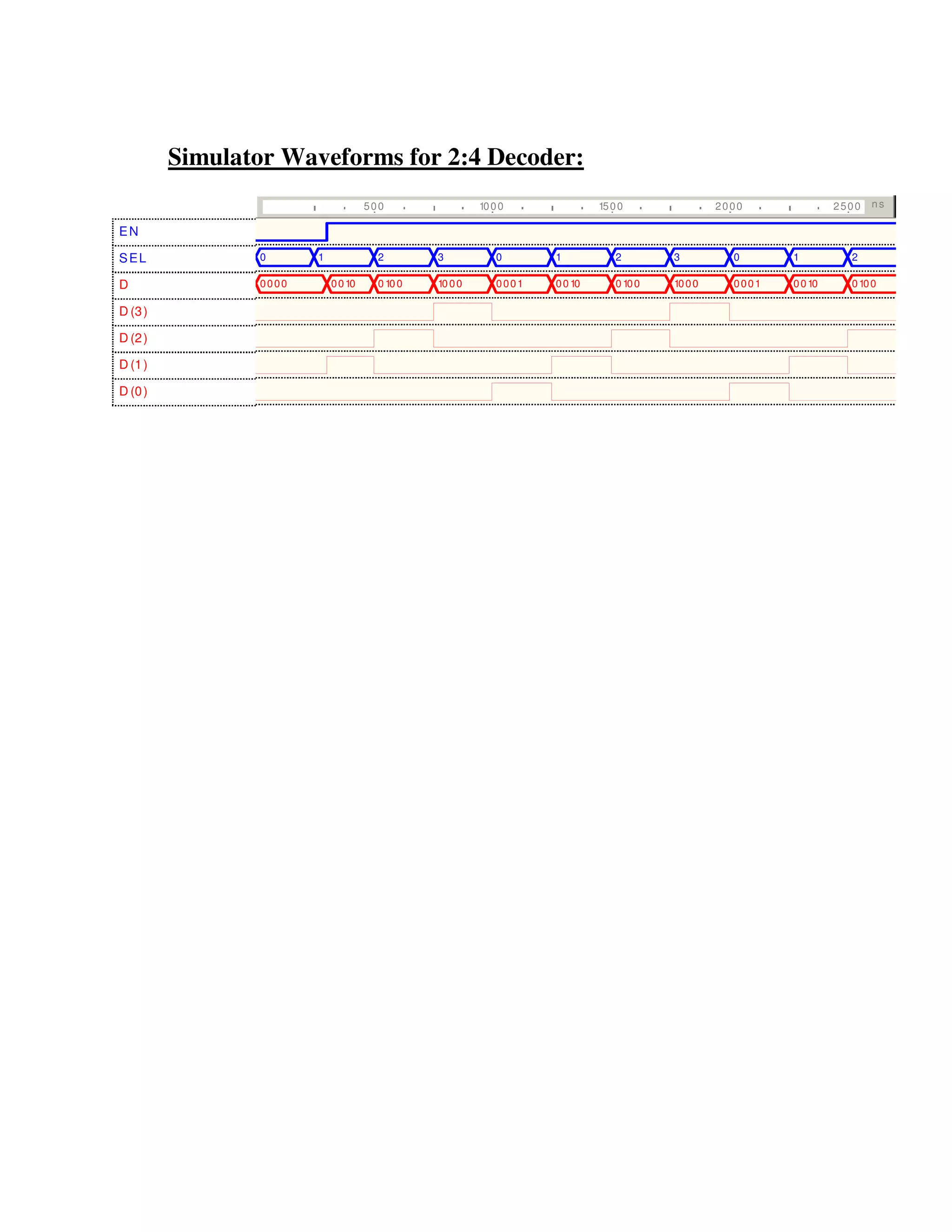
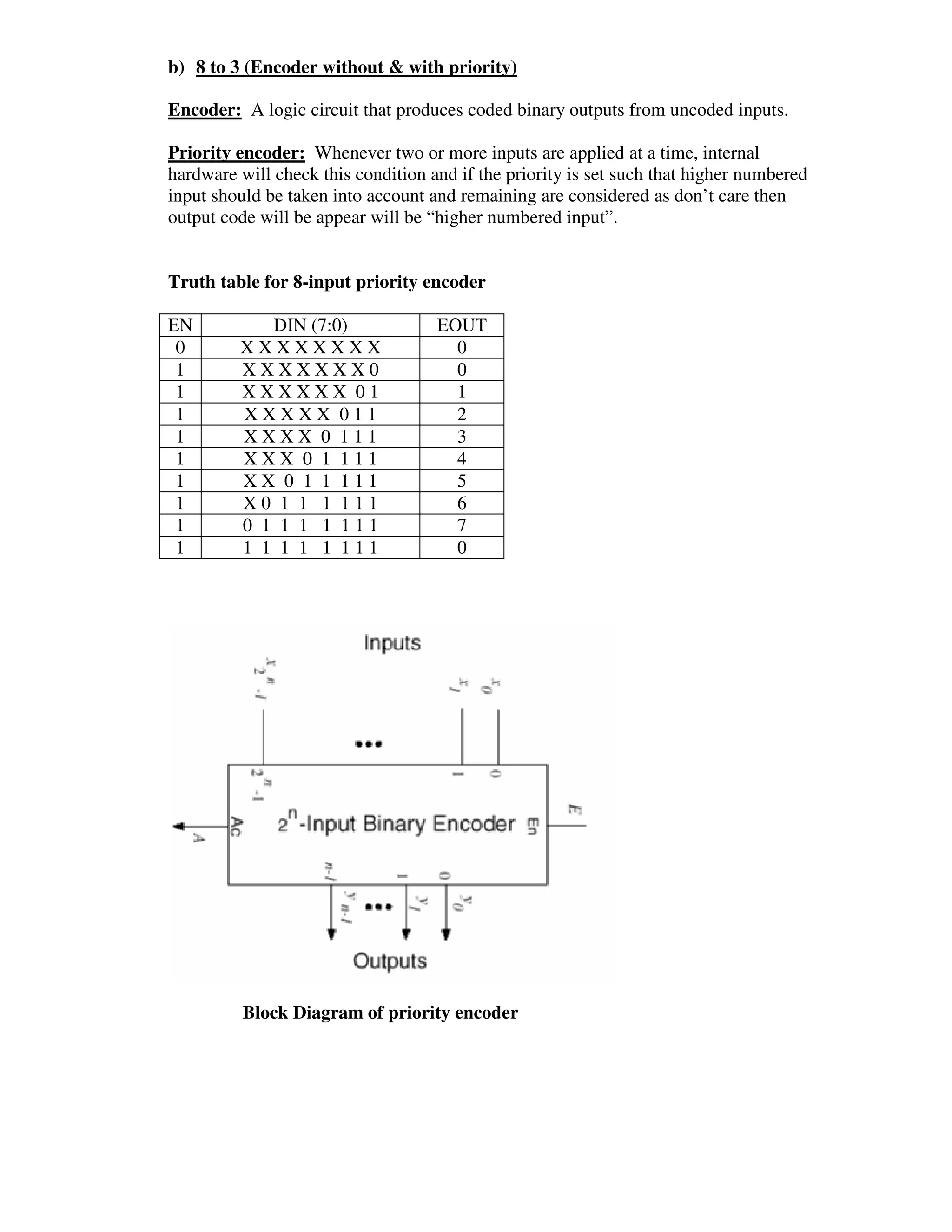
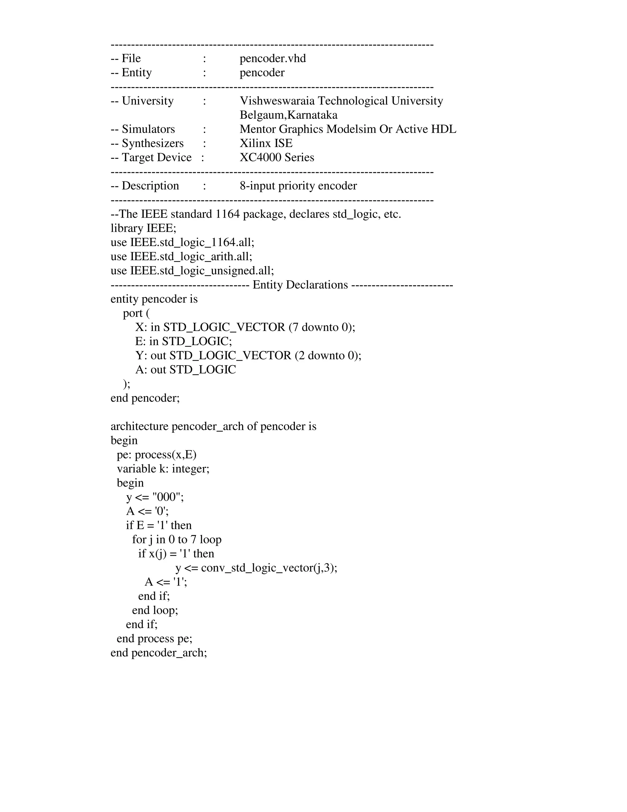
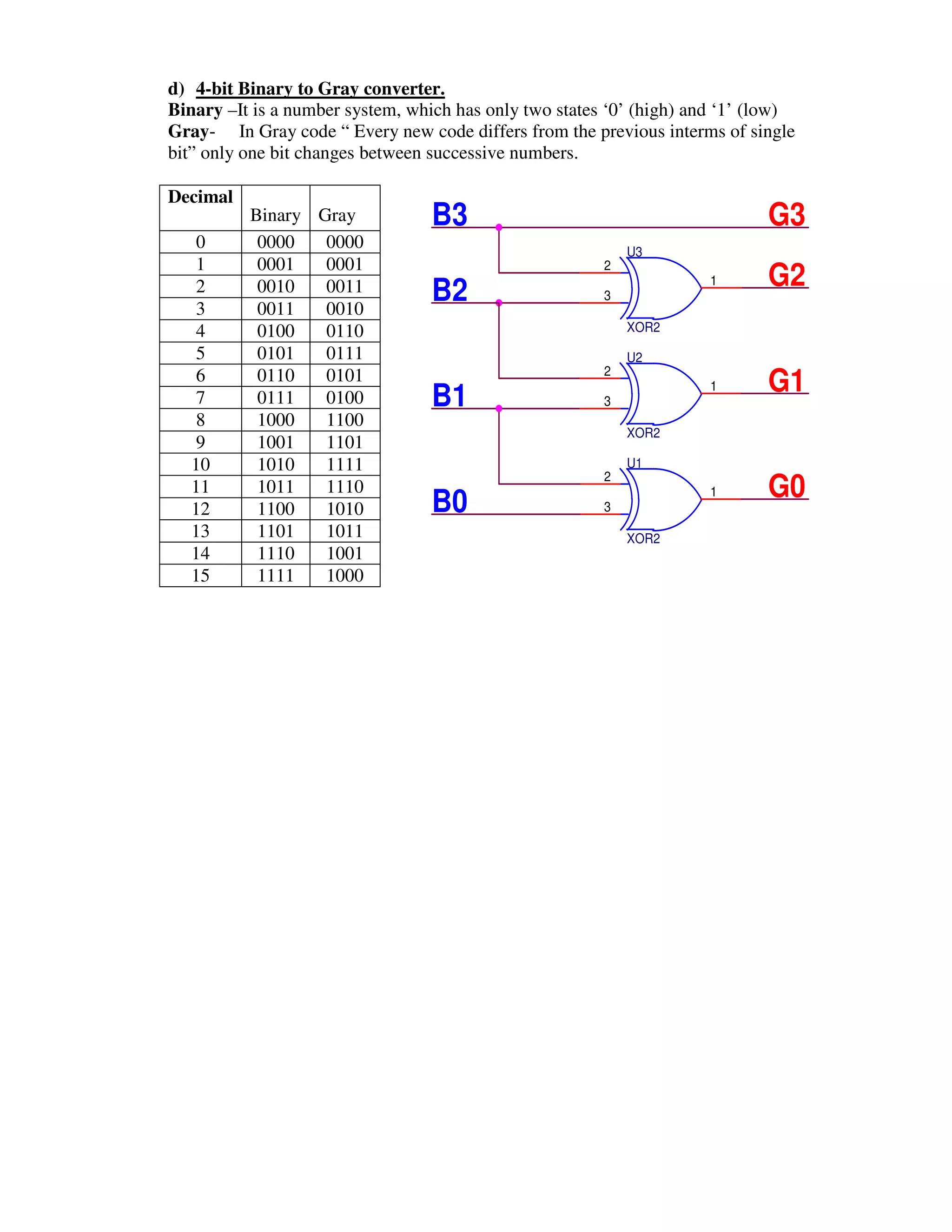
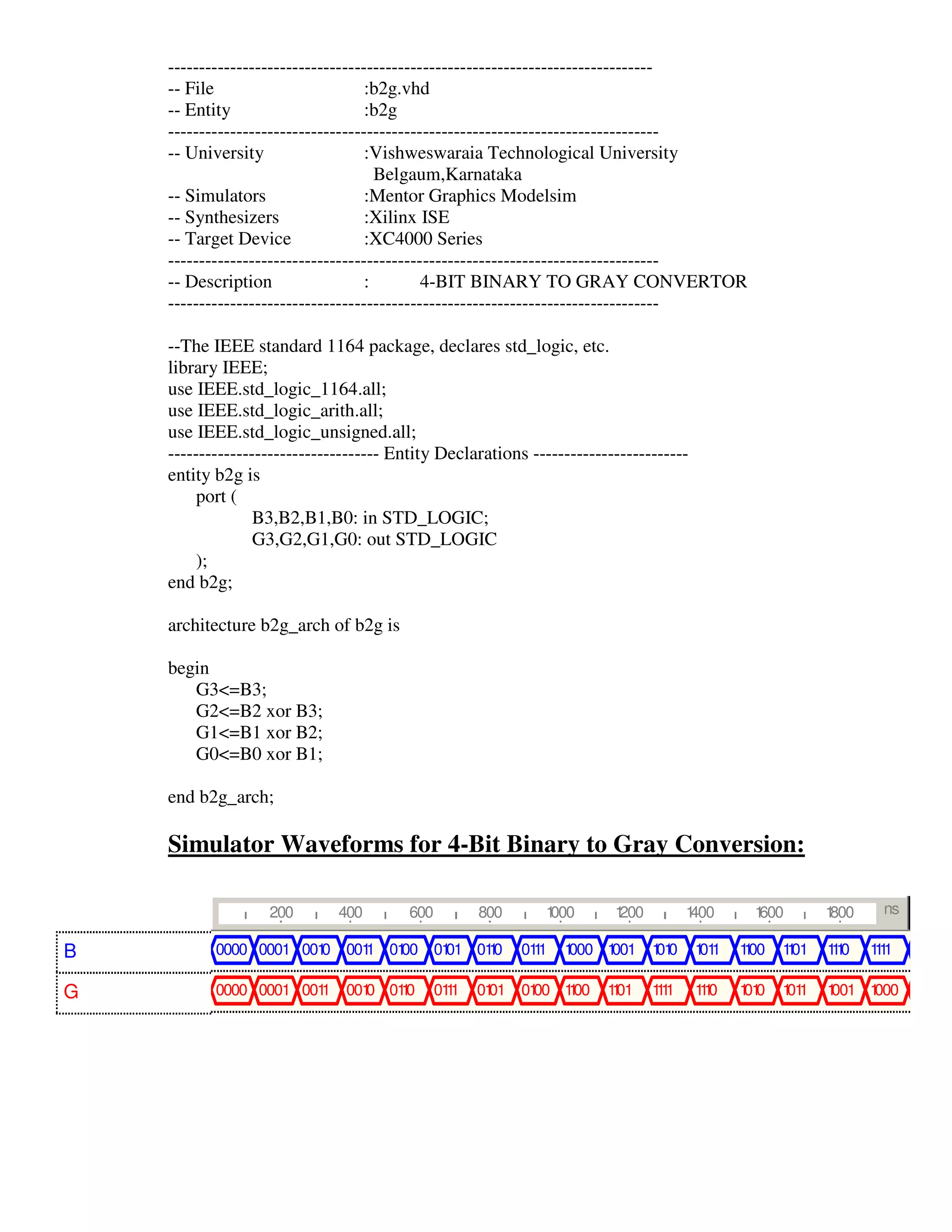
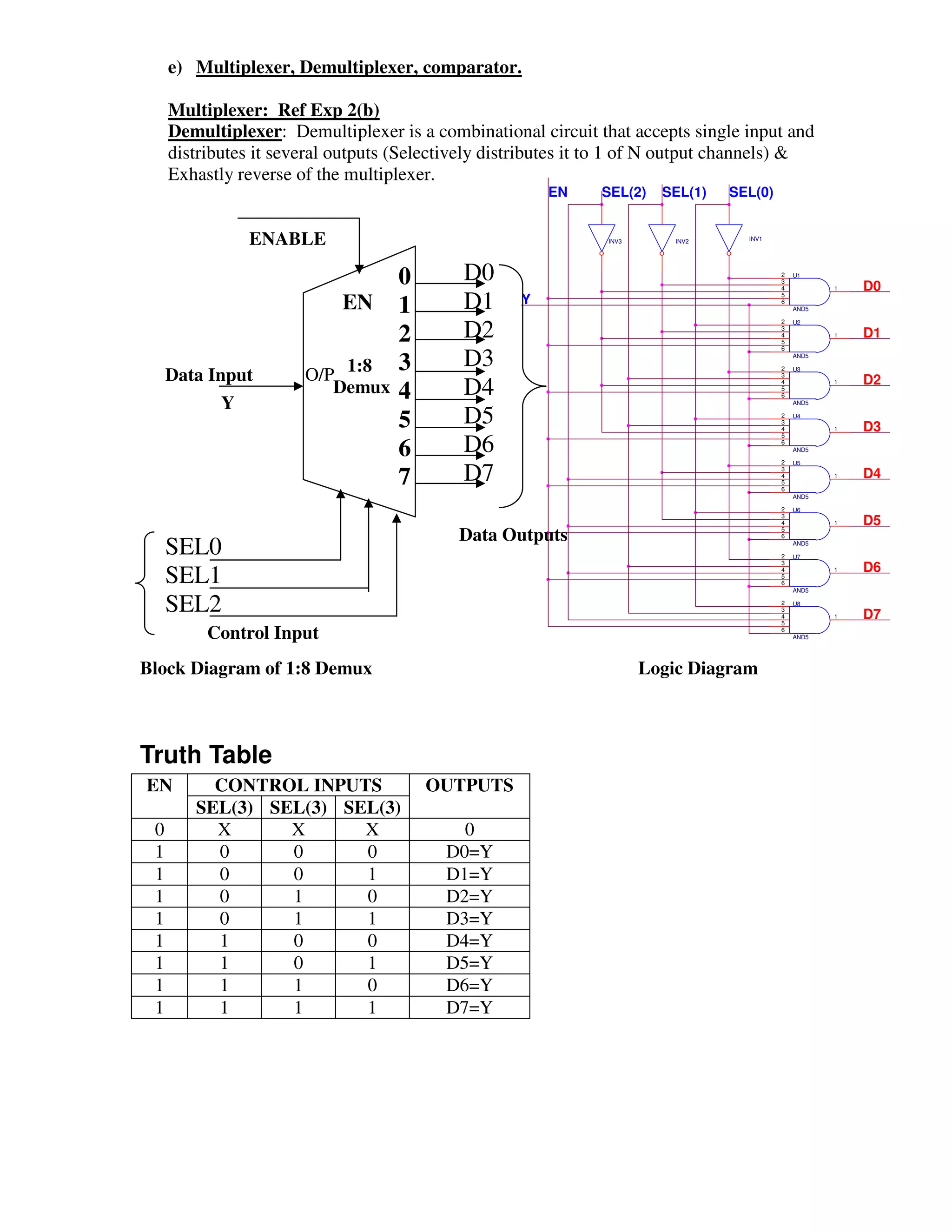
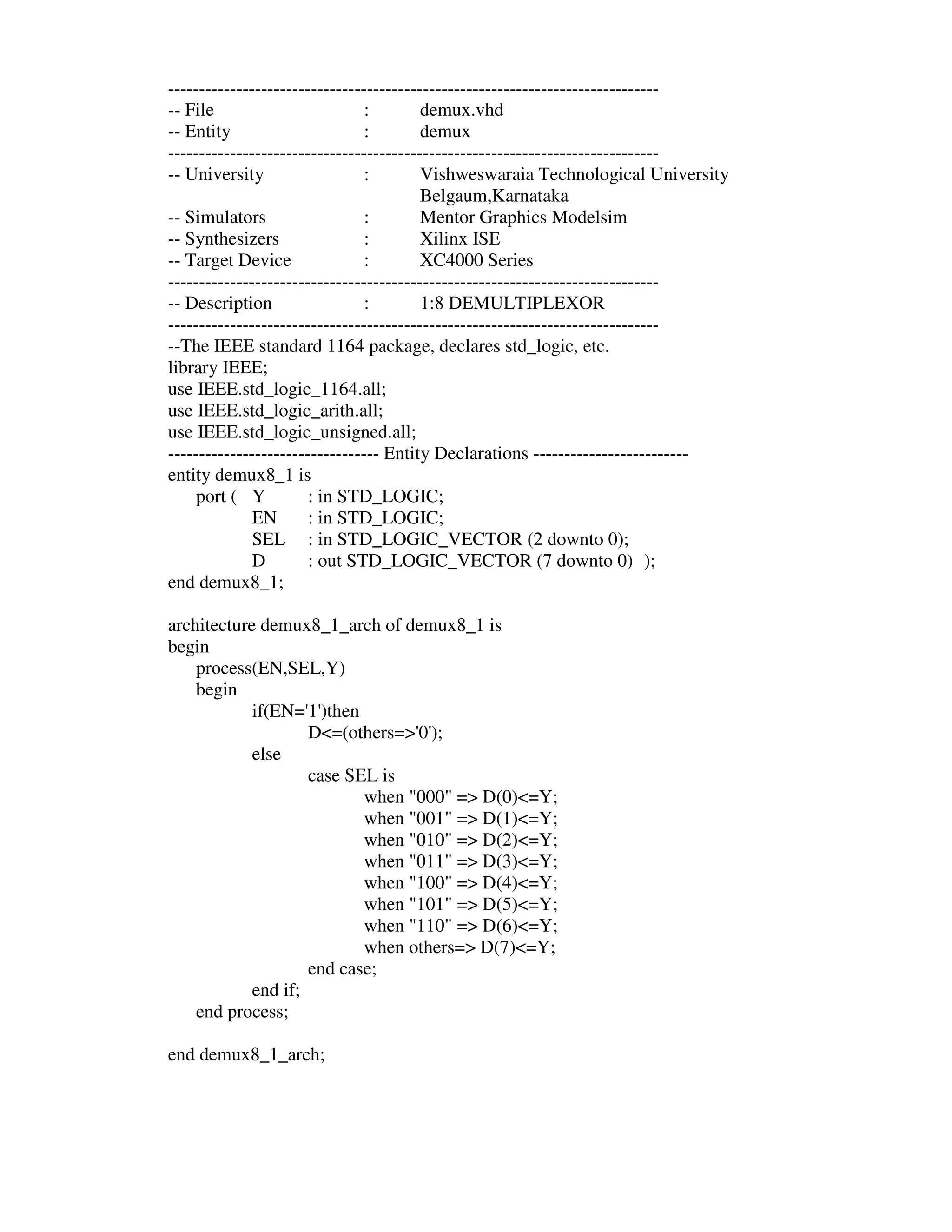
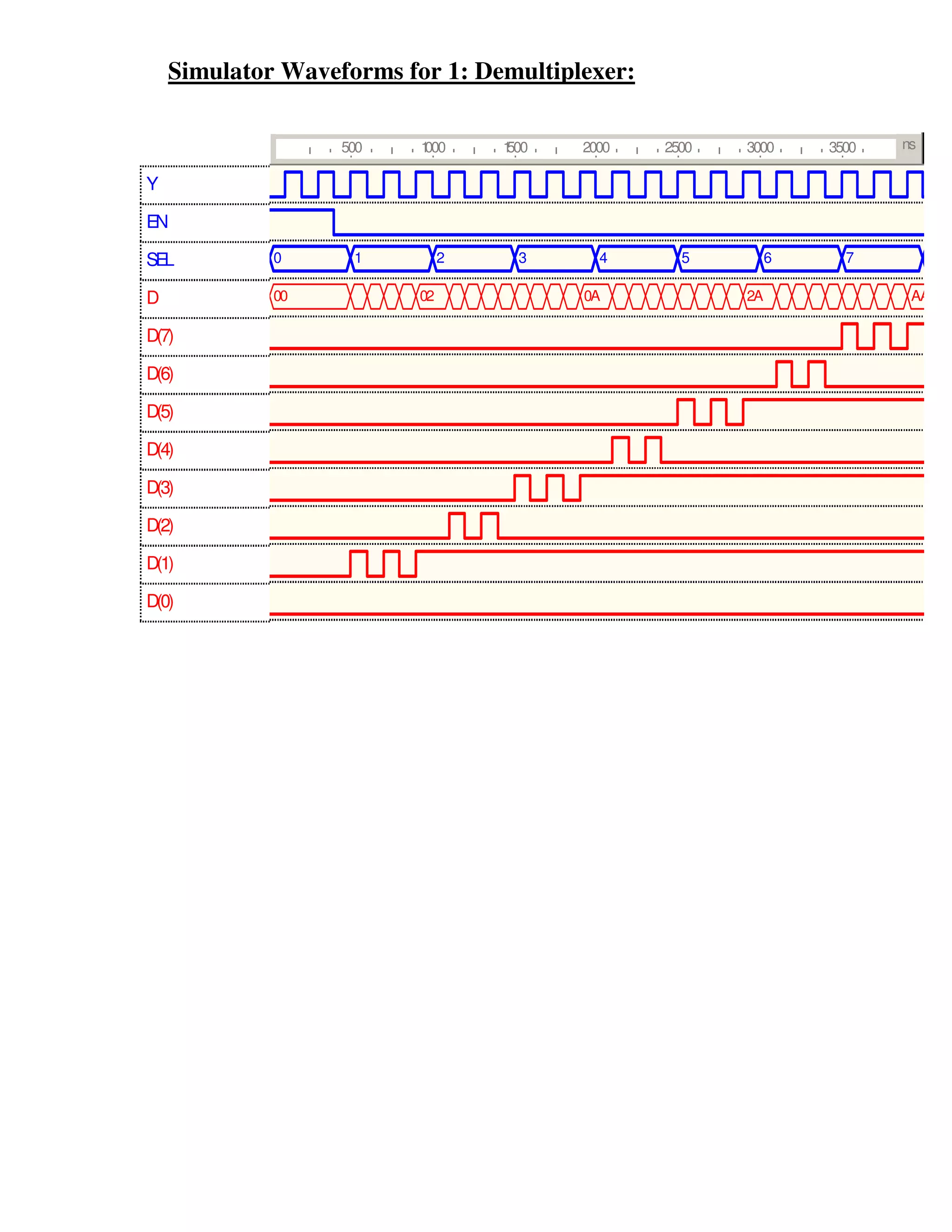
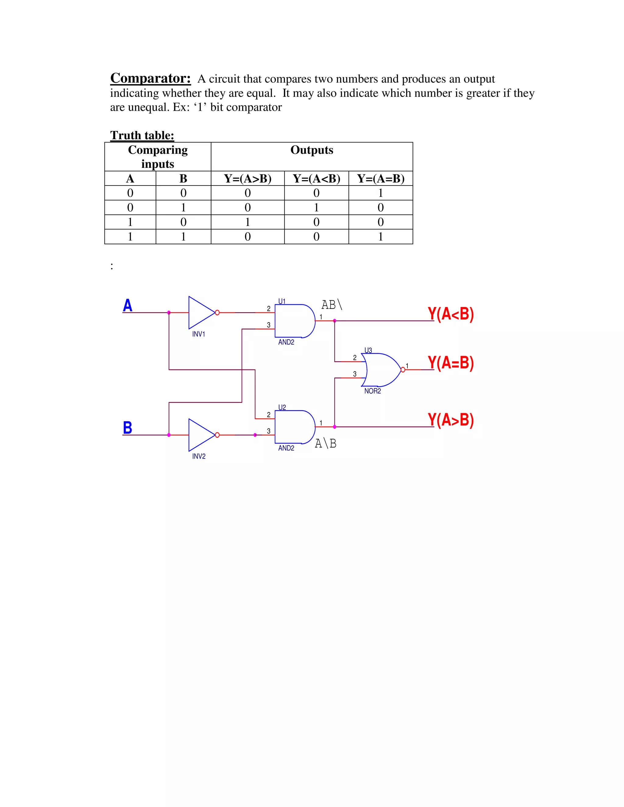
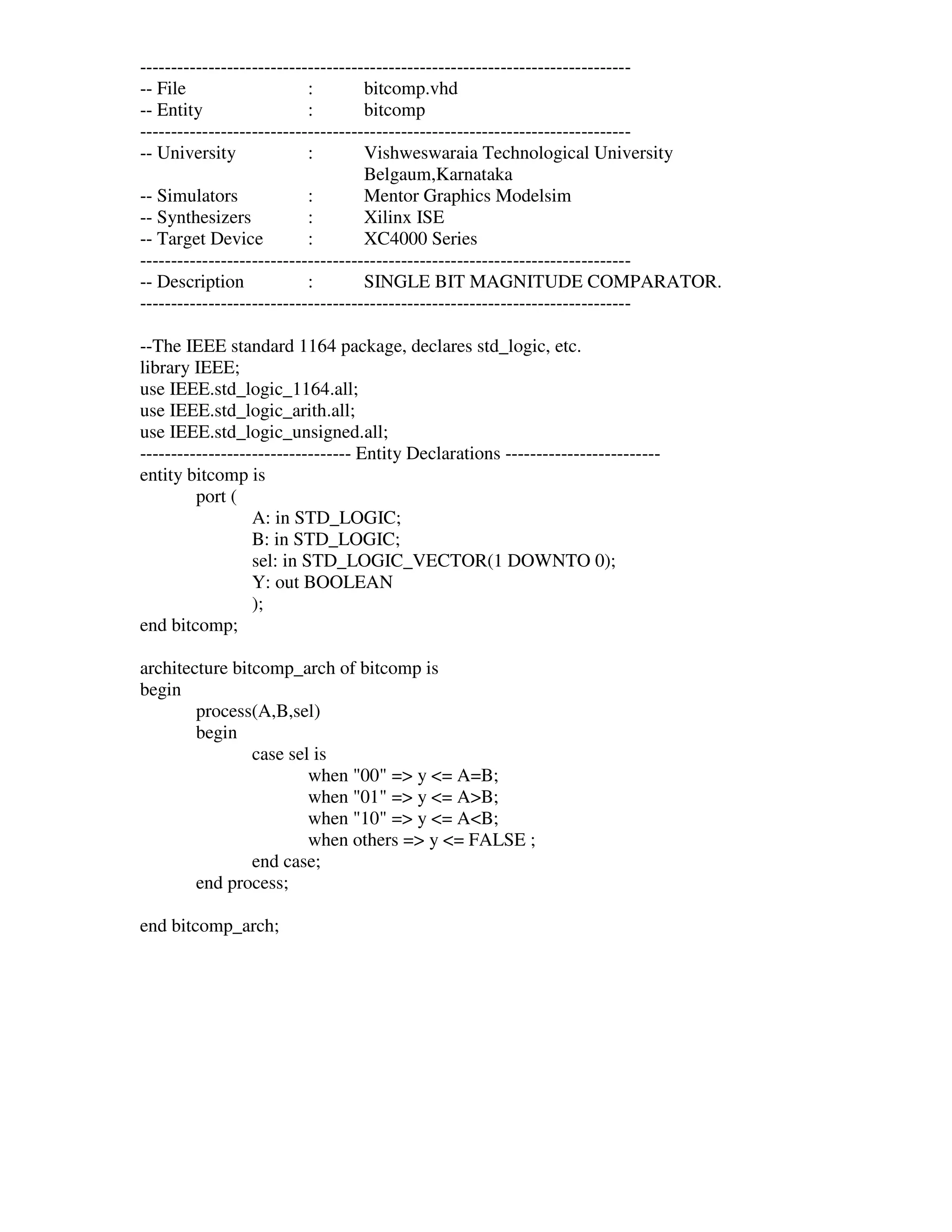
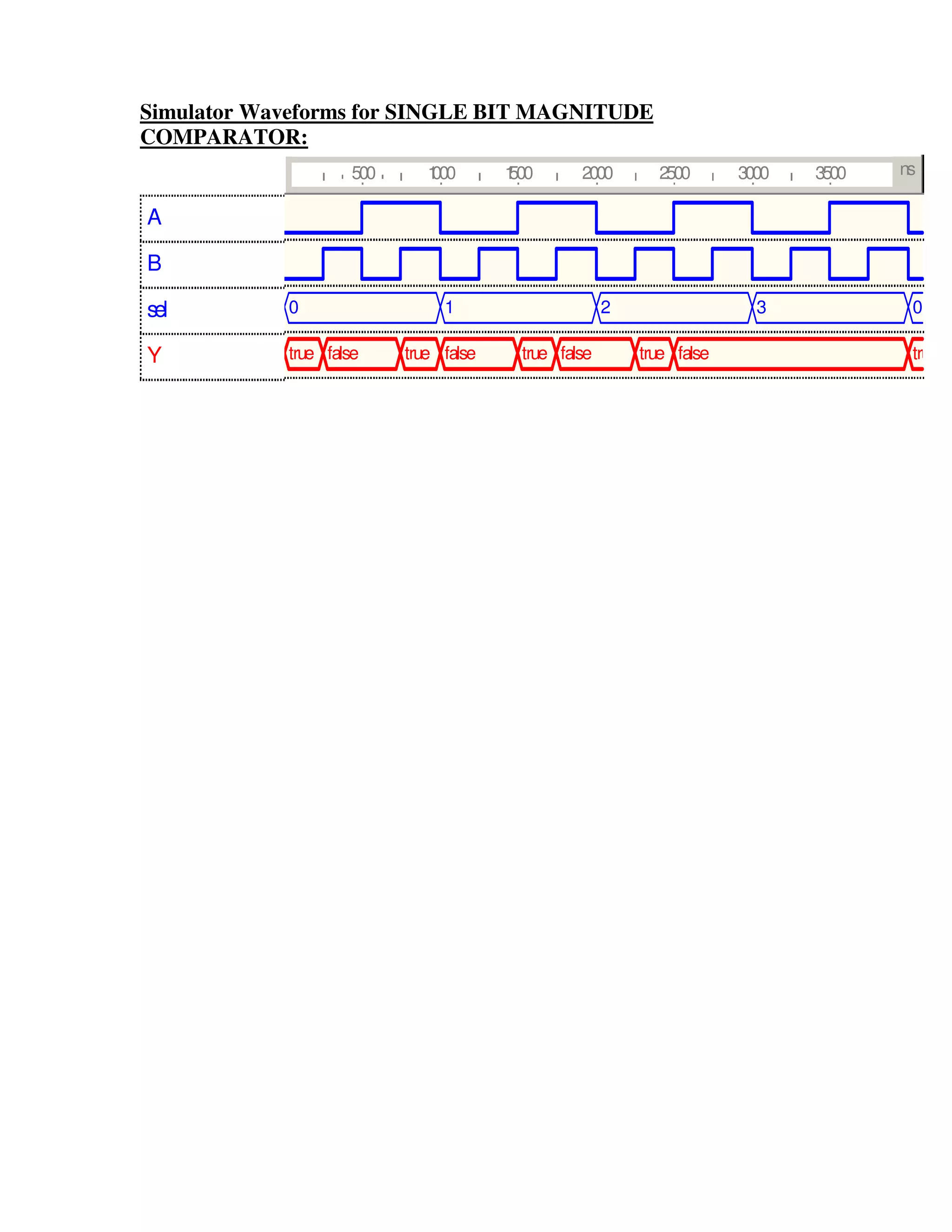
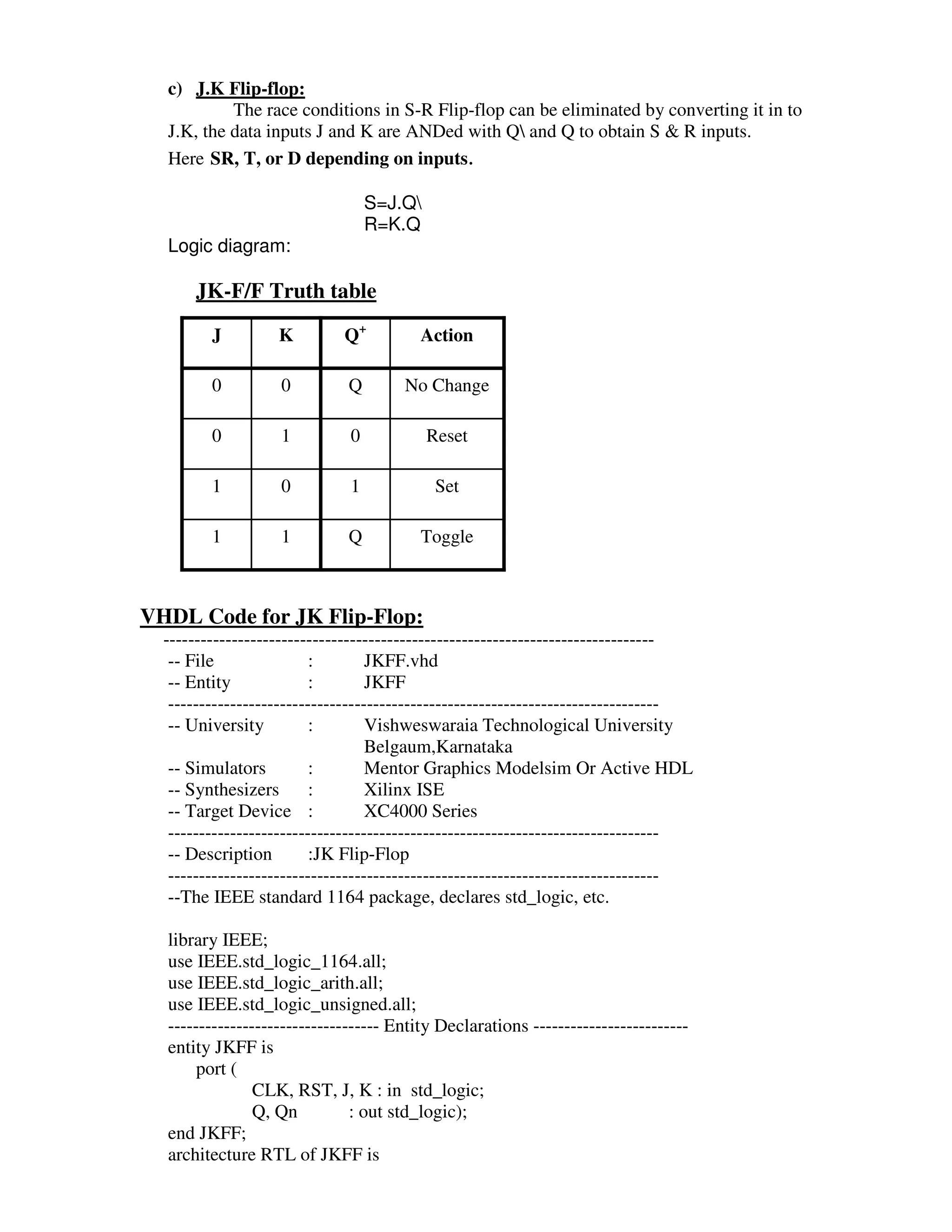
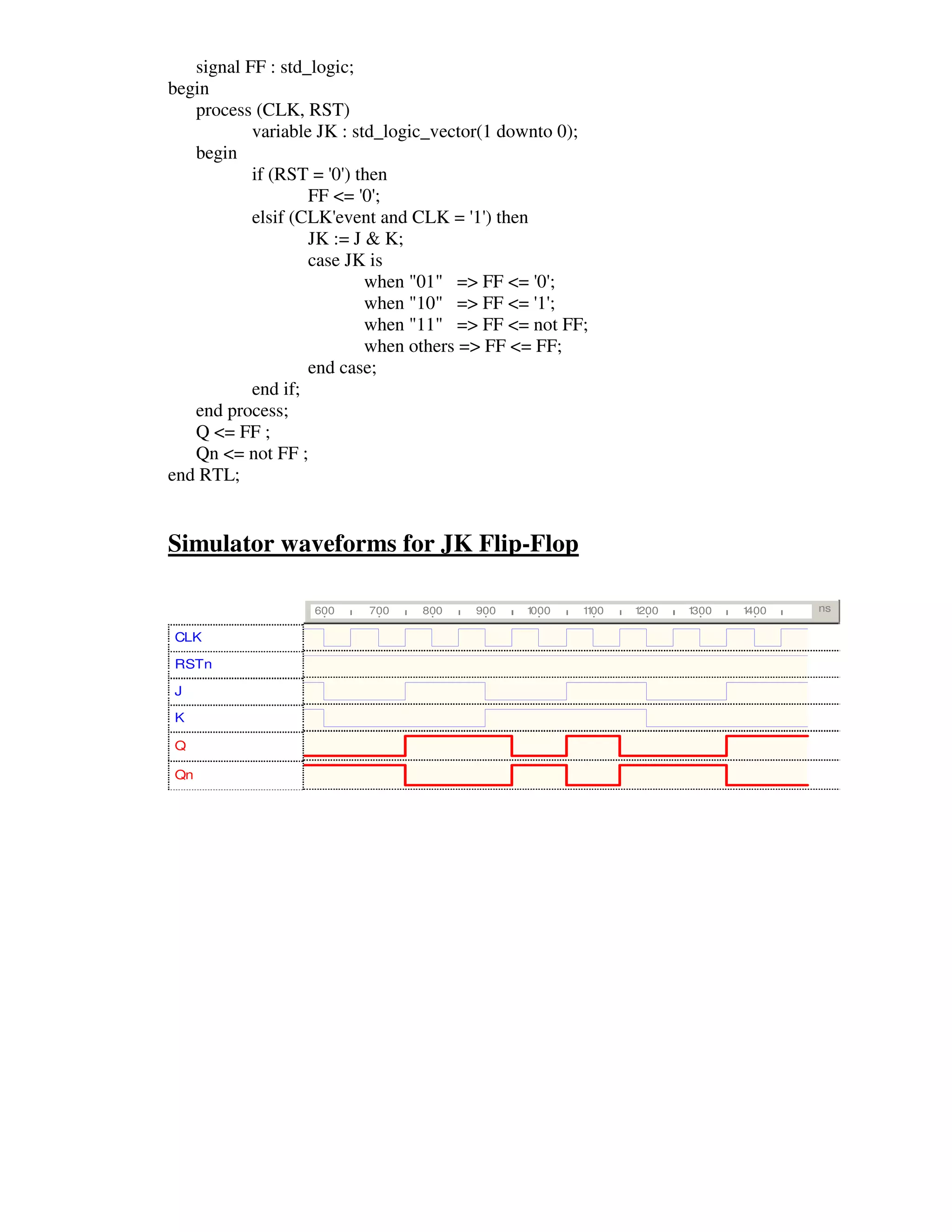
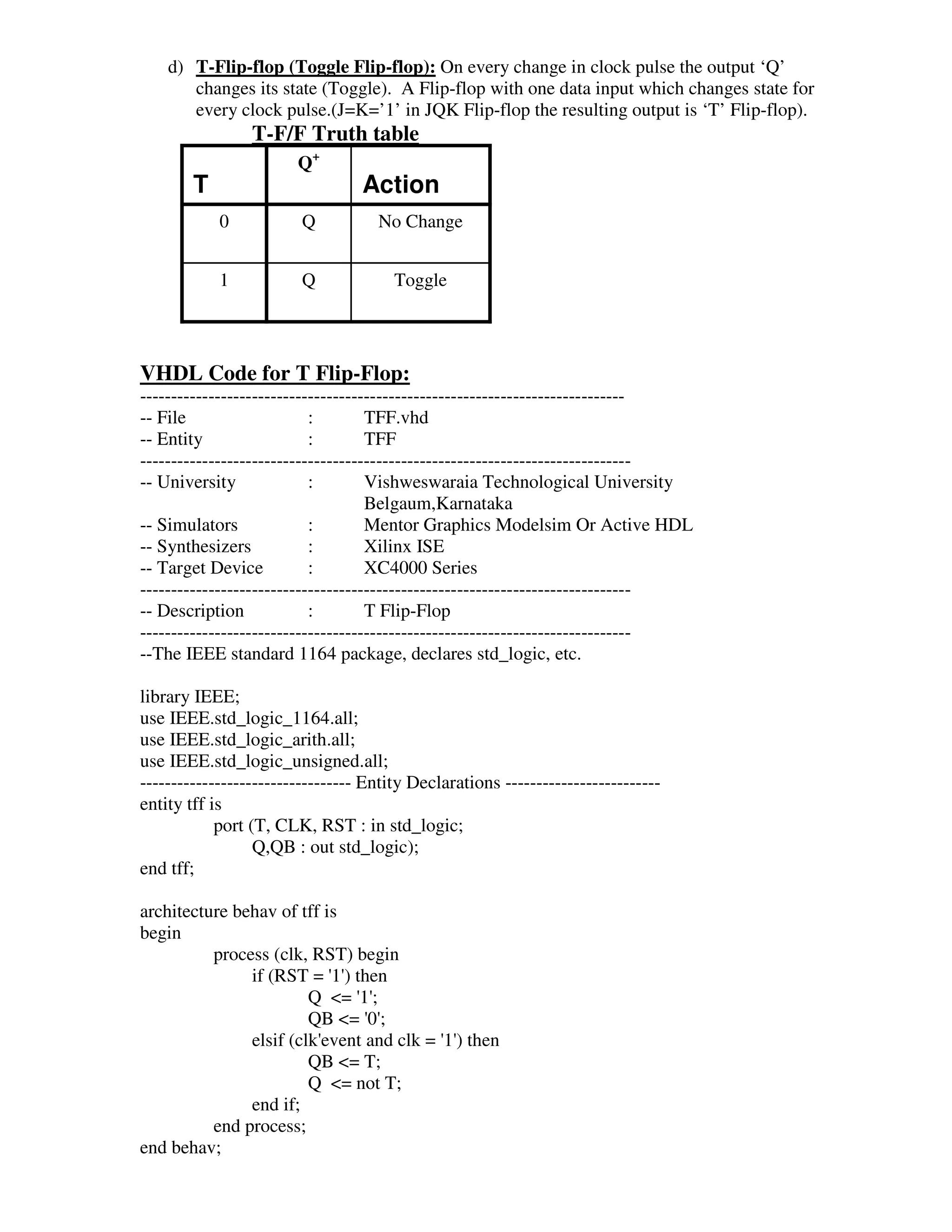
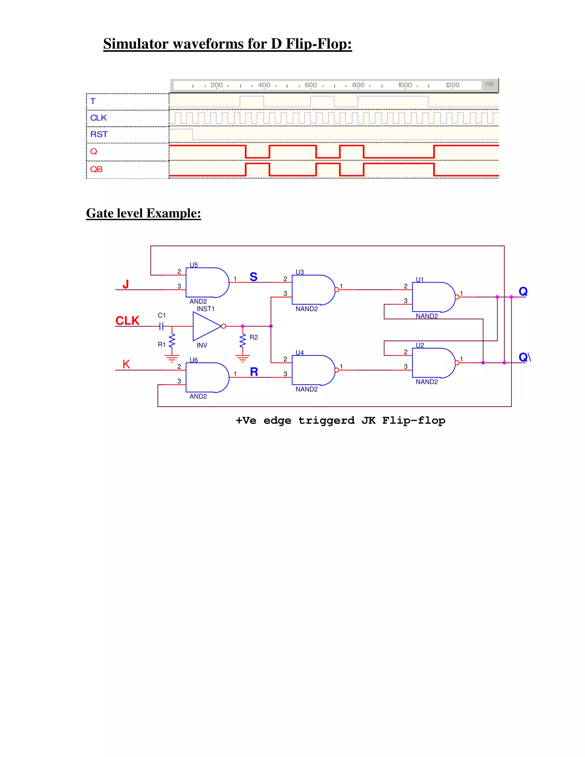
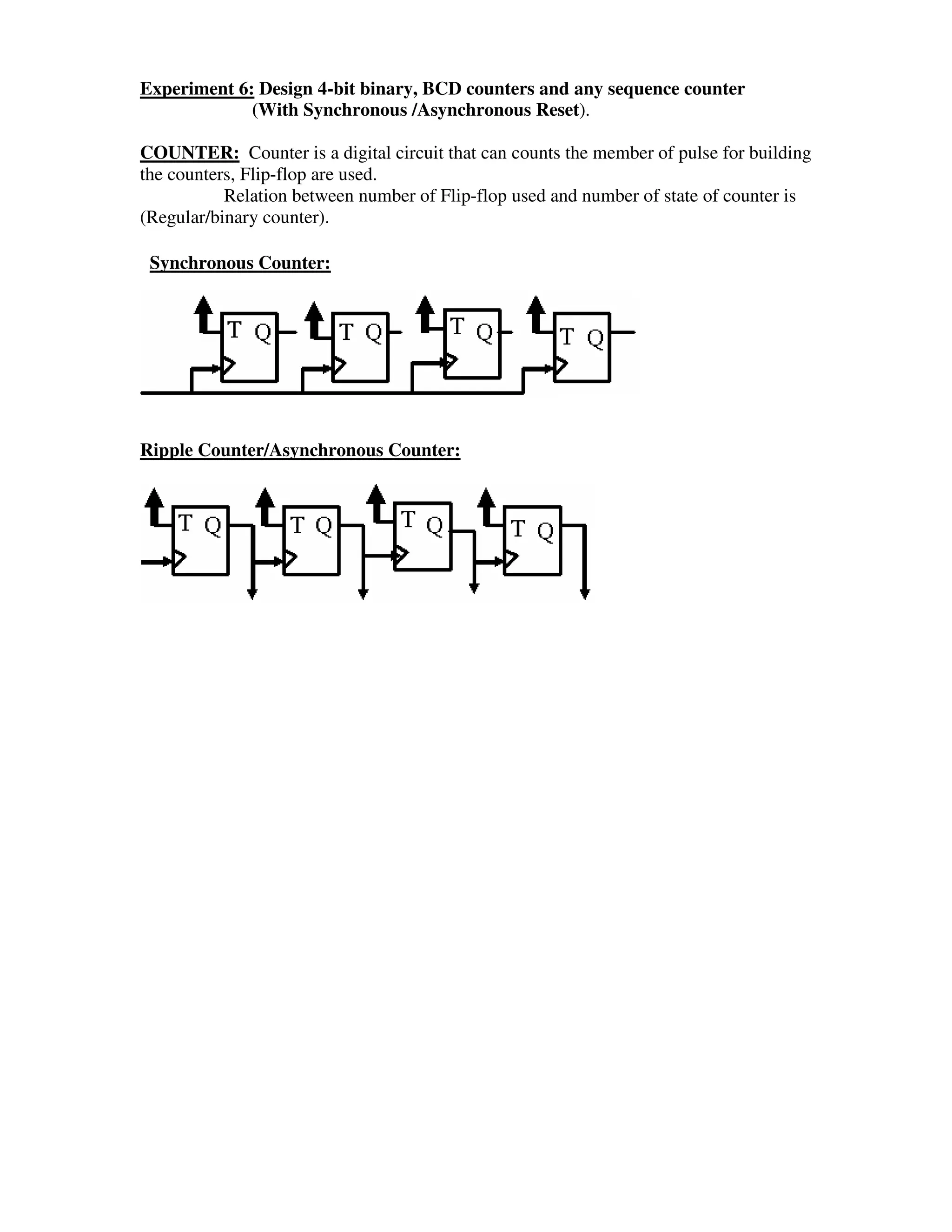
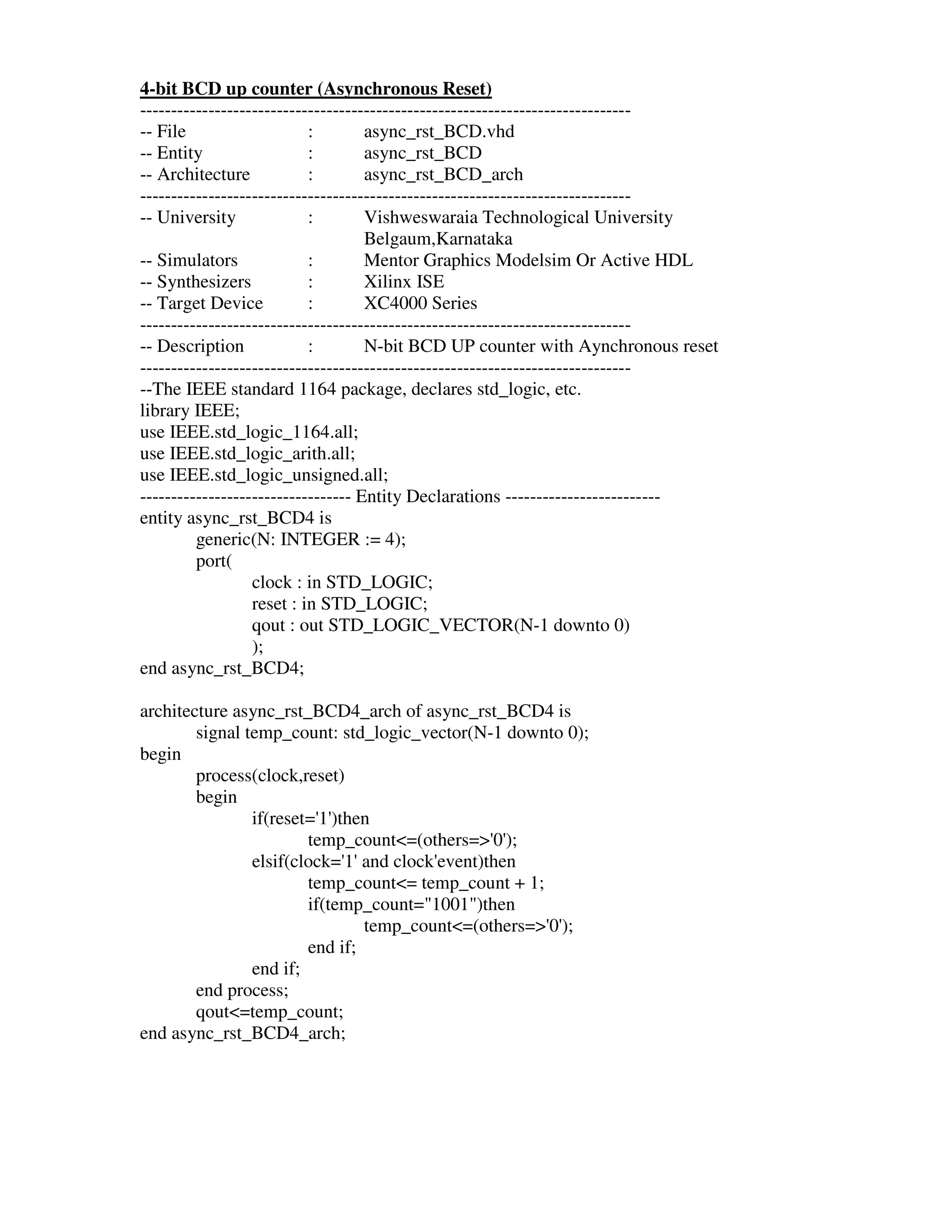
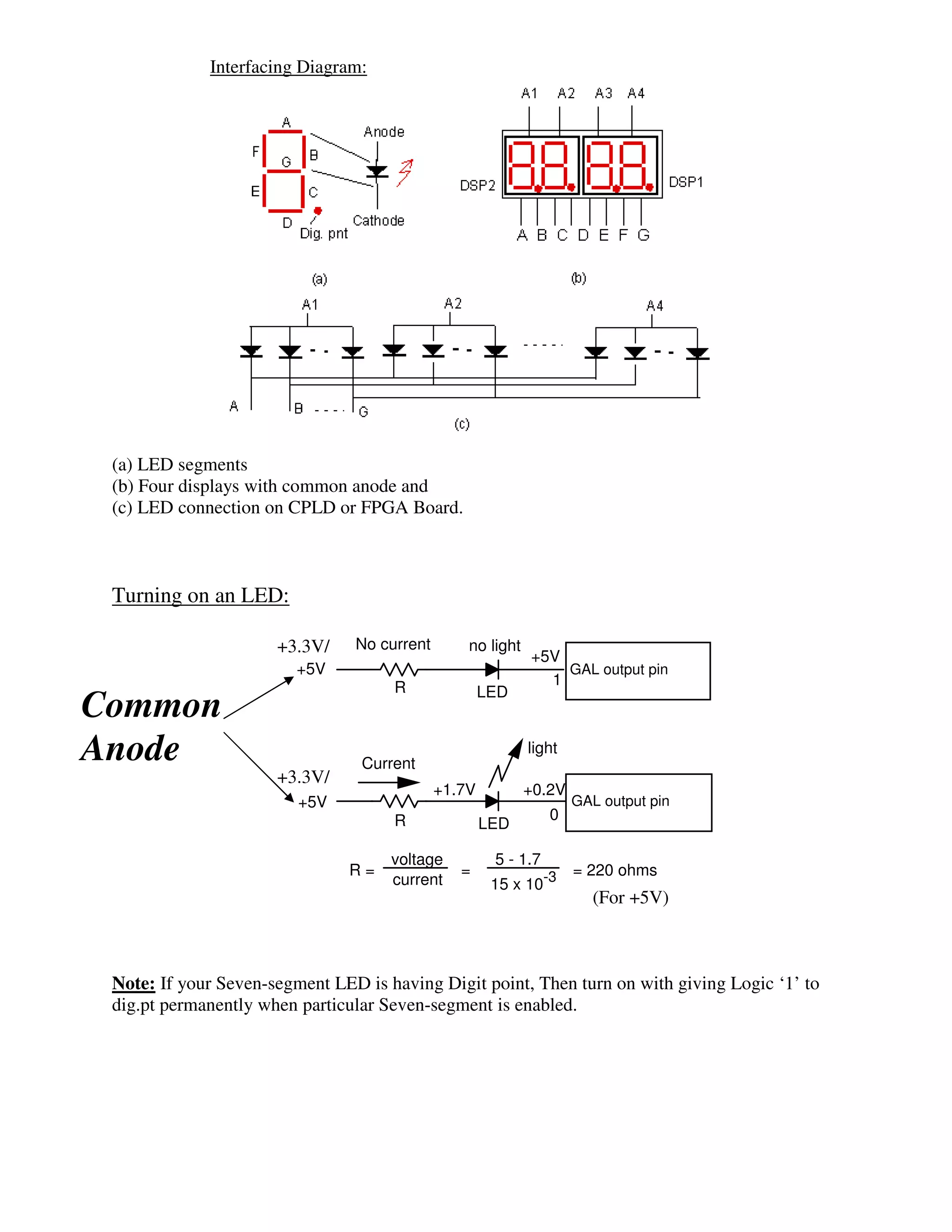
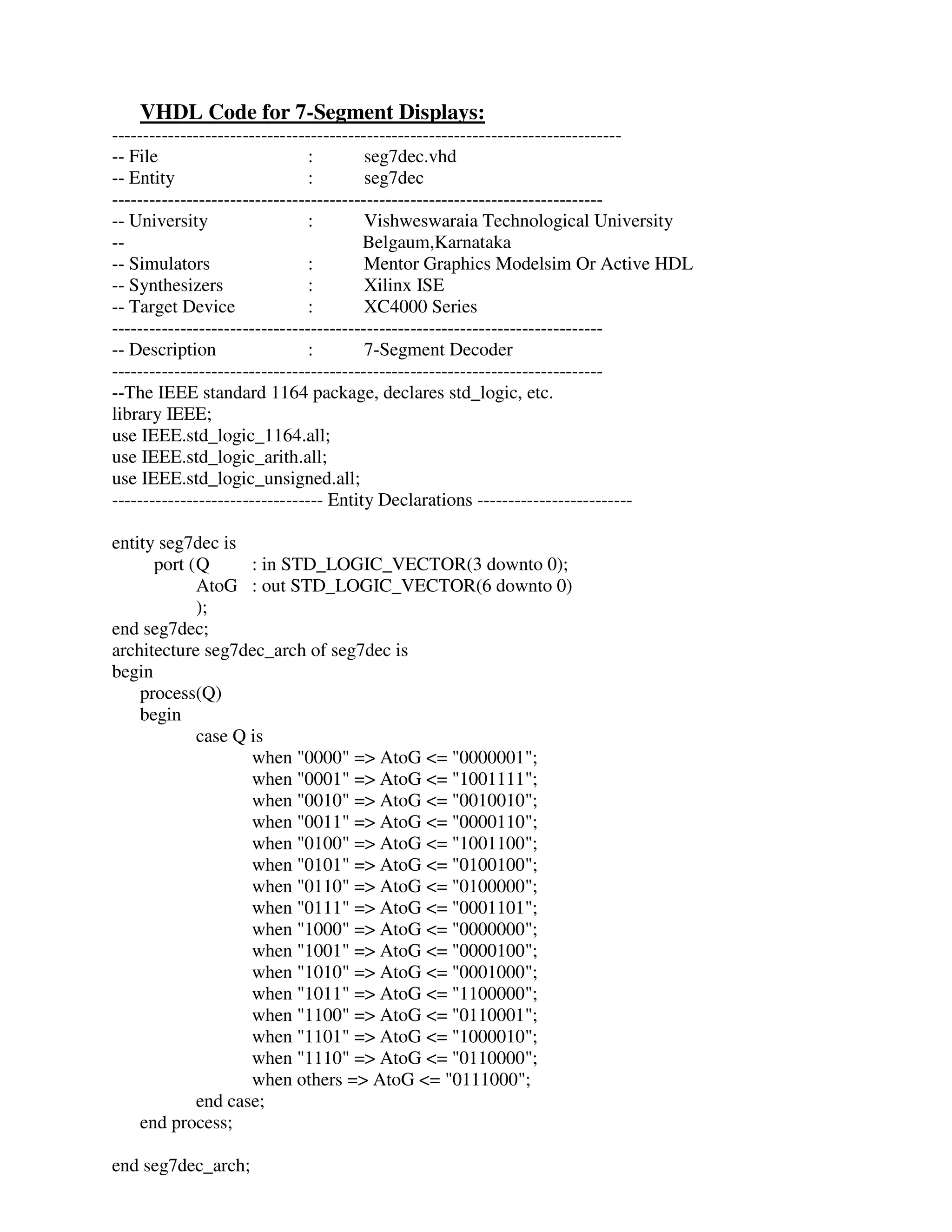
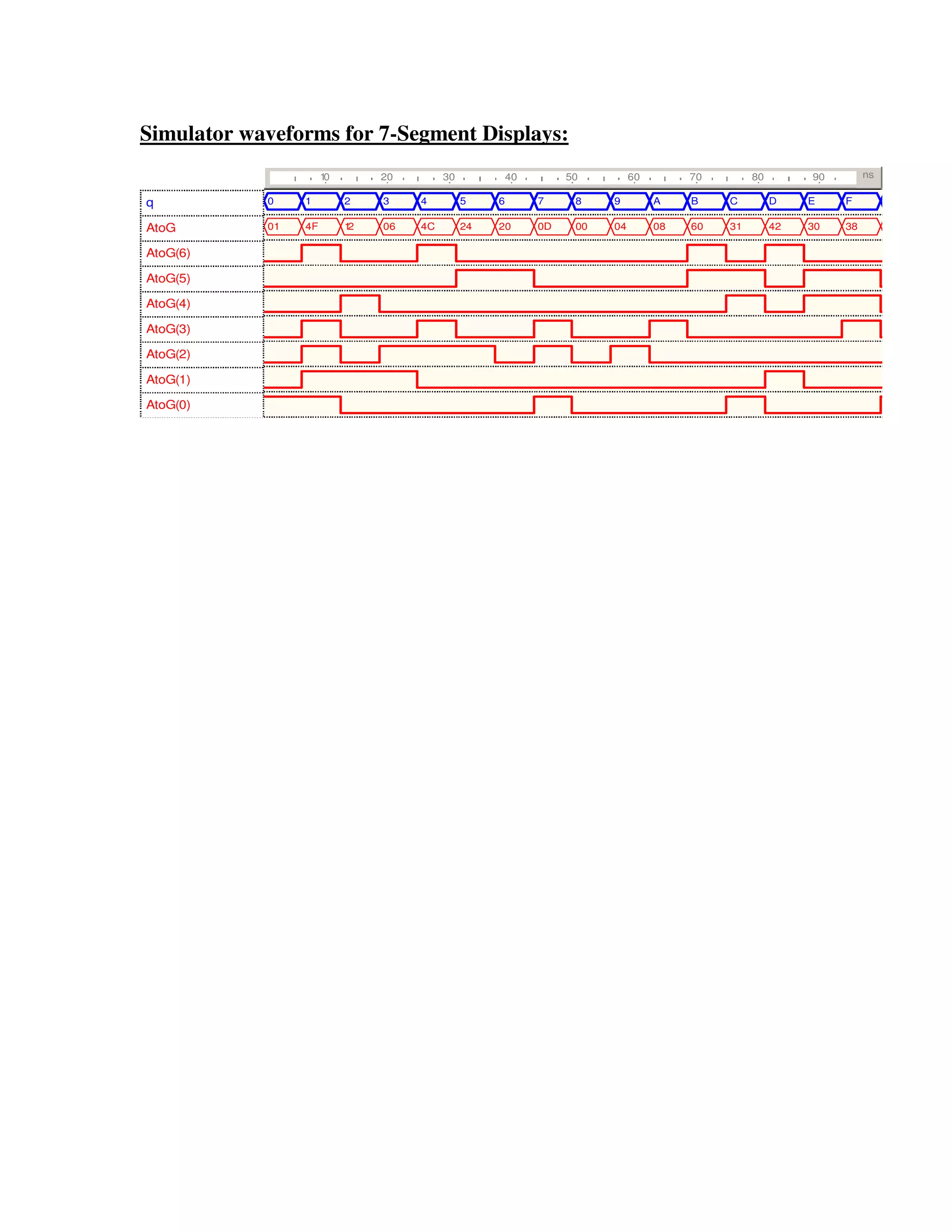
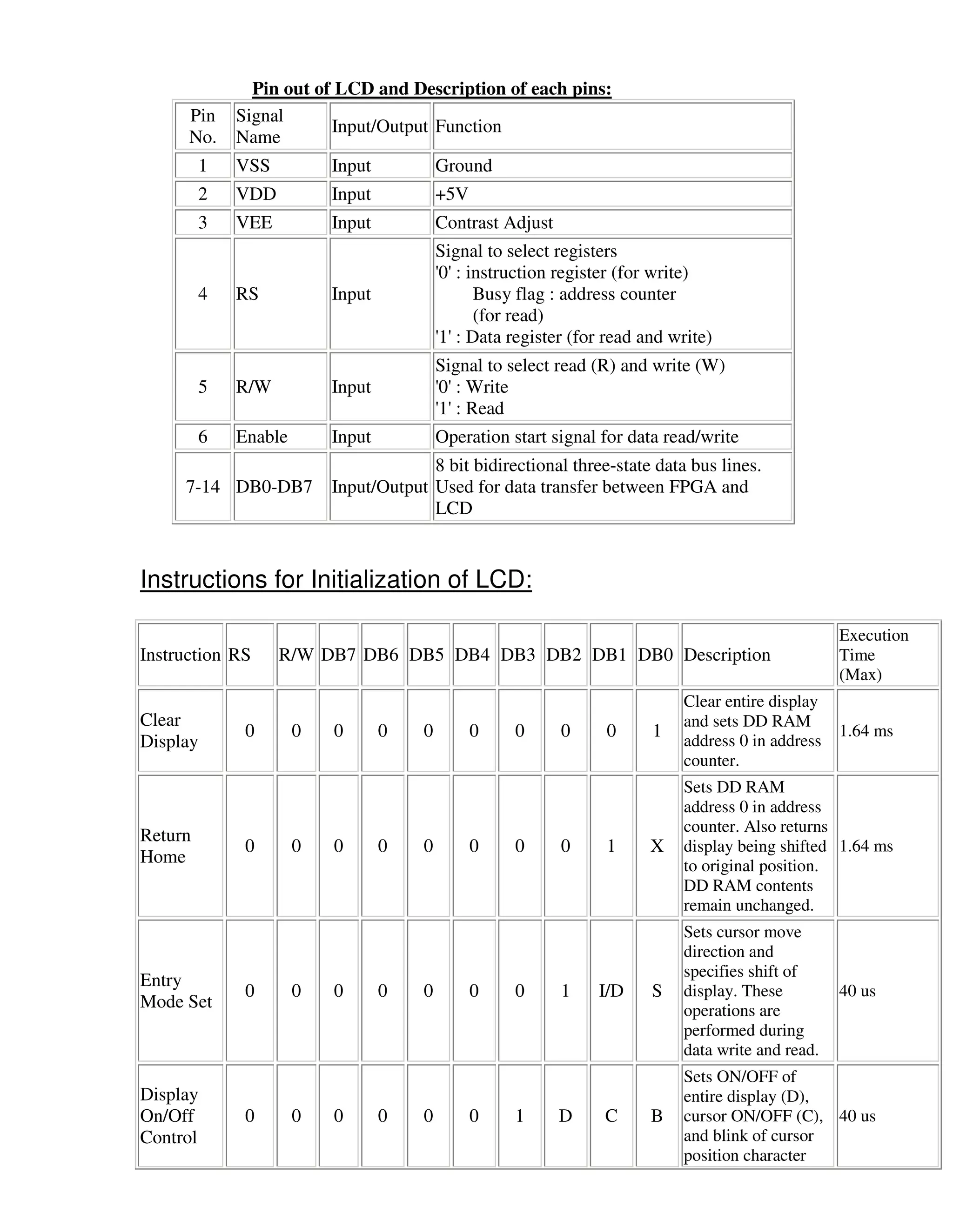
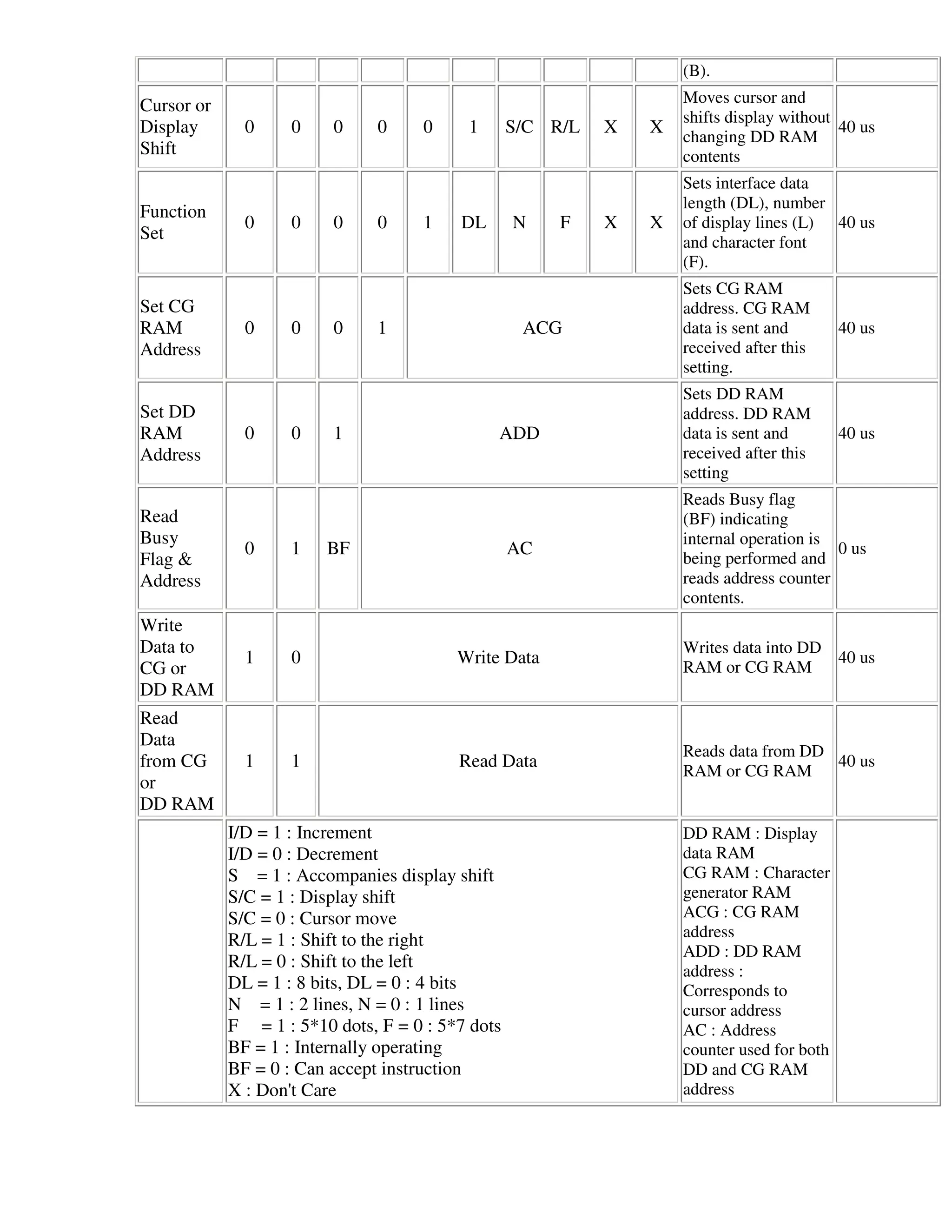
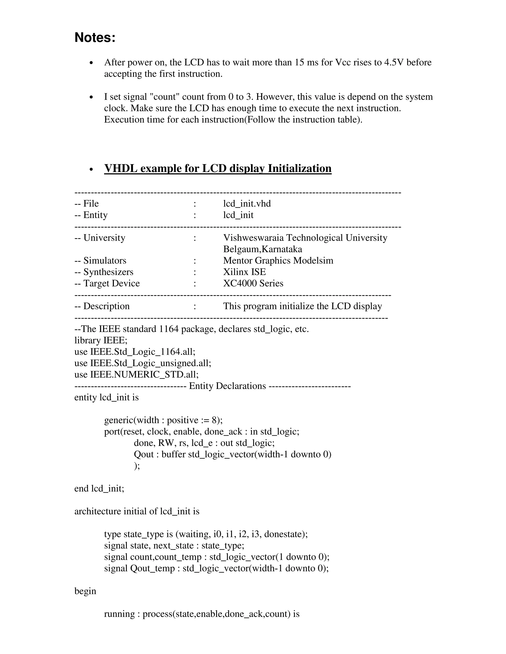
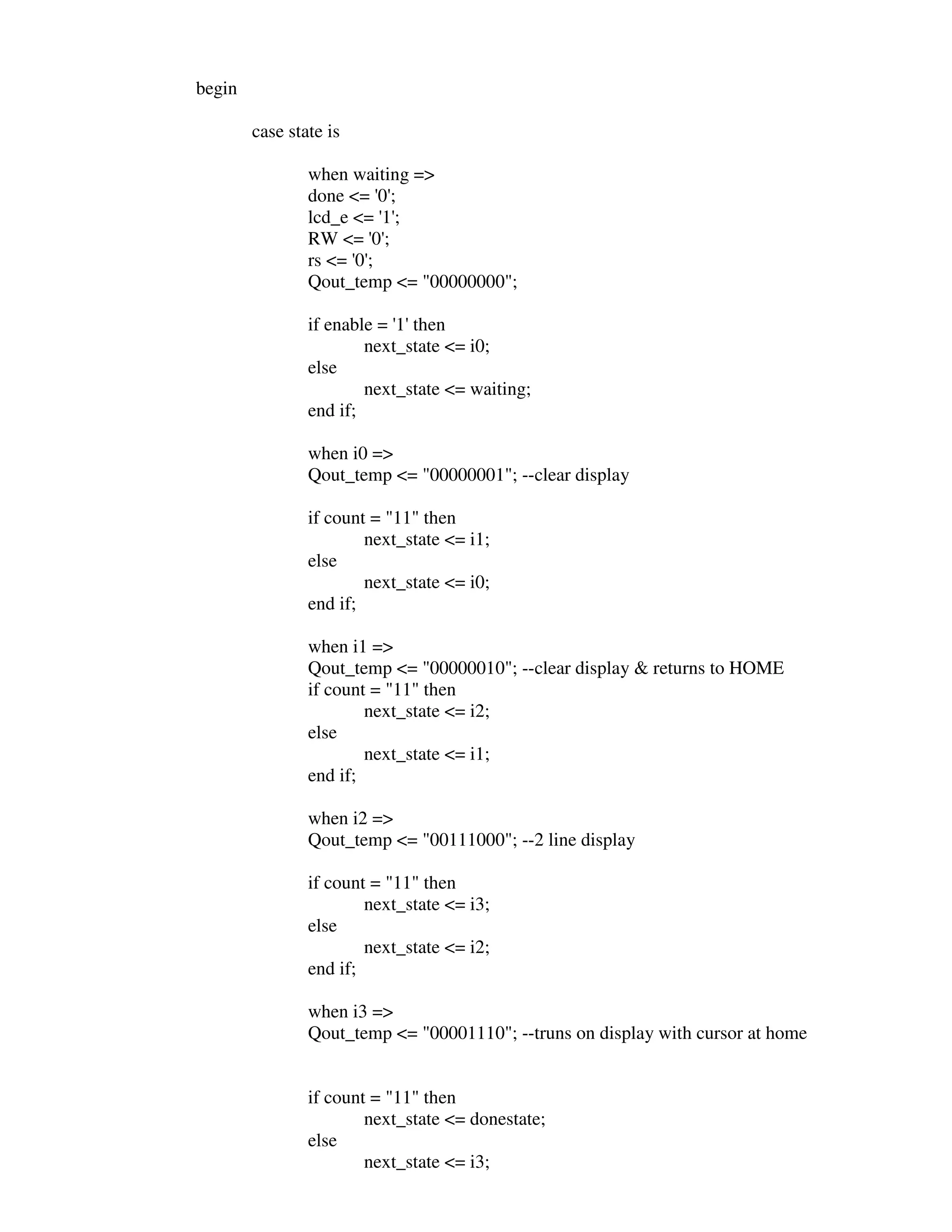
The document describes an experiment to write VHDL code for basic logic gates. It includes the truth tables, logic diagrams, and VHDL code for AND, OR, NOT, NAND, NOR, and EXOR gates. Waveform diagrams are provided to simulate the behavior of each gate.
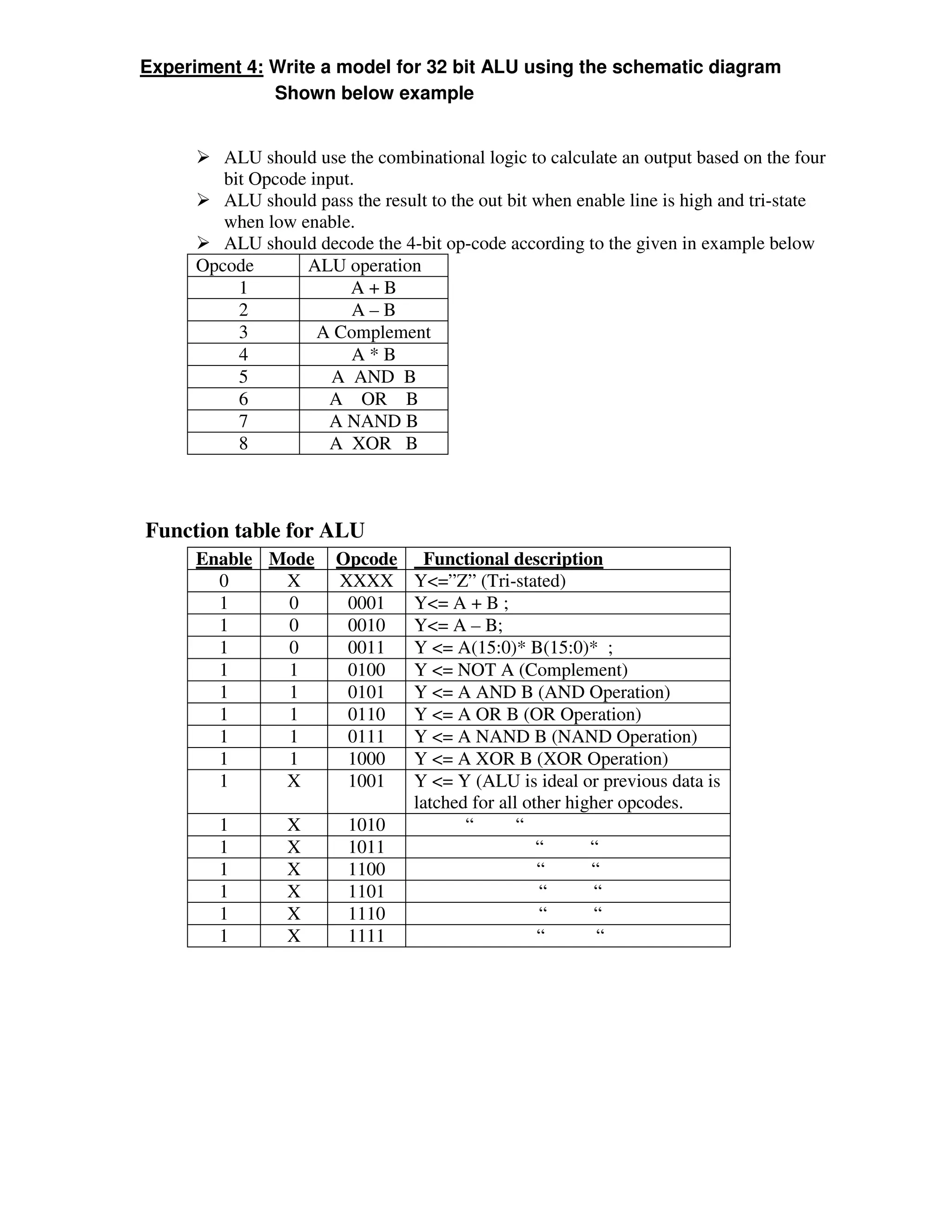
![ARTHAMETIC LOGIC UNIT (ALU)
ALU is logic circuit which is able to perform different arithmetic and logical
function basically ALU is the heart of central processing unit (CPU).
Cin Cin + 1 (CY)
Data One stage of
i/p 32 Arithmetic
A 32 circuit
B
4 0 32
Opcode [3:0] 0
2:1
Enabl 32 Mux
32 Y
Control
e 1
Signals 1 (Data o/p)
One stage of
Logic circuit
Mode
Mode : ‘0’____ Arthmatic operation
‘1’____Logic operation
Enable ‘0’ Y <= “ Z “
‘1’ Out put performed
Note: For A*B, A&B lower 16 bit [15:0] can be taken in to consideration.](https://image.slidesharecdn.com/experiment-write-vhdl-code-for-realize-all-logic-gates-111020142801-phpapp01/75/Experiment-write-vhdl-code-for-realize-all-logic-gates-31-2048.jpg)


![ARTHAMETIC LOGIC UNIT (ALU)
ALU is logic circuit which is able to perform different arithmetic and logical
function basically ALU is the heart of central processing unit (CPU).
Cin Cin + 1 (CY)
Data One stage of
i/p 32 Arithmetic
A 32 circuit
B
4 0 32
Opcode [3:0] 0
2:1
Enabl 32 Mux
32 Y
Control
e 1
Signals 1 (Data o/p)
One stage of
Logic circuit
Mode
Mode : ‘0’____ Arthmatic operation
‘1’____Logic operation
Enable ‘0’ Y <= “ Z “
‘1’ Out put performed
Note: For A*B, A&B lower 16 bit [15:0] can be taken in to consideration.](https://crownmelresort.com/image.slidesharecdn.com/experiment-write-vhdl-code-for-realize-all-logic-gates-111020142801-phpapp01/75/Experiment-write-vhdl-code-for-realize-all-logic-gates-31-2048.jpg)