Downloaded 10 times
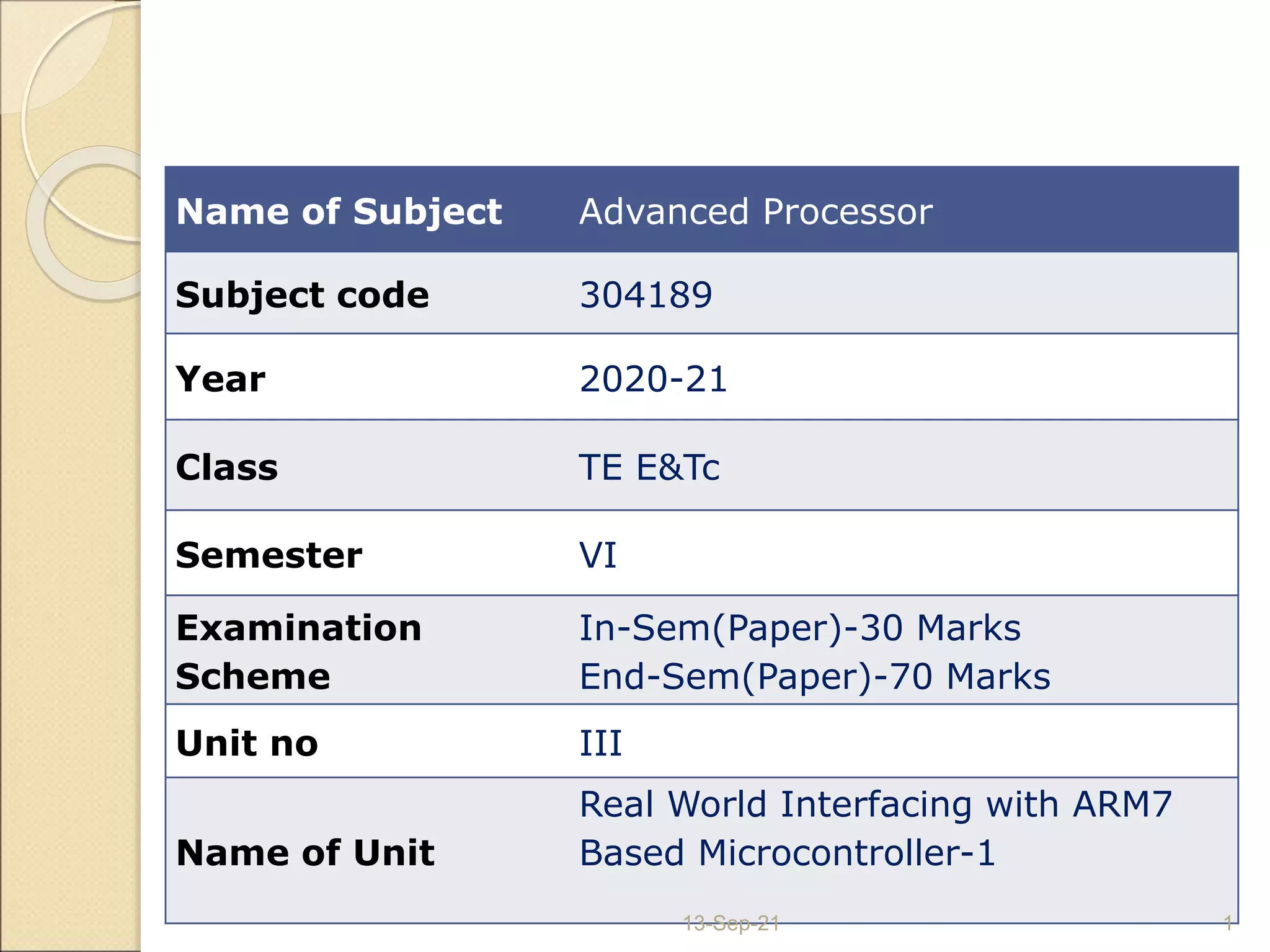

![U0DLL and U0DLM (UART0 Divisor Latch
Registers)
Both of them hold 8-bit values.
These register together form a 16 bit divisor value
which is used in baud rate generation.
U0DLM holds the upper 8 bits and U0DLL holds the
lower 8 bits and the formation is “[U0DLM:U0DLL].
Since these form a divisor value and division by zero
is invalid,the starting for U0DLL is 0x01(not 0x00)i.e
starting value in combined formation is[0x00:0x01]
i.e.0x0001.
In order to access and use these registers
properly,DLAB bit in U0LCR must be set to 1.
13-Sep-21 14](https://image.slidesharecdn.com/apuart-210913175734/75/UART-14-2048.jpg)


![U0DLL and U0DLM (UART0 Divisor Latch
Registers)
Both of them hold 8-bit values.
These register together form a 16 bit divisor value
which is used in baud rate generation.
U0DLM holds the upper 8 bits and U0DLL holds the
lower 8 bits and the formation is “[U0DLM:U0DLL].
Since these form a divisor value and division by zero
is invalid,the starting for U0DLL is 0x01(not 0x00)i.e
starting value in combined formation is[0x00:0x01]
i.e.0x0001.
In order to access and use these registers
properly,DLAB bit in U0LCR must be set to 1.
13-Sep-21 14](https://crownmelresort.com/image.slidesharecdn.com/apuart-210913175734/75/UART-14-2048.jpg)


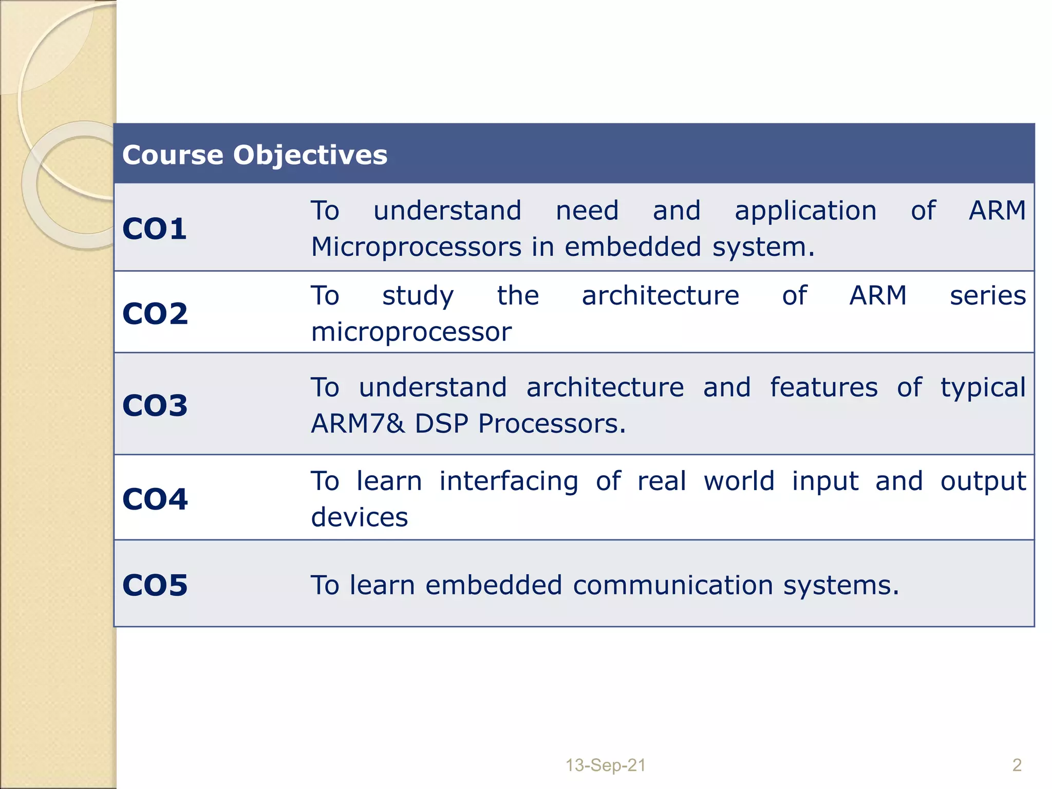
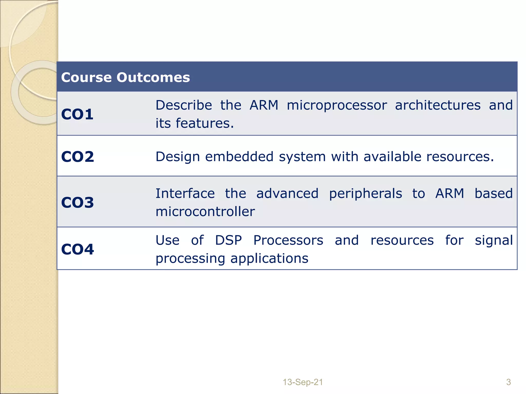
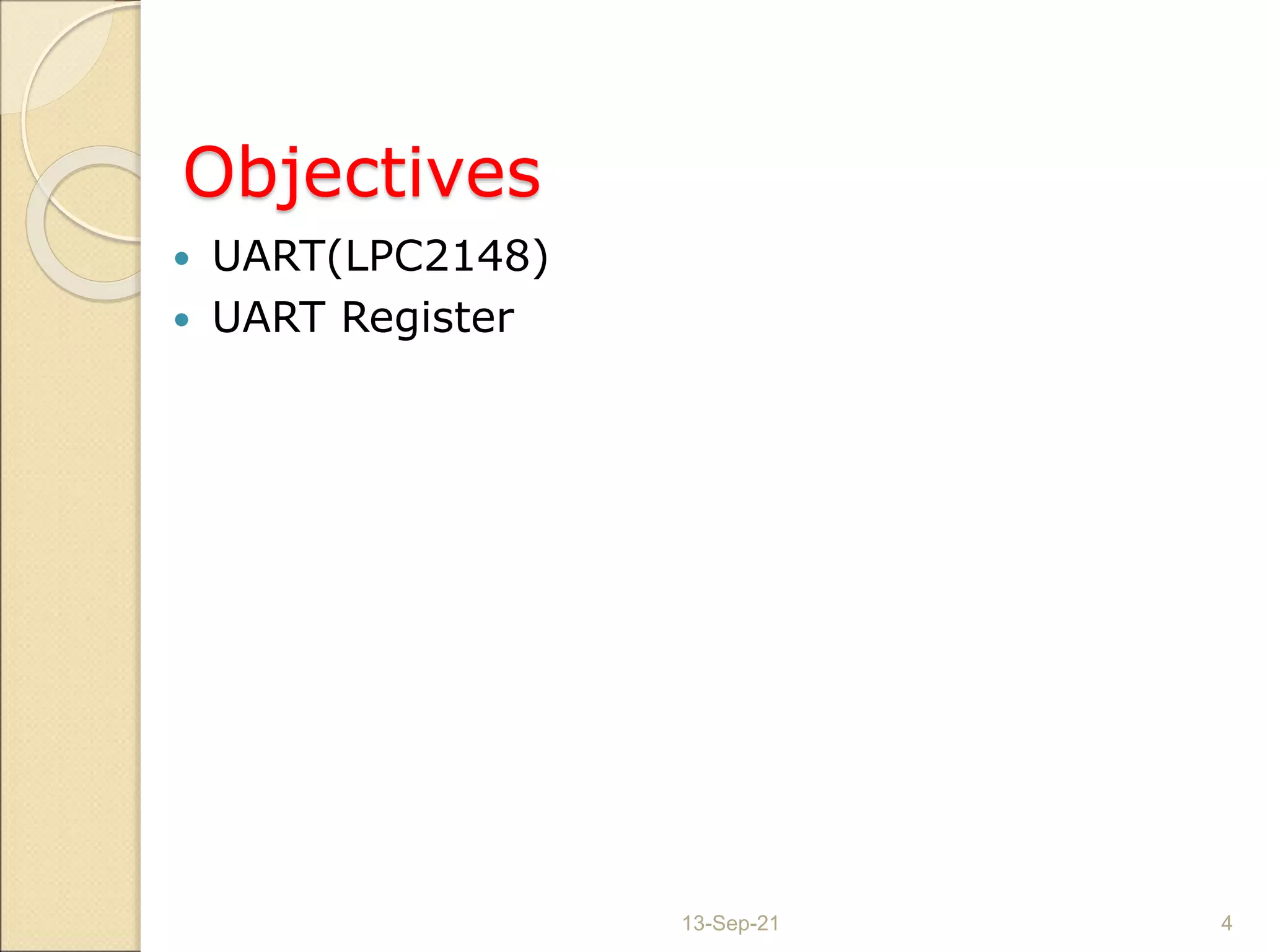
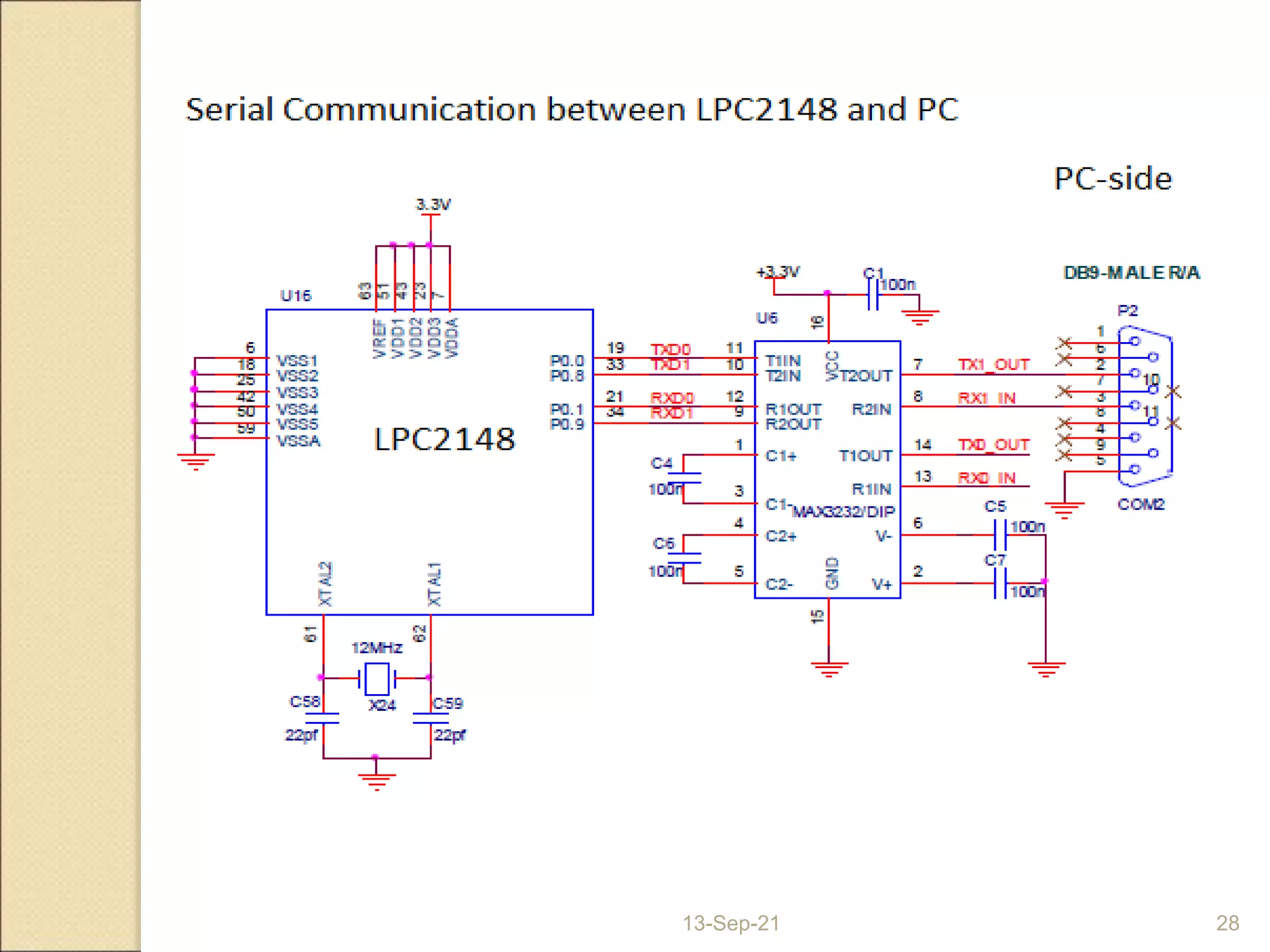
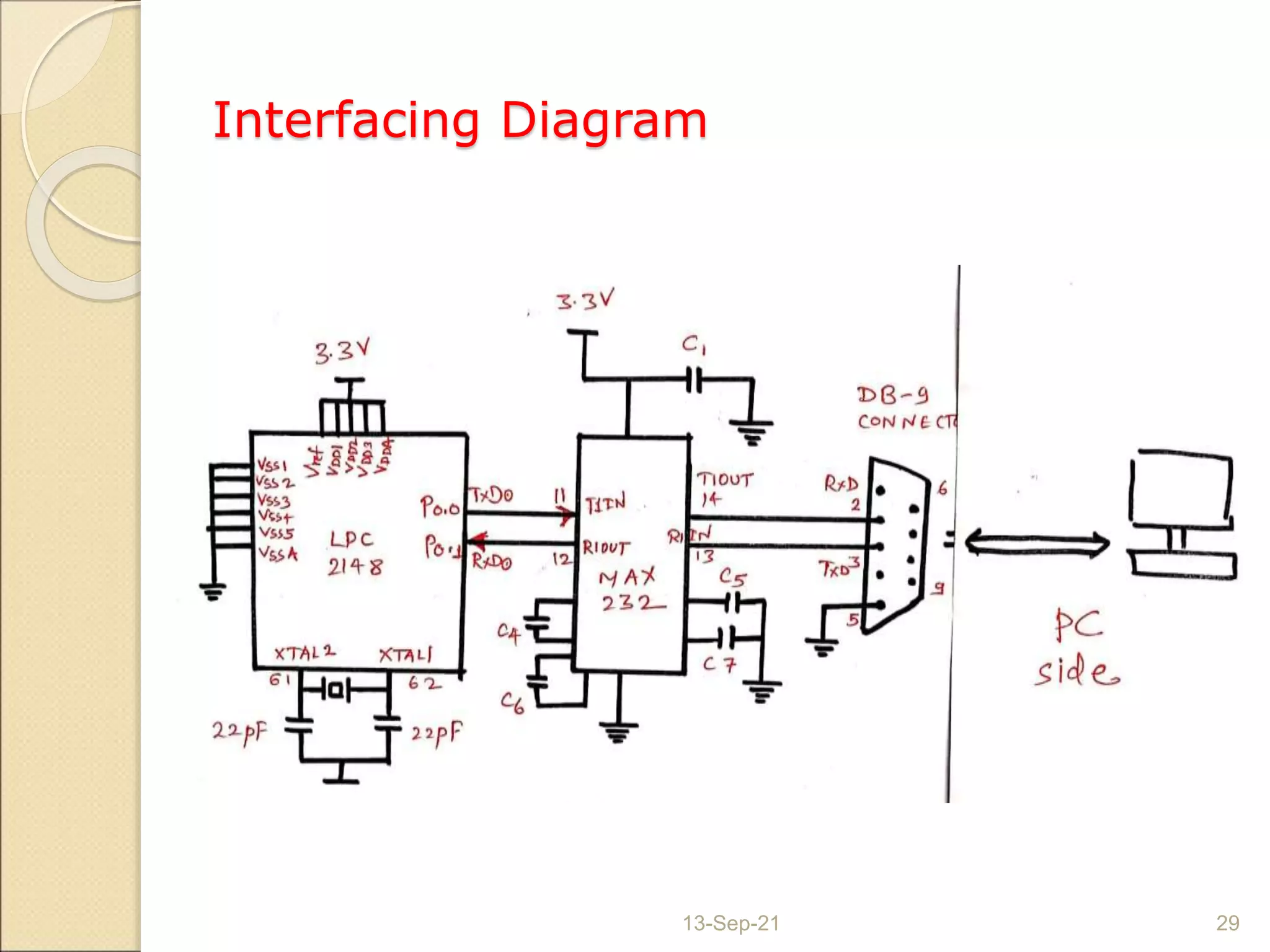
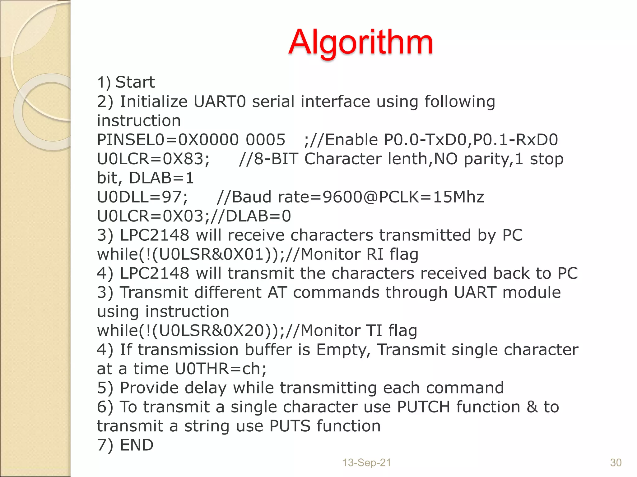
This document provides information about interfacing an ARM7 microcontroller with a UART module. It begins with course objectives and outcomes related to real-world interfacing. It then describes the basic operation and frame structure of UART serial communication. Details are given about the UART module and registers on the LPC2148 microcontroller, including how to configure pins for UART functionality and set the baud rate. An algorithm is provided to transmit and receive data through the UART using various register commands.


![ANPARA THERMAL POWER STATION[1] sangam.pdf](https://cdn.slidesharecdn.com/ss_thumbnails/anparathermalpowerstation1sangam-251121115219-9261cde4-thumbnail.jpg?width=640&height=640&fit=bounds)


