Download to read offline
![Kaleeswari .S, Saranya .K, Muniraj N. J. R, International Journal of Advance Research, Ideas and Innovations in
Technology.
© 2017, www.IJARIIT.com All Rights Reserved Page | 115
ISSN: 2454-132X
Impact factor: 4.295
(Volume3, Issue6)
Available online at www.ijariit.com
Efficient Implementation of Full Adder for Power Analysis in
CMOS Technology
S. Kaleeswari
Assistant Professor,
Department of ECE,
Tejaa Shakthi Institute of Technology for
Women, Coimbatore, Tamil Nadu
saranyaautomatic@gmail.com
K. Saranya
PG Scholar
Department of ECE,
Tejaa Shakthi Institute of Technology for
Women, Coimbatore, Tamil Nadu
skaviya18@gmail.com
Dr. N. J. R Muniraj
Principal
Department of ECE,
Tejaa Shakthi Institute of Technology for
Women, Coimbatore, Tamil Nadu
njrmuniraj@yahoo.co.in
Abstract: In recent days, the real-time application and fast arithmetic operations require highly efficient arithmetic hardware
architecture to improve the system performances. The adder plays a vital role in digital circuits, the earlier hardware
architecture using conventional CMOS and transmission logic gate based full adder design. Moreover, the techniques using
more number of transistors and consume larger power and delay so we proposed the techniques pass-transistor logic and
transmission gate based hybrid pass logic. The hybrid technique is used to reduce the number of the transistor, so the delay
and power consumption will be reduced when compared with the earlier techniques. The proposed technique design was
implemented using 16 transistors in 180nm CMOS technology and it consumes 8.2075nW power and the delay reduced to
5.0146ns.
Keyword: CMOS. Transmission gate, Pass-Transistor Logic, Adder.
I. INTRODUCTION
A full adder is one of the most fundamental building blocks of all the circuit application. Standard static CMOS, dynamic
CMOS logic, complementary pass transistor logic (CPL) and transmission gate full adder are the most logic styles in the
conventional domain [1]. In general, one bit full adder core has three inputs (A, B and carry in Ci) and two outputs (sum S and
carry out Co).The adder performance may improve the power and speed with driving capability. The performance of full adder
can significantly affect the system performance [2]. At the circuit level, the optimized design is used to avoid degradation in the
output voltage, and it consumes less power and delay in the critical path [5]. Using the complementary pass transistor logic (CPL)
the adder circuit will operate at low supply voltage with signal integrity [6]. From the gate logic design, the full adder can be
implemented using exclusive-OR gates, since the sum can be expressed as an XOR function and output can be expressed as a
multiplexer function [7].
The power dissipation characteristics are compared qualitatively and quantitatively with gate implementation. Lowering
supply voltage also increases the circuit delay and degrades the drivability of the cells [8]. Clustered voltage scaling (CVS) and
Dual voltage supply (dual-VS) have been proposed to maintain the chip throughput by selectively lowering the supply voltage.The
critical path traverses from the carry-in to the carry-out of the full adders. To optimize and analyze the performance of different
full adders, a tree-structured setup is proposed. Each of these modules is implemented, optimized and tested separately [6].
Several full-adder cells are composed by connecting these modules. Adders are an extensively used component in data paths and
the design and analysis are required for these units to obtain optimum performance.
To execute an arithmetic operation a circuit can consume very low power by clocking at low frequency to complete the
operation.GDI techniques are used to reduce power consumption, propagation delay [9]-[14]. The major sources of power
consumption in CMOS circuits are switching power, short circuit power and leakage power [15]. The performance and
complexity at the transistor level directly influence the overall performance of the system. The gate-based Full adders with
conventional methods result in a higher number of transistors and consequently more power consumption, delay, and area wastage
[17] –[19]. Lowering the supply voltage appears to reduce power consumption. However, lowering supply voltage also increases
circuit delay and degrades the drivability of cells designed with certain logic styles [20]-[23]. The power-delay product (PDP)
represents a tradeoff to be optimized between two conflicting criteria of power dissipation and circuit latency. In VLSI the adders
are basic components for an ALU. There is N number of adders their own advantage and disadvantages.](https://image.slidesharecdn.com/efficientimplementationoffulladderforpoweranalysisincmostechnology-180109055319/75/Efficient-implementation-of-full-adder-for-power-analysis-in-cmos-technology-1-2048.jpg)
![Kaleeswari .S, Saranya .K, Muniraj N. J. R, International Journal of Advance Research, Ideas and Innovations in
Technology.
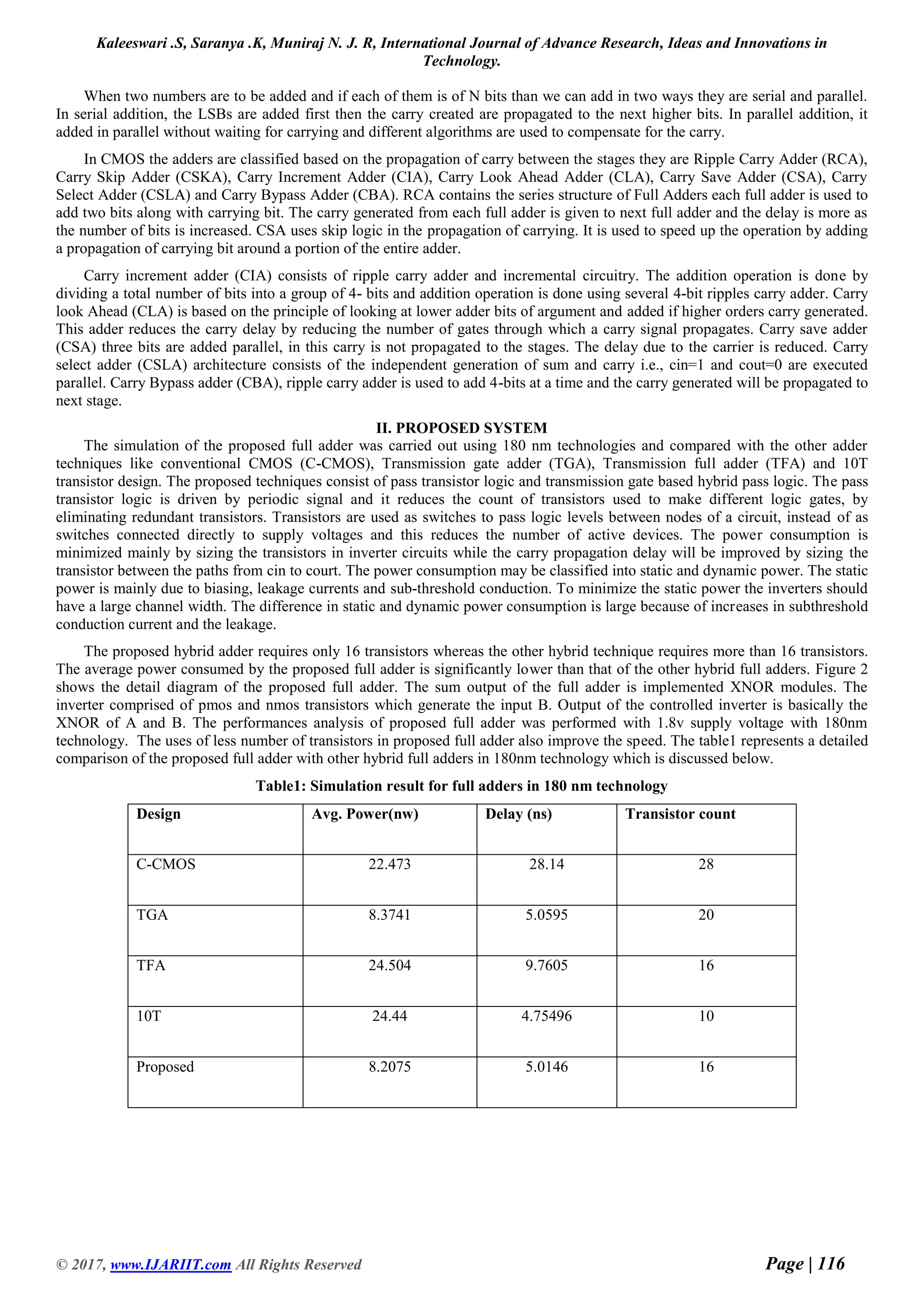
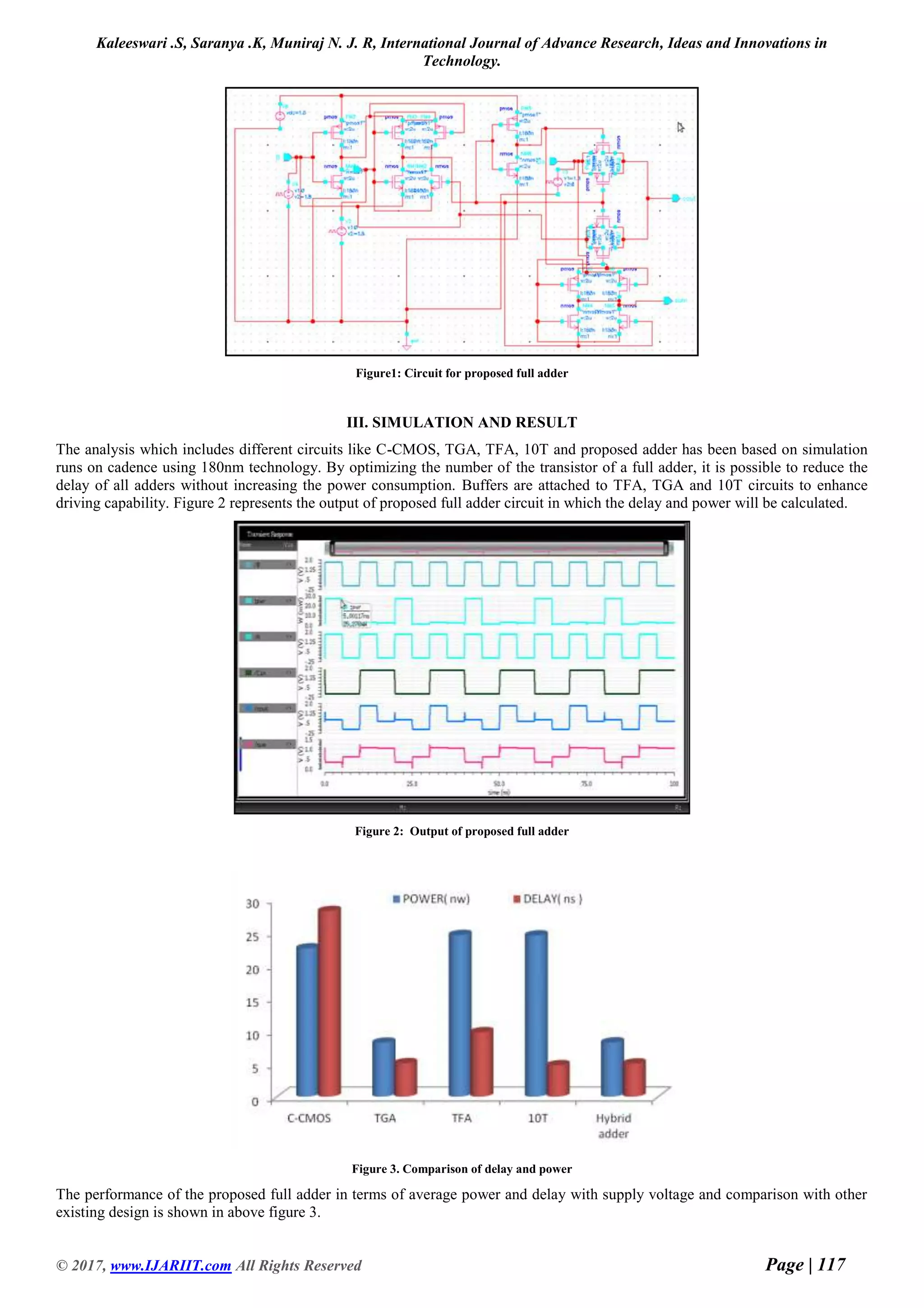
© 2017, www.IJARIIT.com All Rights Reserved Page | 118
CONCLUSION
In this paper, we proposed a low power hybrid 1-bit full adder in CMOS design. The simulation was carried out using cadence
virtuoso tool 180 nm technologies and compared with other designs like C-CMOS, TFA, TGA, and 10T. The simulation result
offered that the established proposed adder reduces the power compared with earlier designs. The hybrid technique is used to
reduce the no of the transistor, so the delay and power consumption will be reduced when compared with the earlier techniques.
The proposed technique design was implemented using 16 transistors in 180nm CMOS technology and it consumes 8.2075nW
power and the delay reduced to 5.0146ns.
REFERENCES
[1] C.K.Tung, Y. C. Hung, S. H. Shieh and G. S. Huang, (2007), ‘‘A low-power high-speed hybrid CMOS full adder for
embedded system’’, in proc. IEEE conf. Design diagnosis electron circuits syst., vol.13, pp.1-4.
[2] S. Goel, A. Kumar and M. A. Bayoumi, (2006), ‘‘Design of robust, energy-efficient full adders for deep-sub micrometer
design using hybrid-CMOS logic style’’, IEEE trans. very large scale integer. (VLSI) syst., vol.14, no.12, pp. 1309-1312.
[3] D. Radhakrishnan, (2001), ‘‘Low-voltage low-power CMOS full adder’’, IEEE proc. circuit device syst., vol.148, n0.1, pp.
19-24.
[4] R. Zimmermann and W. Fichtner, (1997) ‘‘Low-power logic styles: CMOS versus pass-transistor logic’’, IEEE J .Solid-state
circuits, vol.32, no.7, pp. 1079-1997.
[5] C. H. Chang, J.M.Gu and M. Zhang, (2005), ‘‘A review of 0.18 µm full adder performances for tree structured arithmetic
circuits’’, IEEE trans. Very large scale integer. (VLSI) syst., vol. 13, no. 6, pp. 686-695.
[6] A. M. Sharms, T. K. Darwish, and M. A. Bayoumi, (2002), ‘‘Performance analysis of low-power 1-bit CMOS full adder
cells’’, IEEE trans. Very large scale integer. (VLSI) syst., vol.10, no.1, pp. 20-29.
[7] M. Zhang, J. Gu and C. H. Chang, (2003), ‘‘A novel hybrid pass logic with static CMOS output drive full-adder cell’’, in
proc. Int.symp.circuits syst., pp. 317-320.
[8] S. Wariya, G. Singh, R. K. Nagaraj, and S. Tiwari, (2011)’ ‘‘Design analysis of XOR (4T) based low voltage CMOS full adder
circuit’’, in proc.IEEE Nirma Univ. Int. conf.Eng. (NUiCONE), PP. 1-7.
[9] S. Goel, M. Elgamel, and M. A. Bayoumi, (2003), ‘‘Novel design methodology for high-performance XOR-XNOR circuit
design’’, in proc. 16th
symp.integr.circuits system.design (SBCCI), pp. 71-76.
[10] J.M.Wang, S.C.Fang and W.S.Feng, (1994), ‘‘New efficient designs for XOR and XNOR functions on the transistor level’’,
IEEE.J. Solid-state Circuits, vol. 29, no.7, pp. 780-786.
[11] M. J. Zavarei, M. R. Baghbanmanesh, E. Kargaran, H. Nabovati and A. Golmakani, (2011), ‘‘Design of new full adder using
hybrid-CMOS logic style’’, in proc. 18th
IEEE Int. conf. Electron.circuit system. (ICECS), PP. 451-454.
[12] M.Alioto, G.Dicataldo and G.Palumbo, (2007), ‘‘Mixed full adder topologies for high-performance low-power arithmetic
circuits’’, microelectronics. J., vol. 38, no. 1, pp. 130-139.
[13] X. Wu and F.Prosser, (1998), ‘‘Design of ternary CMOS circuits based on transmission function theory’’, Int. J.Electron.,
vol. 65, no. 5, pp. 891-905.
[14] K. Navi, M. H. Moaiyeri, R. F. Mizaee, O. Hashemipour and B. M. Nezhad, (2009), ‘‘Two new low-power full adders based
on majority-not gates’’, microelectron.J, vol. 40, no. 1, pp. 126-130.
[15] H.T. Bui, Y.Wang and Y.Jiang, (2002), ‘‘Design and analysis of low-power 10-transistor full adders using novel XOR-
XNOR gates’’, IEEE Trans.circuits system.II Analog digit signal process., vol. 49, no. 1, pp. 25-30.
[16] K. Navi, (2009), ‘‘A novel low-power full adder cell with a new technique in designing logical gates based on static CMOS
inverter’’, microelectron.J, vol. 40, no. 10, pp. 1441-1448.
[17] S. Kaleeswari is presently pursuing Master degree in VLSI Design at Tejaa Shakthi Institute of Technology, Coimbatore.
She is interested in CMOS VLSI design using Cadence Virtuoso.
[18] K. Saranya obtains BE ECE in Avinashilingam Deemed university and ME VLSI design in Anna university Coimbatore and
she is presently working as a Assistant professor in Department of ECE at Tejaa Shakthi institute of Technology,
Coimbatore and 6 years guiding students.](https://image.slidesharecdn.com/efficientimplementationoffulladderforpoweranalysisincmostechnology-180109055319/75/Efficient-implementation-of-full-adder-for-power-analysis-in-cmos-technology-4-2048.jpg)
![Kaleeswari .S, Saranya .K, Muniraj N. J. R, International Journal of Advance Research, Ideas and Innovations in
Technology.
© 2017, www.IJARIIT.com All Rights Reserved Page | 115
ISSN: 2454-132X
Impact factor: 4.295
(Volume3, Issue6)
Available online at www.ijariit.com
Efficient Implementation of Full Adder for Power Analysis in
CMOS Technology
S. Kaleeswari
Assistant Professor,
Department of ECE,
Tejaa Shakthi Institute of Technology for
Women, Coimbatore, Tamil Nadu
saranyaautomatic@gmail.com
K. Saranya
PG Scholar
Department of ECE,
Tejaa Shakthi Institute of Technology for
Women, Coimbatore, Tamil Nadu
skaviya18@gmail.com
Dr. N. J. R Muniraj
Principal
Department of ECE,
Tejaa Shakthi Institute of Technology for
Women, Coimbatore, Tamil Nadu
njrmuniraj@yahoo.co.in
Abstract: In recent days, the real-time application and fast arithmetic operations require highly efficient arithmetic hardware
architecture to improve the system performances. The adder plays a vital role in digital circuits, the earlier hardware
architecture using conventional CMOS and transmission logic gate based full adder design. Moreover, the techniques using
more number of transistors and consume larger power and delay so we proposed the techniques pass-transistor logic and
transmission gate based hybrid pass logic. The hybrid technique is used to reduce the number of the transistor, so the delay
and power consumption will be reduced when compared with the earlier techniques. The proposed technique design was
implemented using 16 transistors in 180nm CMOS technology and it consumes 8.2075nW power and the delay reduced to
5.0146ns.
Keyword: CMOS. Transmission gate, Pass-Transistor Logic, Adder.
I. INTRODUCTION
A full adder is one of the most fundamental building blocks of all the circuit application. Standard static CMOS, dynamic
CMOS logic, complementary pass transistor logic (CPL) and transmission gate full adder are the most logic styles in the
conventional domain [1]. In general, one bit full adder core has three inputs (A, B and carry in Ci) and two outputs (sum S and
carry out Co).The adder performance may improve the power and speed with driving capability. The performance of full adder
can significantly affect the system performance [2]. At the circuit level, the optimized design is used to avoid degradation in the
output voltage, and it consumes less power and delay in the critical path [5]. Using the complementary pass transistor logic (CPL)
the adder circuit will operate at low supply voltage with signal integrity [6]. From the gate logic design, the full adder can be
implemented using exclusive-OR gates, since the sum can be expressed as an XOR function and output can be expressed as a
multiplexer function [7].
The power dissipation characteristics are compared qualitatively and quantitatively with gate implementation. Lowering
supply voltage also increases the circuit delay and degrades the drivability of the cells [8]. Clustered voltage scaling (CVS) and
Dual voltage supply (dual-VS) have been proposed to maintain the chip throughput by selectively lowering the supply voltage.The
critical path traverses from the carry-in to the carry-out of the full adders. To optimize and analyze the performance of different
full adders, a tree-structured setup is proposed. Each of these modules is implemented, optimized and tested separately [6].
Several full-adder cells are composed by connecting these modules. Adders are an extensively used component in data paths and
the design and analysis are required for these units to obtain optimum performance.
To execute an arithmetic operation a circuit can consume very low power by clocking at low frequency to complete the
operation.GDI techniques are used to reduce power consumption, propagation delay [9]-[14]. The major sources of power
consumption in CMOS circuits are switching power, short circuit power and leakage power [15]. The performance and
complexity at the transistor level directly influence the overall performance of the system. The gate-based Full adders with
conventional methods result in a higher number of transistors and consequently more power consumption, delay, and area wastage
[17] –[19]. Lowering the supply voltage appears to reduce power consumption. However, lowering supply voltage also increases
circuit delay and degrades the drivability of cells designed with certain logic styles [20]-[23]. The power-delay product (PDP)
represents a tradeoff to be optimized between two conflicting criteria of power dissipation and circuit latency. In VLSI the adders
are basic components for an ALU. There is N number of adders their own advantage and disadvantages.](https://crownmelresort.com/image.slidesharecdn.com/efficientimplementationoffulladderforpoweranalysisincmostechnology-180109055319/75/Efficient-implementation-of-full-adder-for-power-analysis-in-cmos-technology-1-2048.jpg)


![Kaleeswari .S, Saranya .K, Muniraj N. J. R, International Journal of Advance Research, Ideas and Innovations in
Technology.
© 2017, www.IJARIIT.com All Rights Reserved Page | 118
CONCLUSION
In this paper, we proposed a low power hybrid 1-bit full adder in CMOS design. The simulation was carried out using cadence
virtuoso tool 180 nm technologies and compared with other designs like C-CMOS, TFA, TGA, and 10T. The simulation result
offered that the established proposed adder reduces the power compared with earlier designs. The hybrid technique is used to
reduce the no of the transistor, so the delay and power consumption will be reduced when compared with the earlier techniques.
The proposed technique design was implemented using 16 transistors in 180nm CMOS technology and it consumes 8.2075nW
power and the delay reduced to 5.0146ns.
REFERENCES
[1] C.K.Tung, Y. C. Hung, S. H. Shieh and G. S. Huang, (2007), ‘‘A low-power high-speed hybrid CMOS full adder for
embedded system’’, in proc. IEEE conf. Design diagnosis electron circuits syst., vol.13, pp.1-4.
[2] S. Goel, A. Kumar and M. A. Bayoumi, (2006), ‘‘Design of robust, energy-efficient full adders for deep-sub micrometer
design using hybrid-CMOS logic style’’, IEEE trans. very large scale integer. (VLSI) syst., vol.14, no.12, pp. 1309-1312.
[3] D. Radhakrishnan, (2001), ‘‘Low-voltage low-power CMOS full adder’’, IEEE proc. circuit device syst., vol.148, n0.1, pp.
19-24.
[4] R. Zimmermann and W. Fichtner, (1997) ‘‘Low-power logic styles: CMOS versus pass-transistor logic’’, IEEE J .Solid-state
circuits, vol.32, no.7, pp. 1079-1997.
[5] C. H. Chang, J.M.Gu and M. Zhang, (2005), ‘‘A review of 0.18 µm full adder performances for tree structured arithmetic
circuits’’, IEEE trans. Very large scale integer. (VLSI) syst., vol. 13, no. 6, pp. 686-695.
[6] A. M. Sharms, T. K. Darwish, and M. A. Bayoumi, (2002), ‘‘Performance analysis of low-power 1-bit CMOS full adder
cells’’, IEEE trans. Very large scale integer. (VLSI) syst., vol.10, no.1, pp. 20-29.
[7] M. Zhang, J. Gu and C. H. Chang, (2003), ‘‘A novel hybrid pass logic with static CMOS output drive full-adder cell’’, in
proc. Int.symp.circuits syst., pp. 317-320.
[8] S. Wariya, G. Singh, R. K. Nagaraj, and S. Tiwari, (2011)’ ‘‘Design analysis of XOR (4T) based low voltage CMOS full adder
circuit’’, in proc.IEEE Nirma Univ. Int. conf.Eng. (NUiCONE), PP. 1-7.
[9] S. Goel, M. Elgamel, and M. A. Bayoumi, (2003), ‘‘Novel design methodology for high-performance XOR-XNOR circuit
design’’, in proc. 16th
symp.integr.circuits system.design (SBCCI), pp. 71-76.
[10] J.M.Wang, S.C.Fang and W.S.Feng, (1994), ‘‘New efficient designs for XOR and XNOR functions on the transistor level’’,
IEEE.J. Solid-state Circuits, vol. 29, no.7, pp. 780-786.
[11] M. J. Zavarei, M. R. Baghbanmanesh, E. Kargaran, H. Nabovati and A. Golmakani, (2011), ‘‘Design of new full adder using
hybrid-CMOS logic style’’, in proc. 18th
IEEE Int. conf. Electron.circuit system. (ICECS), PP. 451-454.
[12] M.Alioto, G.Dicataldo and G.Palumbo, (2007), ‘‘Mixed full adder topologies for high-performance low-power arithmetic
circuits’’, microelectronics. J., vol. 38, no. 1, pp. 130-139.
[13] X. Wu and F.Prosser, (1998), ‘‘Design of ternary CMOS circuits based on transmission function theory’’, Int. J.Electron.,
vol. 65, no. 5, pp. 891-905.
[14] K. Navi, M. H. Moaiyeri, R. F. Mizaee, O. Hashemipour and B. M. Nezhad, (2009), ‘‘Two new low-power full adders based
on majority-not gates’’, microelectron.J, vol. 40, no. 1, pp. 126-130.
[15] H.T. Bui, Y.Wang and Y.Jiang, (2002), ‘‘Design and analysis of low-power 10-transistor full adders using novel XOR-
XNOR gates’’, IEEE Trans.circuits system.II Analog digit signal process., vol. 49, no. 1, pp. 25-30.
[16] K. Navi, (2009), ‘‘A novel low-power full adder cell with a new technique in designing logical gates based on static CMOS
inverter’’, microelectron.J, vol. 40, no. 10, pp. 1441-1448.
[17] S. Kaleeswari is presently pursuing Master degree in VLSI Design at Tejaa Shakthi Institute of Technology, Coimbatore.
She is interested in CMOS VLSI design using Cadence Virtuoso.
[18] K. Saranya obtains BE ECE in Avinashilingam Deemed university and ME VLSI design in Anna university Coimbatore and
she is presently working as a Assistant professor in Department of ECE at Tejaa Shakthi institute of Technology,
Coimbatore and 6 years guiding students.](https://crownmelresort.com/image.slidesharecdn.com/efficientimplementationoffulladderforpoweranalysisincmostechnology-180109055319/75/Efficient-implementation-of-full-adder-for-power-analysis-in-cmos-technology-4-2048.jpg)

The document presents a study on an efficient implementation of a full adder using CMOS technology, specifically a hybrid design using pass-transistor logic and transmission gate techniques. The proposed full adder, utilizing 16 transistors, shows significant improvements in power consumption (8.2075nW) and delay (5.0146ns) compared to conventional designs. The results demonstrate that the hybrid approach effectively reduces both transistor count and power consumption, enhancing overall circuit performance.