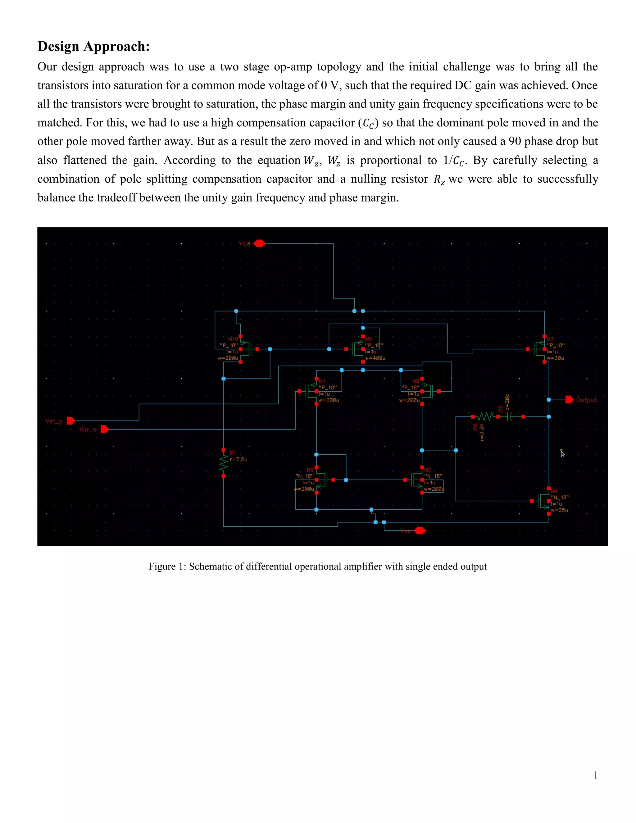
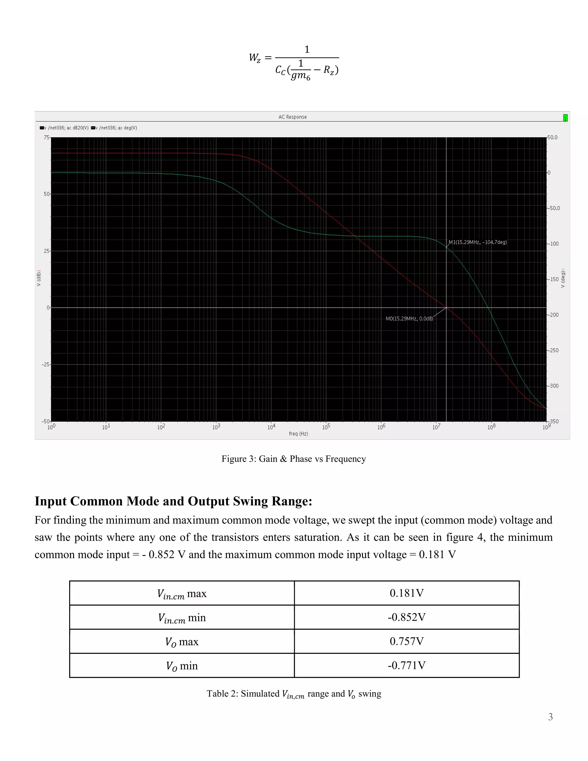
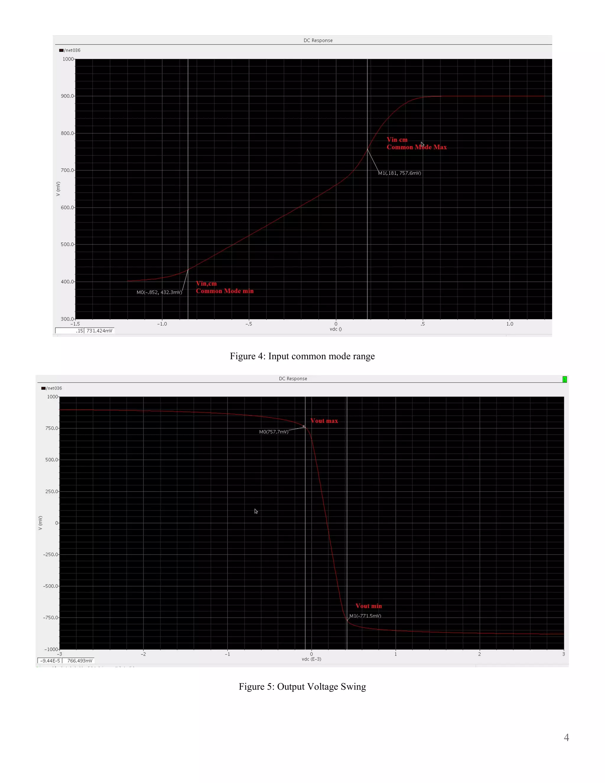
ECE 522
Project – Differential Input to Single Ended two Stage OP-AMP
by
Karthikvel Rathinavel
Chien-Chun, Yao
In partial fulfillment of the requirements for the course of
CMOS Integrated Circuits I
Department of Electrical Engineering and Computer Science
Oregon State University
Corvallis
December, 2015
1
Design Approach:
Our design approach was to use a two stage op-amp topology and the initial challenge was to bring all the
transistors into saturation for a common mode voltage of 0 V, such that the required DC gain was achieved. Once
all the transistors were brought to saturation, the phase margin and unity gain frequency specifications were to be
matched. For this, we had to use a high compensation capacitor ( ) so that the dominant pole moved in and the
other pole moved farther away. But as a result the zero moved in and which not only caused a 90 phase drop but
also flattened the gain. According to the equation , is proportional to 1/ . By carefully selecting a
combination of pole splitting compensation capacitor and a nulling resistor we were able to successfully
balance the tradeoff between the unity gain frequency and phase margin.
Figure 1: Schematic of differential operational amplifier with single ended output
2
Simulated Results:
Figure 2: Test bench Setup
Parameters Required Specifications Simulated Specifications
Load Capacitor 5 pF 5 pF
Power Supply 0.9 , 0.9 0.9 , 0.9
Open Loop Gain >= 60 dB 67.97 dB
Phase Margin >= 60° 75.3°
PUnity Gain Frequency >= 15 MHz 15.29 MHz
Table 1: Simulated Specifications vs Required Specifications
Gain and Phase Margin:
We applied and increased the value of so that higher unity gain frequency could be obtained. However, by
increasing we pushed the zero to lower frequency which decreased the phase margin. Therefore, a nulling
resistor, is introduced to eliminate the effect of the zero. Initially, the value of is kept close to 1/ and
the value of is set to 10pF. By introducing and , we got a better phase margin and unity gain frequency.
However, the initial requirement for PM and unity gain frequency is not met. Therefore, we increase to push
zero further away.
1
3
1
1
Figure 3: Gain & Phase vs Frequency
Input Common Mode and Output Swing Range:
For finding the minimum and maximum common mode voltage, we swept the input (common mode) voltage and
saw the points where any one of the transistors enters saturation. As it can be seen in figure 4, the minimum
common mode input = - 0.852 V and the maximum common mode input voltage = 0.181 V
. max 0.181V
. min -0.852V
max 0.757V
min -0.771V
Table 2: Simulated , range and swing
4
Figure 4: Input common mode range
Figure 5: Output Voltage Swing

Differntial Input to Single Ended Output, Two stage Op-amp

  • 1.
    ECE 522 Project –Differential Input to Single Ended two Stage OP-AMP by Karthikvel Rathinavel Chien-Chun, Yao In partial fulfillment of the requirements for the course of CMOS Integrated Circuits I Department of Electrical Engineering and Computer Science Oregon State University Corvallis December, 2015
  • 2.
    1 Design Approach: Our designapproach was to use a two stage op-amp topology and the initial challenge was to bring all the transistors into saturation for a common mode voltage of 0 V, such that the required DC gain was achieved. Once all the transistors were brought to saturation, the phase margin and unity gain frequency specifications were to be matched. For this, we had to use a high compensation capacitor ( ) so that the dominant pole moved in and the other pole moved farther away. But as a result the zero moved in and which not only caused a 90 phase drop but also flattened the gain. According to the equation , is proportional to 1/ . By carefully selecting a combination of pole splitting compensation capacitor and a nulling resistor we were able to successfully balance the tradeoff between the unity gain frequency and phase margin. Figure 1: Schematic of differential operational amplifier with single ended output
  • 3.
    2 Simulated Results: Figure 2:Test bench Setup Parameters Required Specifications Simulated Specifications Load Capacitor 5 pF 5 pF Power Supply 0.9 , 0.9 0.9 , 0.9 Open Loop Gain >= 60 dB 67.97 dB Phase Margin >= 60° 75.3° PUnity Gain Frequency >= 15 MHz 15.29 MHz Table 1: Simulated Specifications vs Required Specifications Gain and Phase Margin: We applied and increased the value of so that higher unity gain frequency could be obtained. However, by increasing we pushed the zero to lower frequency which decreased the phase margin. Therefore, a nulling resistor, is introduced to eliminate the effect of the zero. Initially, the value of is kept close to 1/ and the value of is set to 10pF. By introducing and , we got a better phase margin and unity gain frequency. However, the initial requirement for PM and unity gain frequency is not met. Therefore, we increase to push zero further away. 1
  • 4.
    3 1 1 Figure 3: Gain& Phase vs Frequency Input Common Mode and Output Swing Range: For finding the minimum and maximum common mode voltage, we swept the input (common mode) voltage and saw the points where any one of the transistors enters saturation. As it can be seen in figure 4, the minimum common mode input = - 0.852 V and the maximum common mode input voltage = 0.181 V . max 0.181V . min -0.852V max 0.757V min -0.771V Table 2: Simulated , range and swing
  • 5.
    4 Figure 4: Inputcommon mode range Figure 5: Output Voltage Swing