Download to read offline
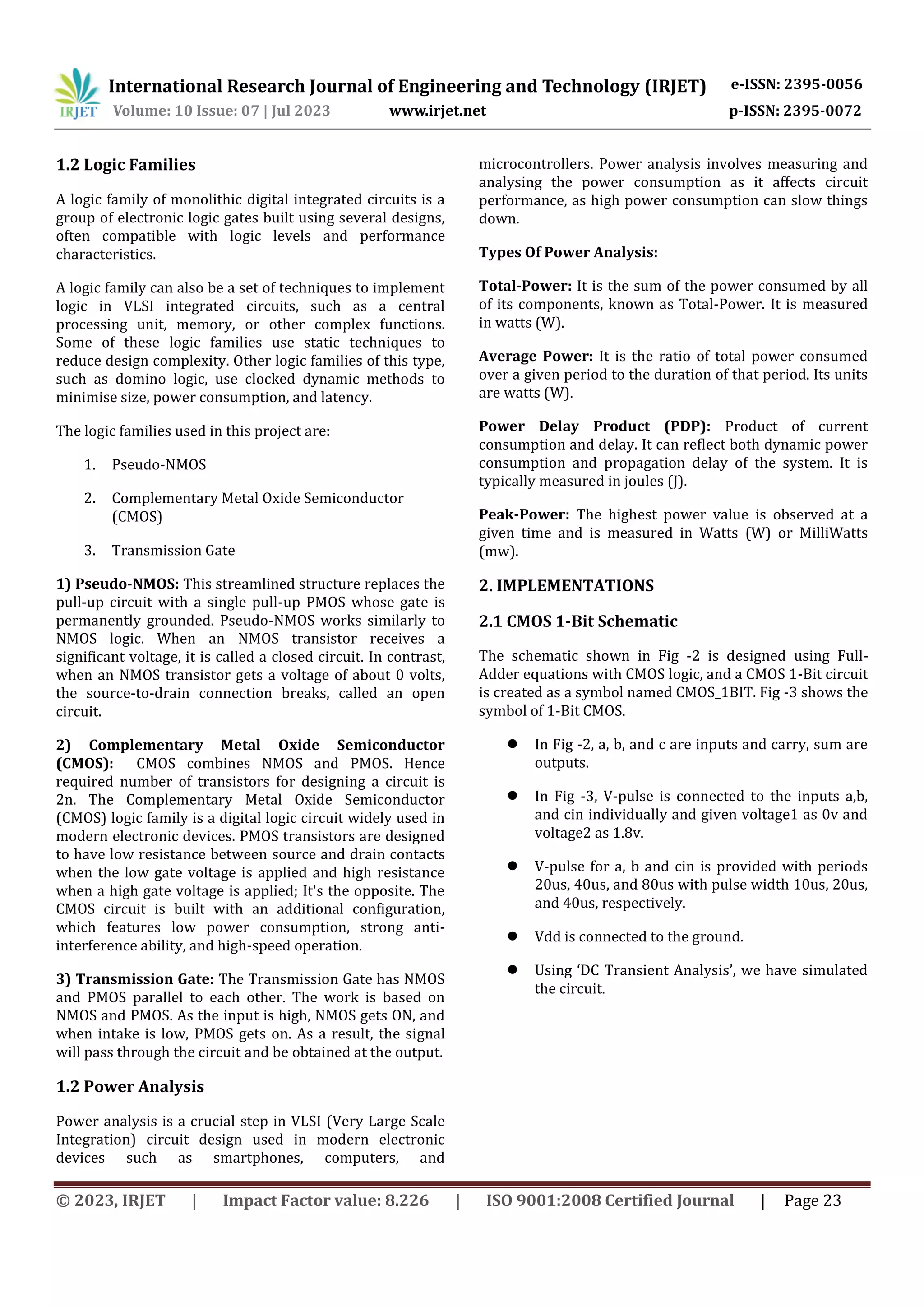
![International Research Journal of Engineering and Technology (IRJET) e-ISSN: 2395-0056
Volume: 10 Issue: 07 | Jul 2023 www.irjet.net p-ISSN: 2395-0072
© 2023, IRJET | Impact Factor value: 8.226 | ISO 9001:2008 Certified Journal | Page 27
Fig -18: Peak-Power value and Total-Power value of
Transmission Gate 64-Bit graph
3.2 Observations
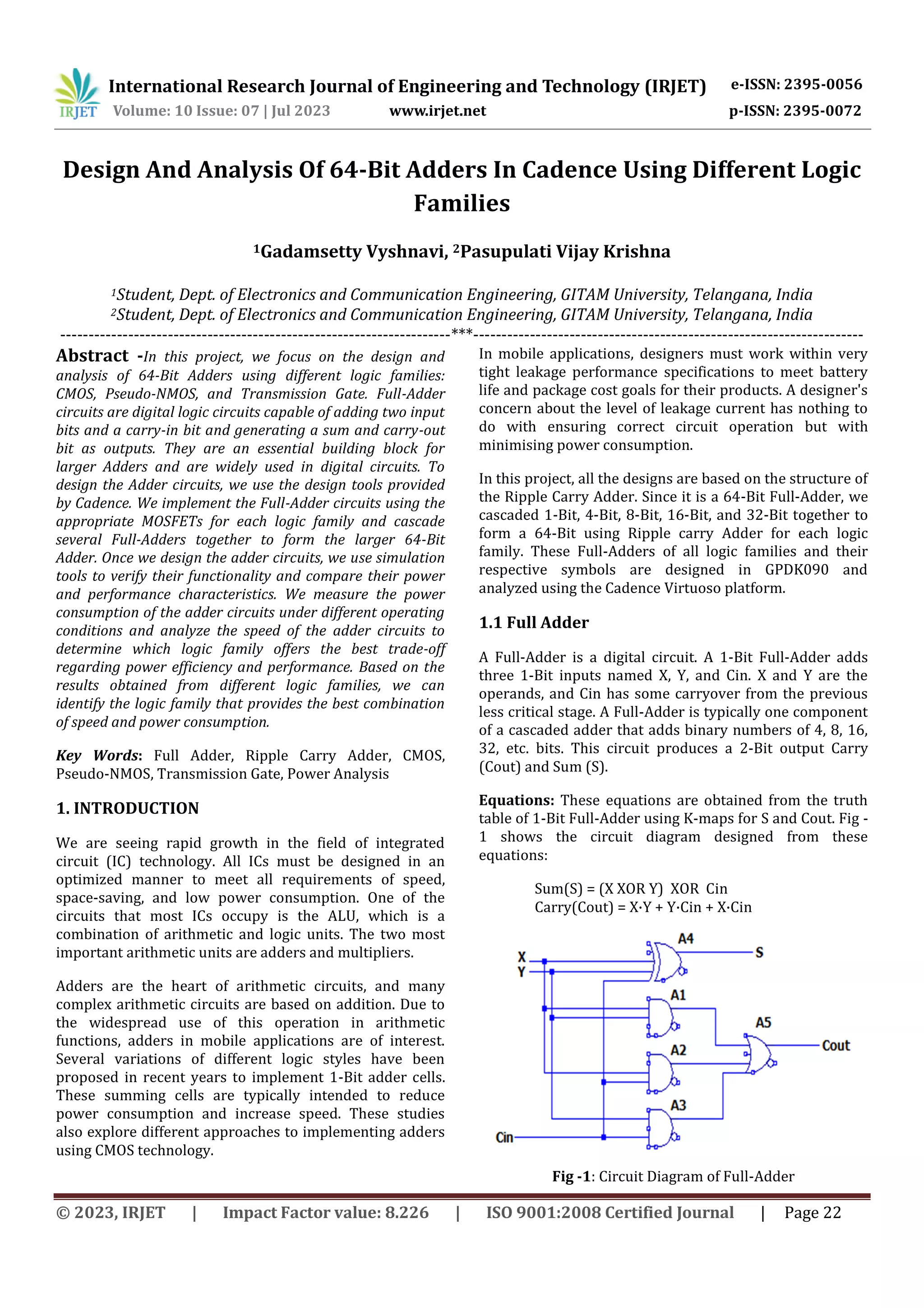
Table -1: Power Analysis Table
Logic Family CMOS
Transmissio
n Gate
Pseudo-
NMOS
No. of
Transistor (64-
Bit)
1792 1024 1152
Average Power
(W)
14.94E-3 219.0E-6 14.94E-3
Total-Power
(W)
23.77mW 46.34uW 23.77mW
Peak-Power (W) 23.28mW 4.17mW 23.49mW
Delay (s) 107.608n 275.903p 107.608n
Power Delay
Product (PDP)
(J)
1.607E-09 6.0422E-14 1.607E-09
Based on our design, the Table -1 shows that the CMOS
logic family has the highest transistor count among the
three options, while the Transmission Gate logic family
has the lowest. However, the Transmission Gate logic
family exhibits the highest peak power consumption,
while the Pseudo-NMOS and CMOS families have identical
power consumption characteristics. In terms of delay, all
three logic families have the same value of 107.608 ns. The
power-delay product (PDP) is the lowest for the
Transmission Gate logic family, indicating better efficiency
in terms of power consumption and performance.
However, it may vary to different applications. We can
choose the desired logic family based on cost, power, and
performance.
4. CONCLUSIONS
Firstly, Transmission Gate Full-Adder circuits use fewer
transistors than CMOS and pseudo-NMOS Full-Adder
circuits. Secondly, Transmission Gate Full-Adder circuits
also have lower delays than other logic families. Thirdly,
Transmission Gate Full-Adders exhibit better power delay
product results than CMOS and Pseudo-NMOS Full-Adder
circuits; however, the choice of the logic family to be used
ultimately depends on the application's specific
requirements, such as cost, power and performance.
Hence, from our designs, these conclusions highlight the
advantages of using Transmission Gate Full-Adder circuits
in specific applications where power consumption and
delay are critical factors.
REFERENCES
[1] Ren, Y., & Liu, Y. (2013). A novel approach to improve
the performance of asynchronous circuit design using
self-timed circuit. CiteSeerX, 10.1.1.676.9601.
[2] Jampani, Y., & Gupta, G. B. (2022, July).
Implementation of 1-Bit full adder circuit using pass
transistor logic. IJRASET International Journal for
Research in Applied Science & Engineering
Technology, 10(7), 4974-4981.
doi:10.22214/ijraset.2022.46097
[3] Trapti Mittal and Uma Sharma, “ANALYSIS OF FULL
ADDER FOR POWER EFFICIENT CIRCUIT DESIGN”,
IJARSE Vol. No. 4, Issue 10, October 2015
[4] Manjunath K M, Abdul Lateef Haroon P S, A. Pagi and
Ulaganathan J, "Analysis of various full-adder circuits
in cadence," 2015 International Conference on
Emerging Research in Electronics, Computer Science
and Technology (ICERECT), Mandya, India, 2015, pp.
90-97, doi: 10.1109/ERECT.2015.7498994.
[5] Bhati, Ankita and Rita Jain. “Low Power Delay -
Product CMOS Full Adder.” (2015).
[6] G. R. Padmini, O. Rajesh, K. Raghu, N. M. Sree, C.
Apurva and K. saikumar, "Design and Analysis of 8-bit
ripple Carry Adder using nine Transistor Full Adder,"
2021 7th International Conference on Advanced
Computing and Communication Systems (ICACCS),
Coimbatore, India, 2021, pp. 1982-1987, doi:
10.1109/ICACCS51430.2021.9441928.
[7] Zitong Han 2021 J. Phys.: Conf. Ser. 1754 012131
[8] Karunakaran, S., & Poonguzharselvi, B. (2017, March).
Exploration on power delay product of basic logic
gates for various CMOS logic styles. International
Journal of Engineering Studies, 9(2), 111-120.
doi:10.11648/j.ijes.20170902.12](https://image.slidesharecdn.com/irjet-v10i704-230815101719-b3fcba46/75/Design-And-Analysis-Of-64-Bit-Adders-In-Cadence-Using-Different-Logic-Families-6-2048.jpg)


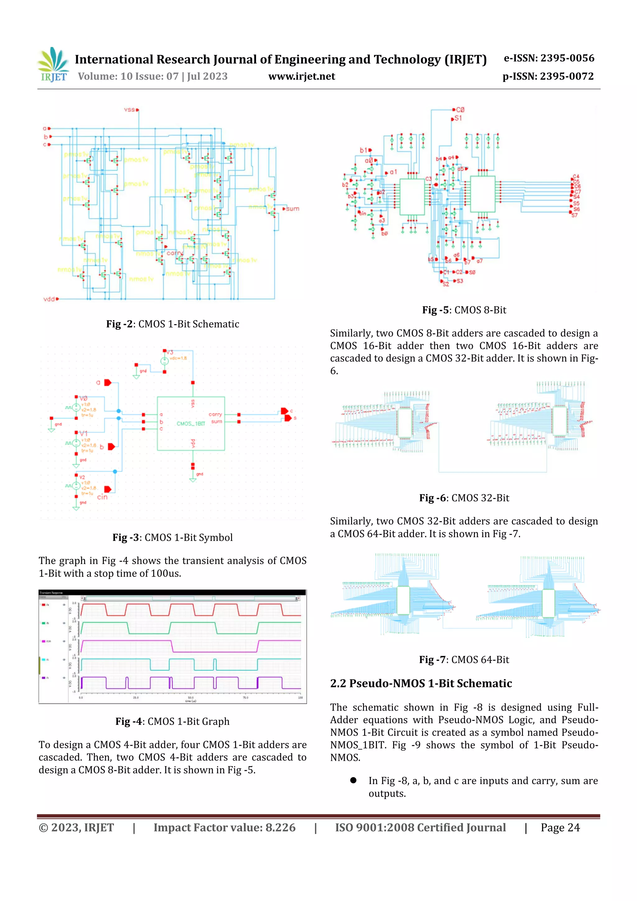
![International Research Journal of Engineering and Technology (IRJET) e-ISSN: 2395-0056
Volume: 10 Issue: 07 | Jul 2023 www.irjet.net p-ISSN: 2395-0072
© 2023, IRJET | Impact Factor value: 8.226 | ISO 9001:2008 Certified Journal | Page 27
Fig -18: Peak-Power value and Total-Power value of
Transmission Gate 64-Bit graph
3.2 Observations
Table -1: Power Analysis Table
Logic Family CMOS
Transmissio
n Gate
Pseudo-
NMOS
No. of
Transistor (64-
Bit)
1792 1024 1152
Average Power
(W)
14.94E-3 219.0E-6 14.94E-3
Total-Power
(W)
23.77mW 46.34uW 23.77mW
Peak-Power (W) 23.28mW 4.17mW 23.49mW
Delay (s) 107.608n 275.903p 107.608n
Power Delay
Product (PDP)
(J)
1.607E-09 6.0422E-14 1.607E-09
Based on our design, the Table -1 shows that the CMOS
logic family has the highest transistor count among the
three options, while the Transmission Gate logic family
has the lowest. However, the Transmission Gate logic
family exhibits the highest peak power consumption,
while the Pseudo-NMOS and CMOS families have identical
power consumption characteristics. In terms of delay, all
three logic families have the same value of 107.608 ns. The
power-delay product (PDP) is the lowest for the
Transmission Gate logic family, indicating better efficiency
in terms of power consumption and performance.
However, it may vary to different applications. We can
choose the desired logic family based on cost, power, and
performance.
4. CONCLUSIONS
Firstly, Transmission Gate Full-Adder circuits use fewer
transistors than CMOS and pseudo-NMOS Full-Adder
circuits. Secondly, Transmission Gate Full-Adder circuits
also have lower delays than other logic families. Thirdly,
Transmission Gate Full-Adders exhibit better power delay
product results than CMOS and Pseudo-NMOS Full-Adder
circuits; however, the choice of the logic family to be used
ultimately depends on the application's specific
requirements, such as cost, power and performance.
Hence, from our designs, these conclusions highlight the
advantages of using Transmission Gate Full-Adder circuits
in specific applications where power consumption and
delay are critical factors.
REFERENCES
[1] Ren, Y., & Liu, Y. (2013). A novel approach to improve
the performance of asynchronous circuit design using
self-timed circuit. CiteSeerX, 10.1.1.676.9601.
[2] Jampani, Y., & Gupta, G. B. (2022, July).
Implementation of 1-Bit full adder circuit using pass
transistor logic. IJRASET International Journal for
Research in Applied Science & Engineering
Technology, 10(7), 4974-4981.
doi:10.22214/ijraset.2022.46097
[3] Trapti Mittal and Uma Sharma, “ANALYSIS OF FULL
ADDER FOR POWER EFFICIENT CIRCUIT DESIGN”,
IJARSE Vol. No. 4, Issue 10, October 2015
[4] Manjunath K M, Abdul Lateef Haroon P S, A. Pagi and
Ulaganathan J, "Analysis of various full-adder circuits
in cadence," 2015 International Conference on
Emerging Research in Electronics, Computer Science
and Technology (ICERECT), Mandya, India, 2015, pp.
90-97, doi: 10.1109/ERECT.2015.7498994.
[5] Bhati, Ankita and Rita Jain. “Low Power Delay -
Product CMOS Full Adder.” (2015).
[6] G. R. Padmini, O. Rajesh, K. Raghu, N. M. Sree, C.
Apurva and K. saikumar, "Design and Analysis of 8-bit
ripple Carry Adder using nine Transistor Full Adder,"
2021 7th International Conference on Advanced
Computing and Communication Systems (ICACCS),
Coimbatore, India, 2021, pp. 1982-1987, doi:
10.1109/ICACCS51430.2021.9441928.
[7] Zitong Han 2021 J. Phys.: Conf. Ser. 1754 012131
[8] Karunakaran, S., & Poonguzharselvi, B. (2017, March).
Exploration on power delay product of basic logic
gates for various CMOS logic styles. International
Journal of Engineering Studies, 9(2), 111-120.
doi:10.11648/j.ijes.20170902.12](https://crownmelresort.com/image.slidesharecdn.com/irjet-v10i704-230815101719-b3fcba46/75/Design-And-Analysis-Of-64-Bit-Adders-In-Cadence-Using-Different-Logic-Families-6-2048.jpg)

The document describes the design and analysis of 64-bit adders using different logic families in Cadence. Specifically, it discusses: 1. Implementing 1-bit full adder circuits using CMOS, Pseudo-NMOS, and Transmission Gate logic and cascading them to create 64-bit adders of each family. 2. Simulating and analyzing the power consumption of the 64-bit adders, measuring their total power, peak power, and power-delay product. 3. Finding that CMOS and Pseudo-NMOS have identical power characteristics while Transmission Gate has the highest peak power but lowest transistor count and power-delay product.