What is ASIC Design?
ASIC = Application-Specific Integrated Circuit
These are chips made for a specific purpose (ex: camera sensor chip, WiFi chip).
The design process goes from writing code → checking → converting to hardware → final layout.
---
About the Company (Vivartan Technologies LLP)
Started in 2016, Bangalore.
Works on VLSI design & training.
Helps students learn industry tools through hands-on projects.
---
Standard Cell Design
Standard cells = small building blocks of a chip (like LEGO pieces).
Examples: inverters, AND, OR, XOR, buffers.
Designed using transistors and optimized for speed & power.
---
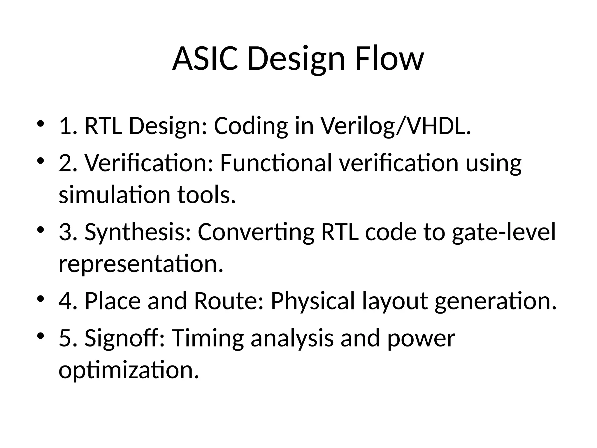
ASIC Design Flow (Main Steps)
1. RTL Design:
Write hardware code in Verilog/VHDL.
2. Verification:
Simulate and check if the code works correctly.
3. Synthesis:
Convert code into a gate-level circuit.
4. Place & Route (Physical Design):
Arrange the cells on a chip and connect them.
5. Signoff:
Final checks: timing, power, design rules.
---
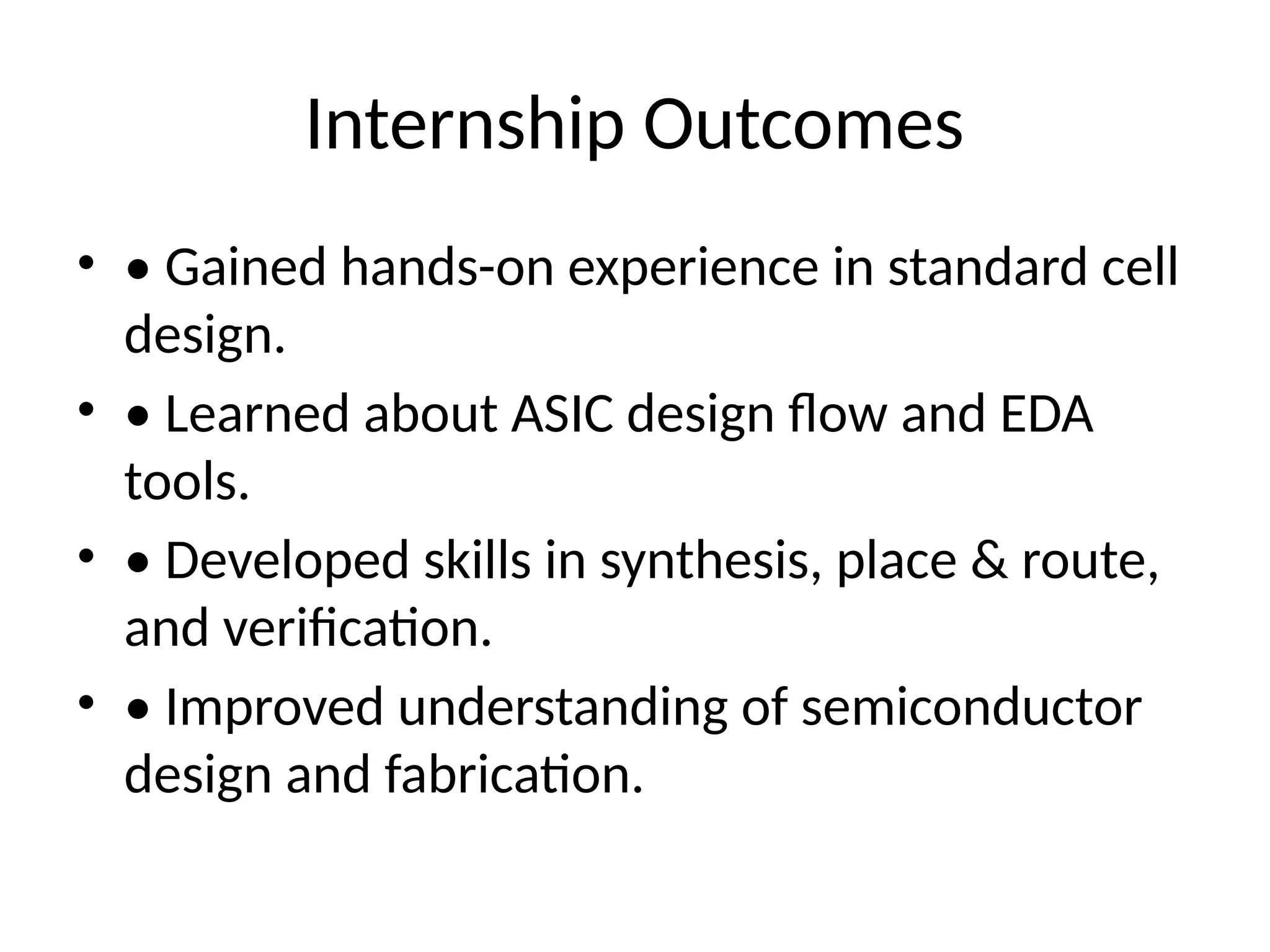
Internship Outcomes
Learned how standard cells are created.
Understood the complete ASIC flow from RTL → GDS.
Gained hands-on experience with EDA tools.
Improved knowledge of chip design process.
---
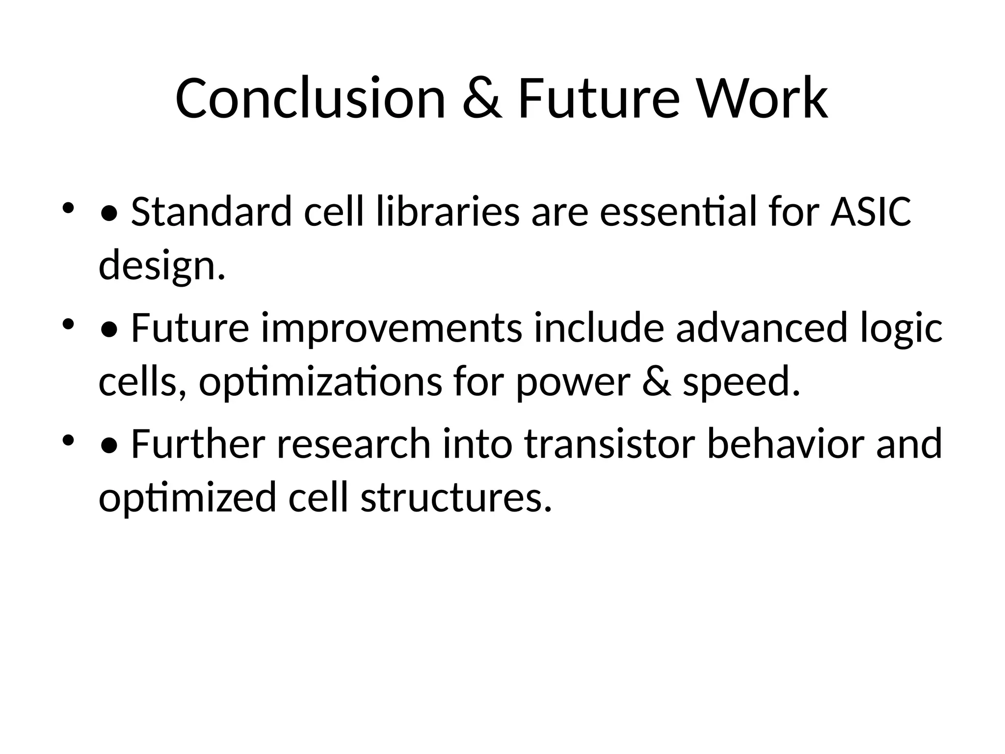
Conclusion
Standard cell libraries are crucial for ASICs.
Future work:
Better cell designs
More power & speed optimizations
More research on transistor behavior


![Cse iii-logic design [10 cs33]-notes](https://cdn.slidesharecdn.com/ss_thumbnails/cse-iii-logicdesign10cs33-notes-150811132805-lva1-app6892-thumbnail.jpg?width=640&height=640&fit=bounds)


![Laminated_Springs[1]. Machine design practice](https://cdn.slidesharecdn.com/ss_thumbnails/laminatedsprings1-251116120255-2a3c06fb-thumbnail.jpg?width=640&height=640&fit=bounds)


