The document provides an overview of VLSI front-end design, emphasizing the evolution of integration from SSI to VLSI and discussing specific applications such as ASIC and SoC designs. It outlines the design flow involved in creating complex integrated circuits, including stages like architecture, RTL coding, verification, and physical design. Additionally, it highlights the roles and expectations of design and verification engineers within the semiconductor industry.
An introduction to the VLSI front design, focusing on the foundational aspects of integrated circuit design.
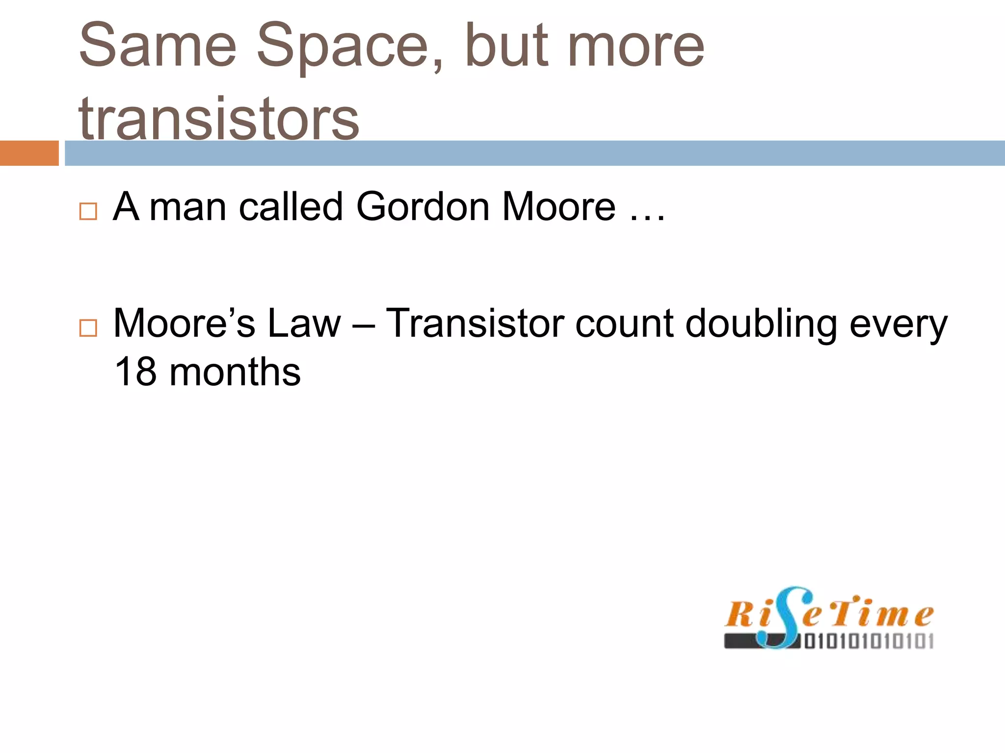
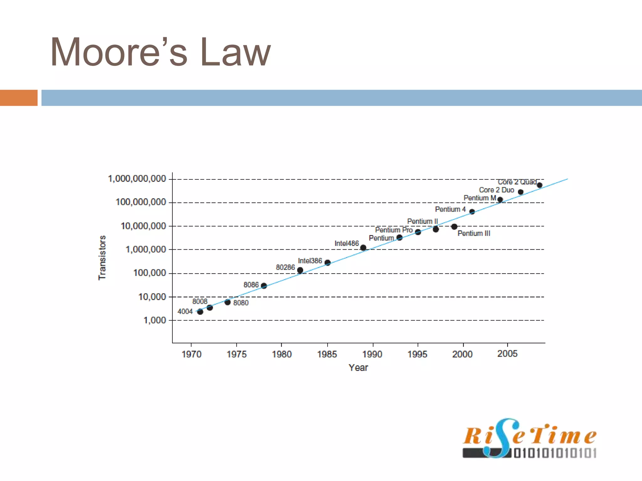
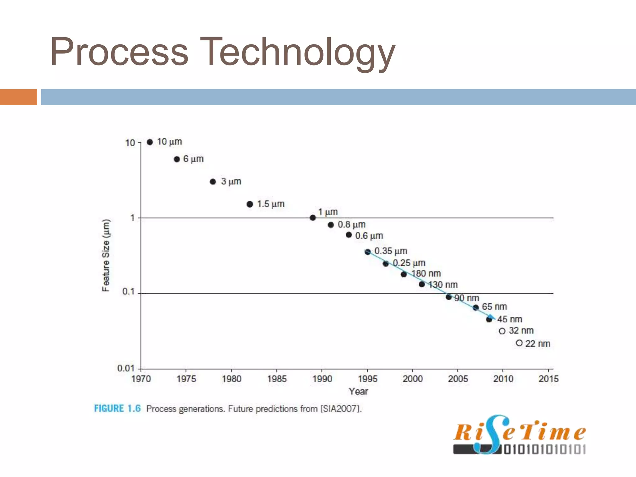
Discussion of transistor scaling (SSI to VLSI), Moore's Law, and complexities in ASIC and SoC design.
Differences between Application Specific Integrated Circuits (ASICs) and System on Chip (SoC) designs, emphasizing functionalities.
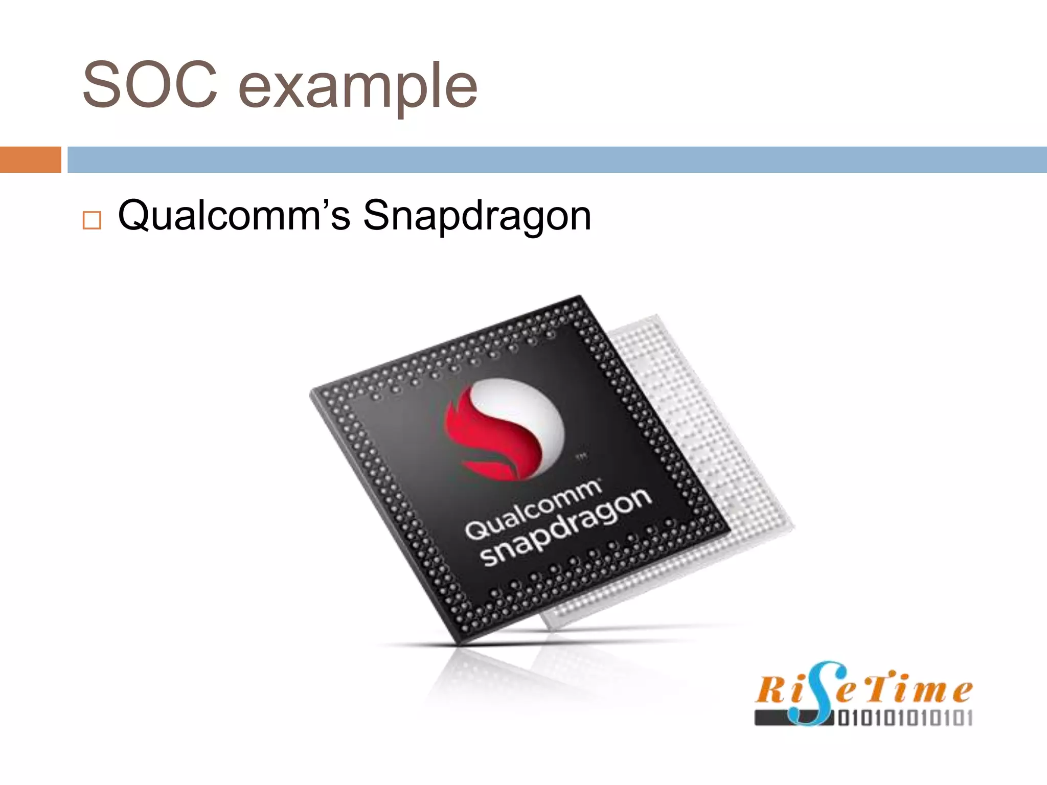
Case study of Qualcomm's Snapdragon as an example of a complex SoC integrating various functionalities.
Detailed explanation of ASIC design flow, including specification, architecture, RTL coding, verification, synthesis, and physical design. Converting designs from RTL to gate-level and the physical design process in chip layout, culminating in tape-out.
Clarification of front-end processes leading to netlist generation versus back-end processes up to layout.
Responsibilities of ASIC/SOC design and verification engineers, emphasizing skills in digital design and testbench creation.
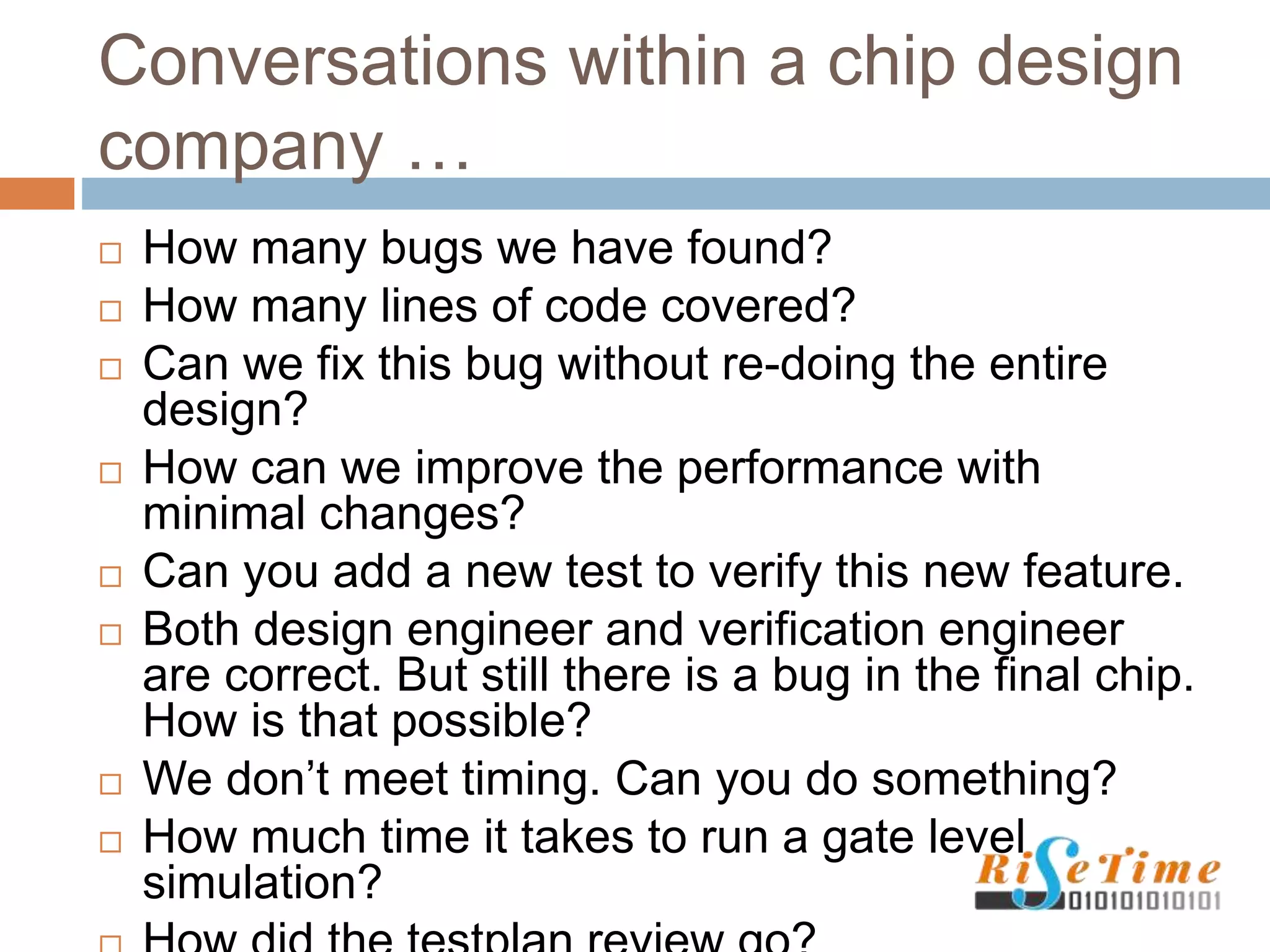
Common issues faced in semiconductor design companies such as bug tracking, performance improvements, and team communications.
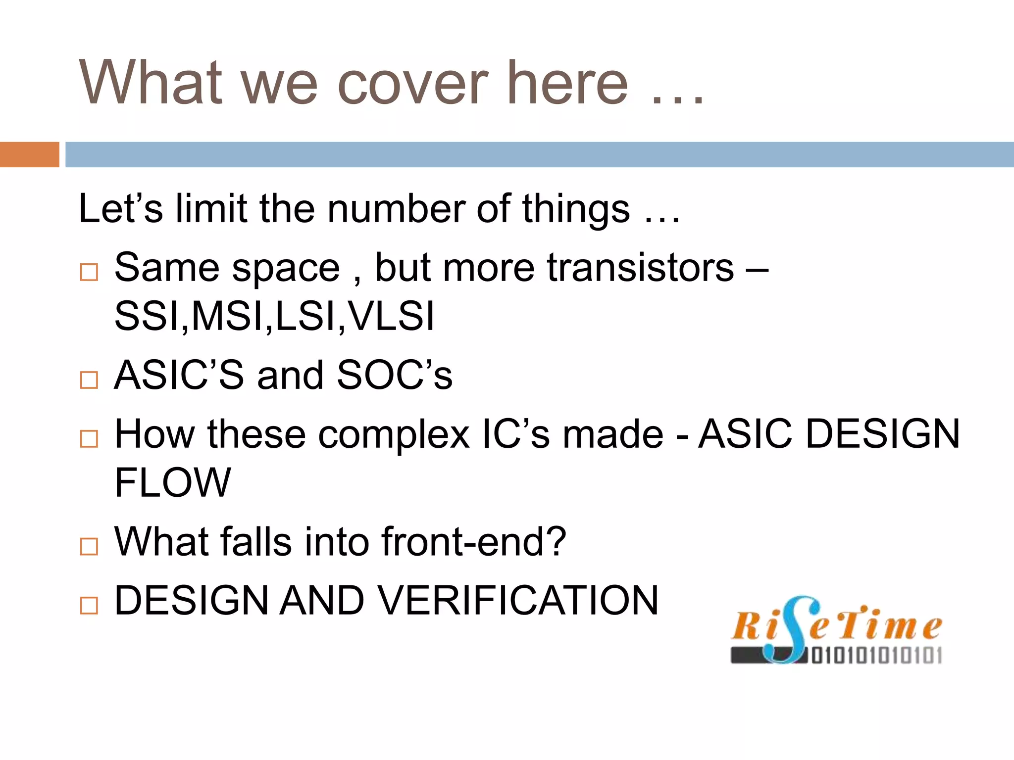
What we coverhere …
Let’s limit the number of things …
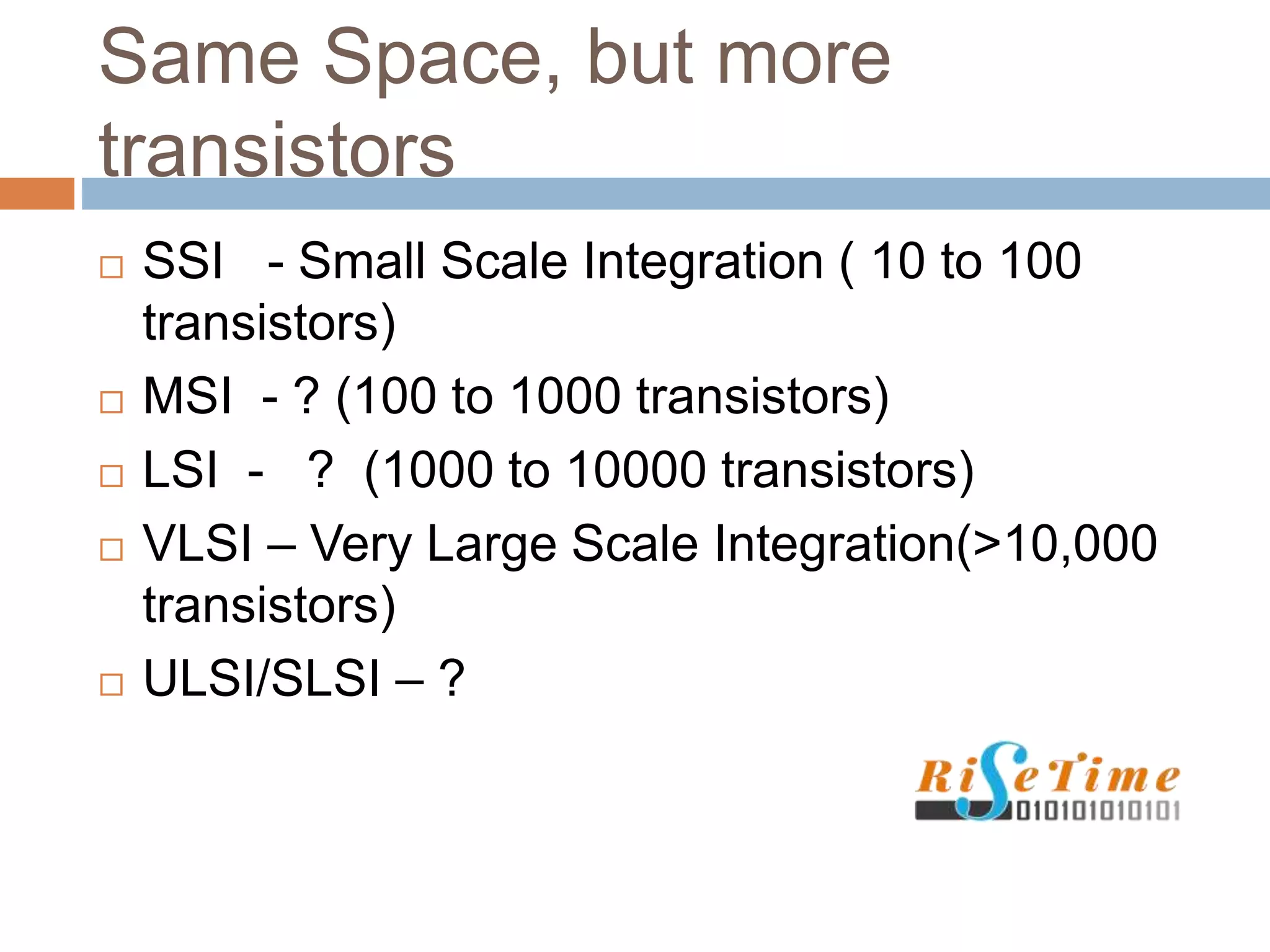
Same space , but more transistors –
SSI,MSI,LSI,VLSI
ASIC’S and SOC’s
How these complex IC’s made - ASIC DESIGN
FLOW
What falls into front-end?
DESIGN AND VERIFICATION
Same Space, butmore
transistors
SSI - Small Scale Integration ( 10 to 100
transistors)
MSI - ? (100 to 1000 transistors)
LSI - ? (1000 to 10000 transistors)
VLSI – Very Large Scale Integration(>10,000
transistors)
ULSI/SLSI – ?
9.
What we coverhere …
Same space , but more transistors –
SSI,MSI,LSI,VLSI
ASIC’S and SOC’s
How these complex IC’s made - ASIC DESIGN
FLOW
What falls into front-end?
DESIGN AND VERIFICATION
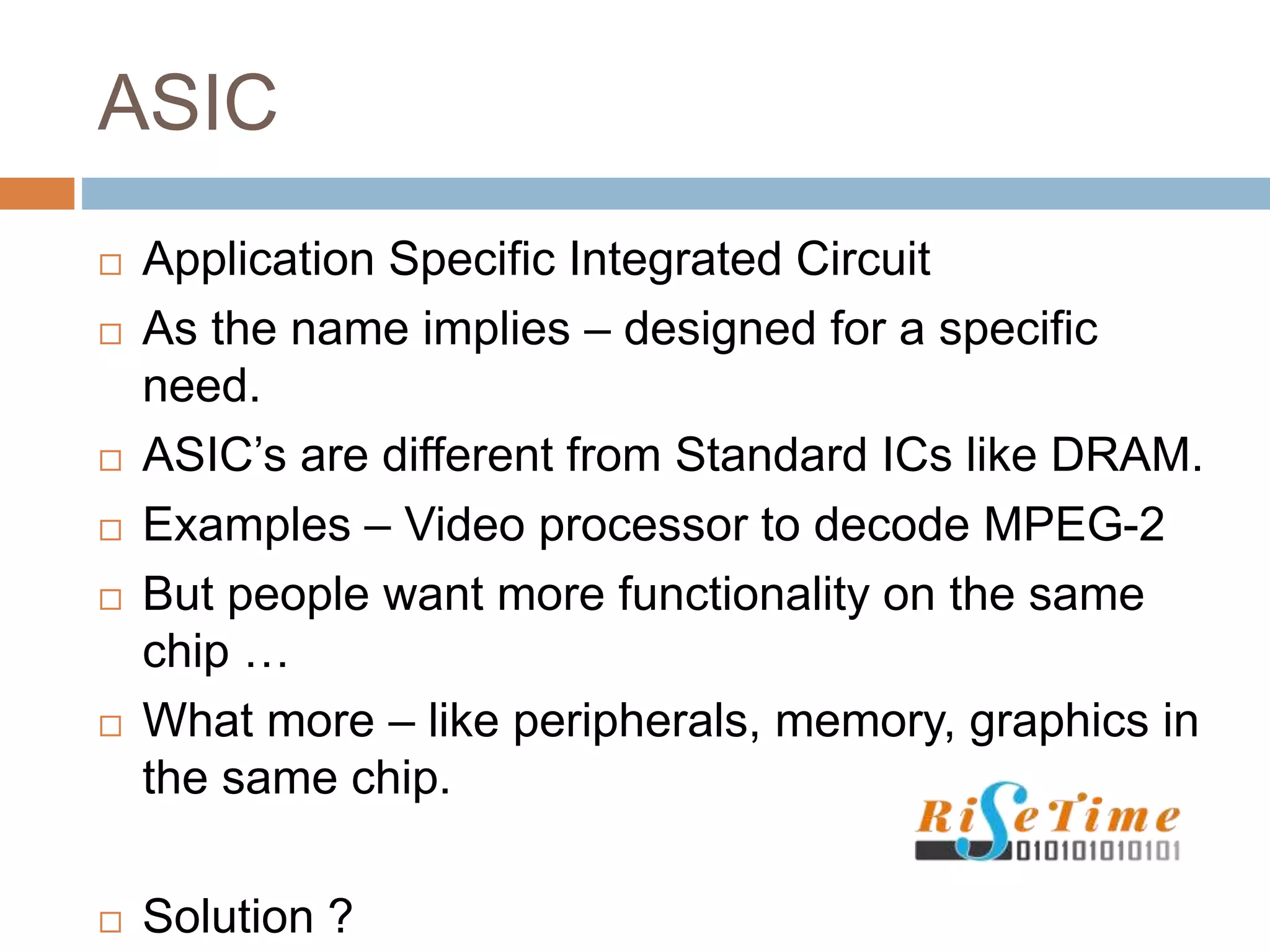
ASIC
Application SpecificIntegrated Circuit
As the name implies – designed for a specific
need.
ASIC’s are different from Standard ICs like DRAM.
Examples – Video processor to decode MPEG-2
But people want more functionality on the same
chip …
What more – like peripherals, memory, graphics in
the same chip.
Solution ?
12.
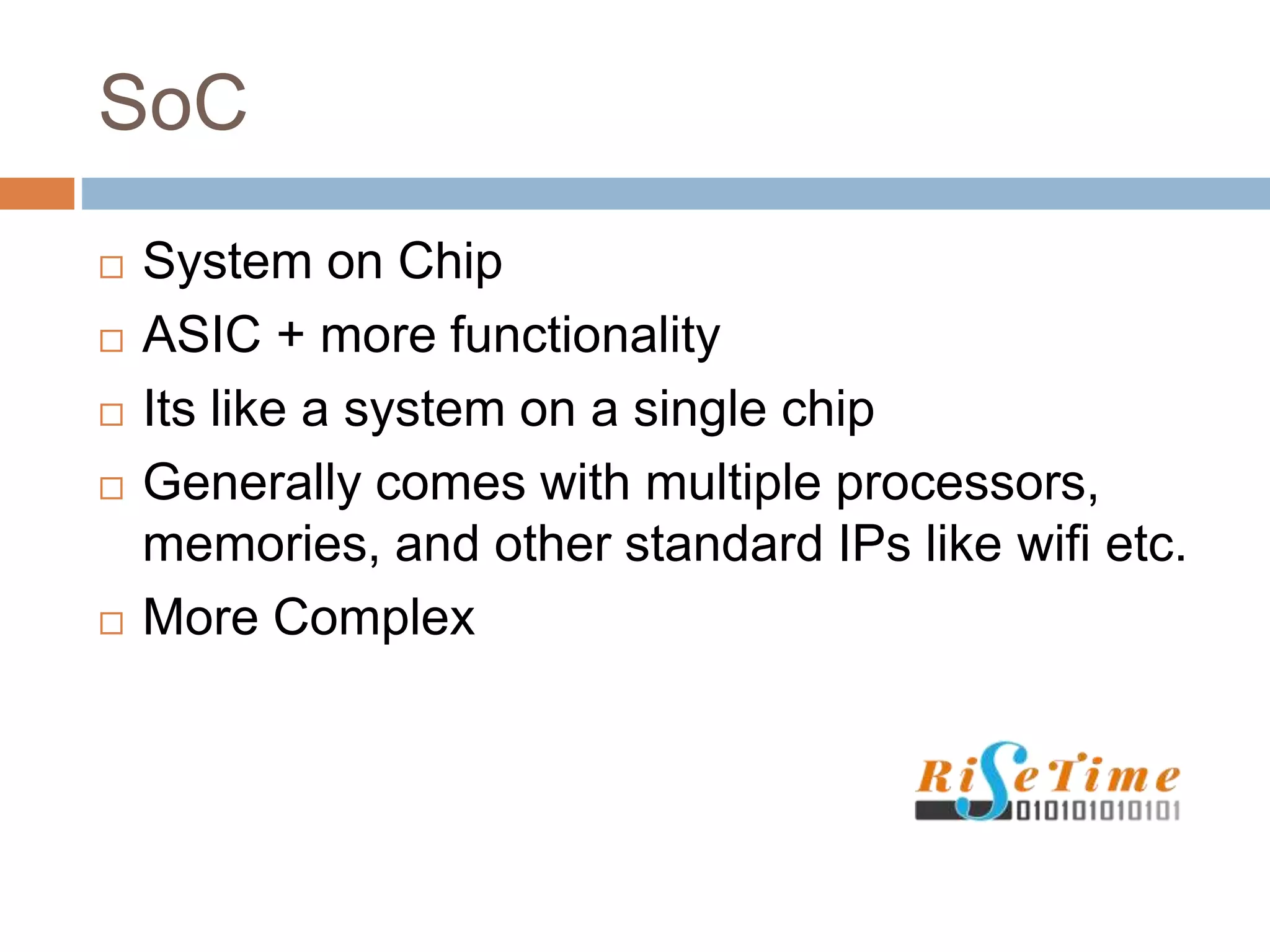
SoC
System onChip
ASIC + more functionality
Its like a system on a single chip
Generally comes with multiple processors,
memories, and other standard IPs like wifi etc.
More Complex
What we coverhere …
Same space , but more transistors –
SSI,MSI,LSI,VLSI
ASIC’S and SOC’s
How these complex IC’s made - ASIC DESIGN
FLOW
What falls into front-end?
DESIGN AND VERIFICATION
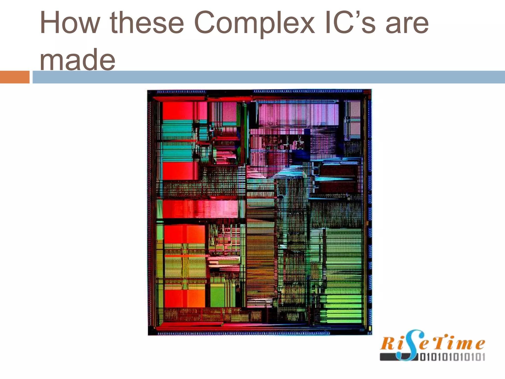
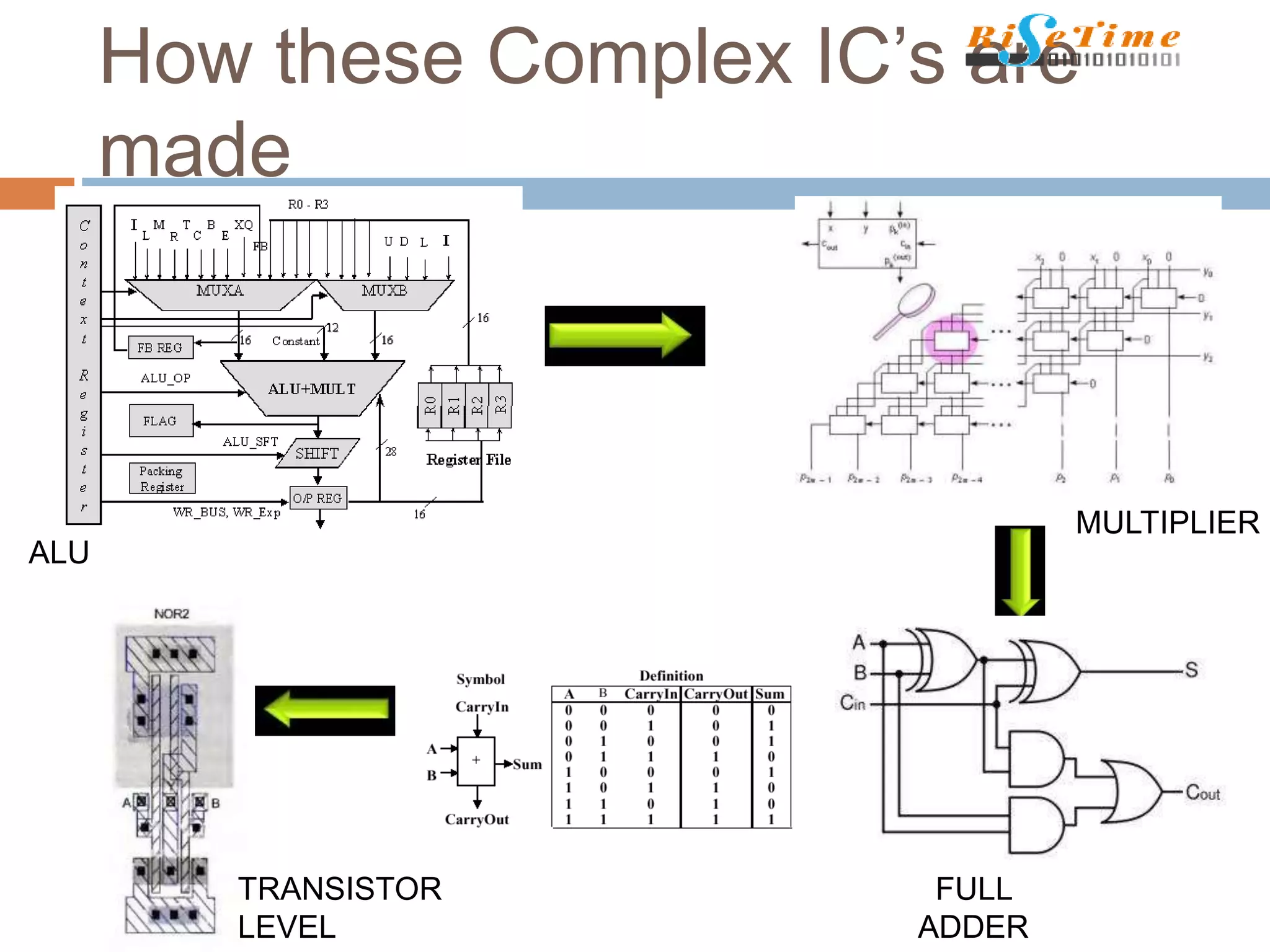
How these ComplexIC’s are
made
ALU
MULTIPLIER
FULL
ADDER
TRANSISTOR
LEVEL
19.
How these ComplexIC’s are
made
Chip functionality – what is expected of
ASIC/SoC
Not just functionality – Speed , power, Cost
etc., are the main factors that beat your
competition
I/O requirements – How will the ASIC
communicate with outside world.
Design Specification – a list of requirements to
meet
Architecture
Design
Architecture
Different architecturesare considered to
maximize performance factors below …
Area
Speed
Throughput
Latency
Best Architecture is chosen that optimizes all
parameters.
22.
Design
No moreHand-drawn designs
RTL(Register Transfer Language) Descriptions
HDLs(Hardware Description Languages) –
Verilog and VHDL
Describe the design in Verilog(or vhdl)
23.
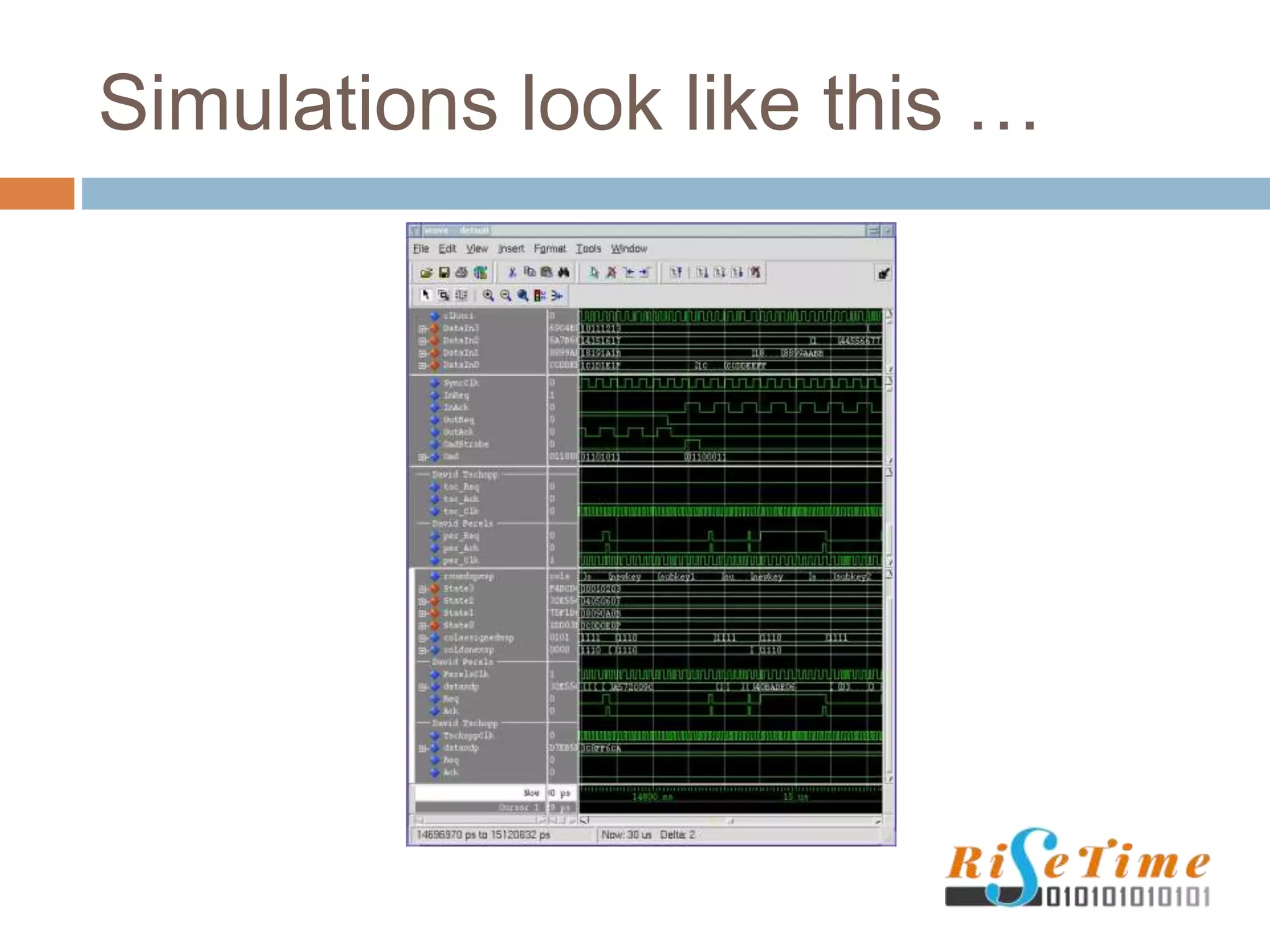
Verification
How doyou know your design functions as
expected?
Develop a testbench
Generate Stimulus
Simulating your design
Verify your design
How many bugs have you found?
When do you say “Verification is complete”
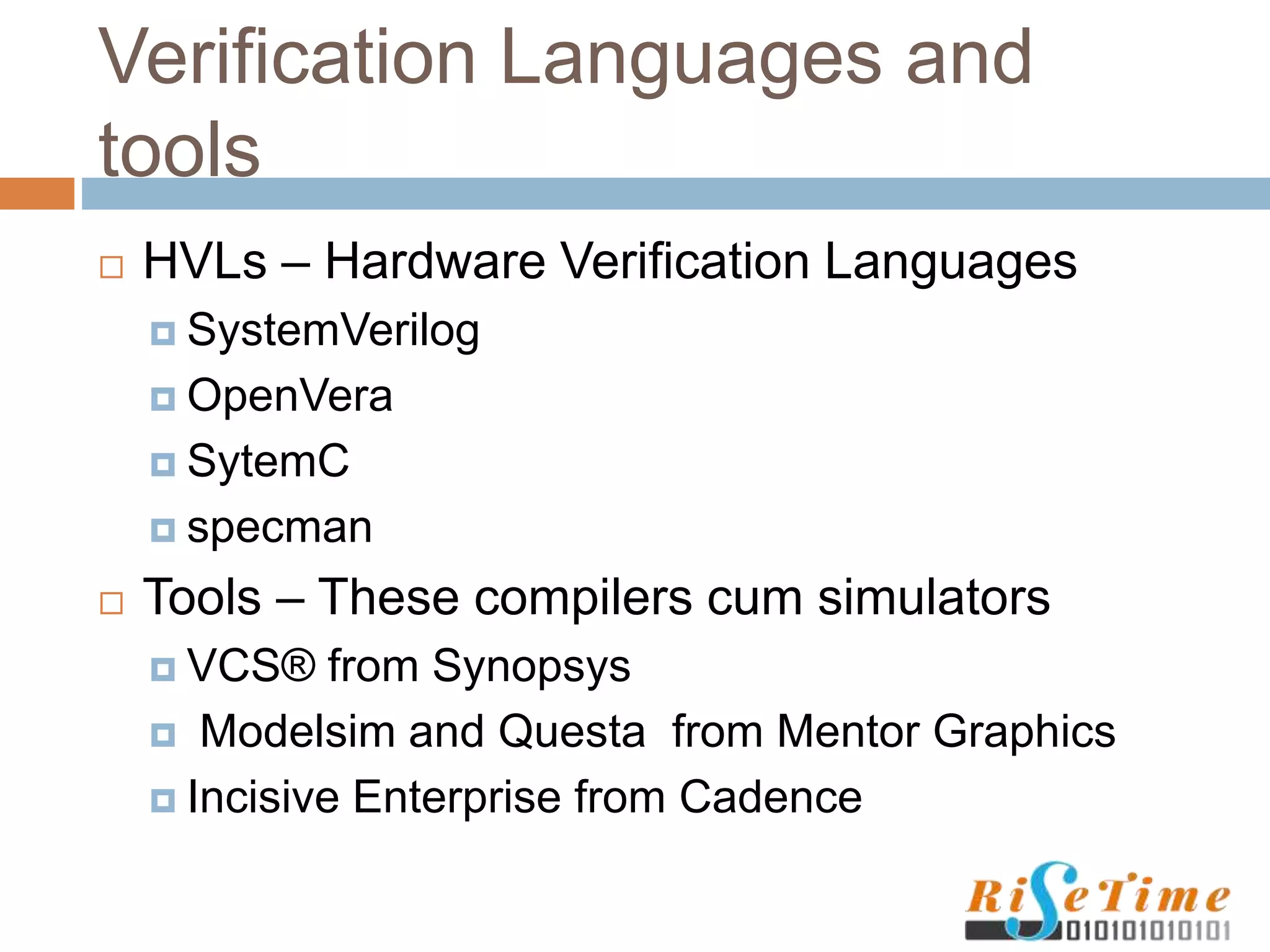
Verification Languages and
tools
HVLs – Hardware Verification Languages
SystemVerilog
OpenVera
SytemC
specman
Tools – These compilers cum simulators
VCS® from Synopsys
Modelsim and Questa from Mentor Graphics
Incisive Enterprise from Cadence
27.
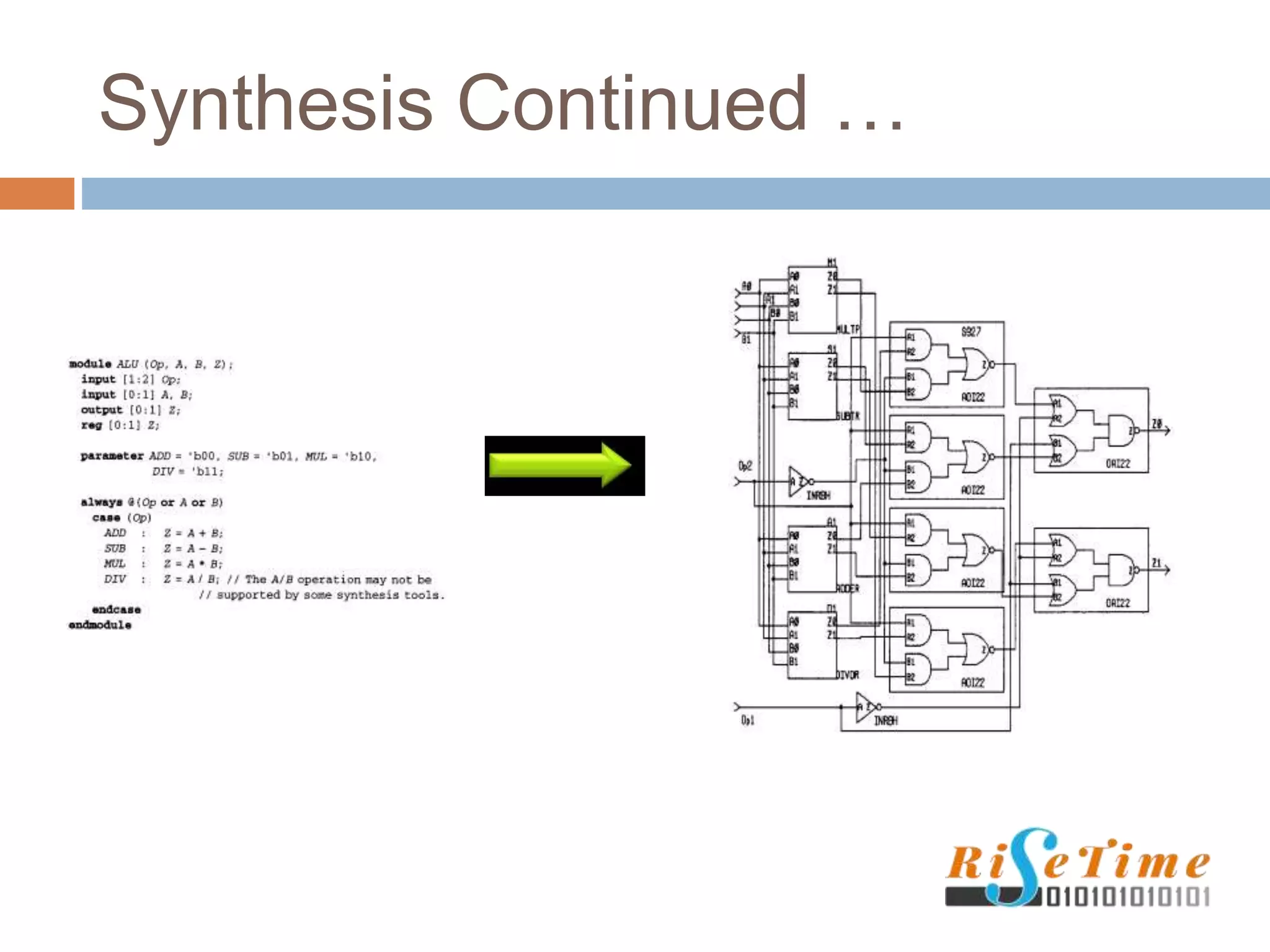
Synthesis
Now youhave design and it is verified.
But Your design is in verilog description
Convert it into gates.
The Process of converting RTL to Netlist is
called synthesis.
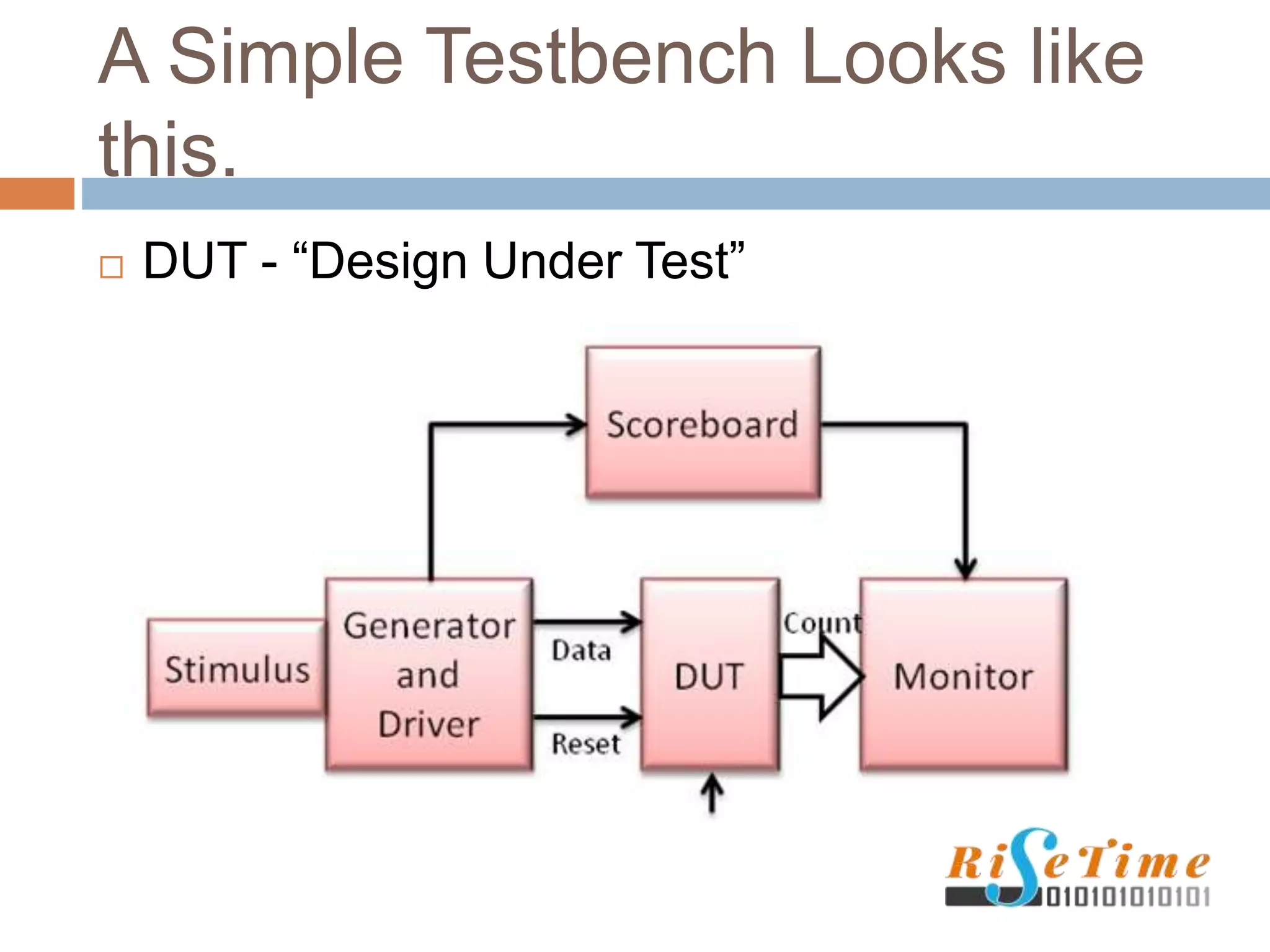
A Picture is worth million words ...
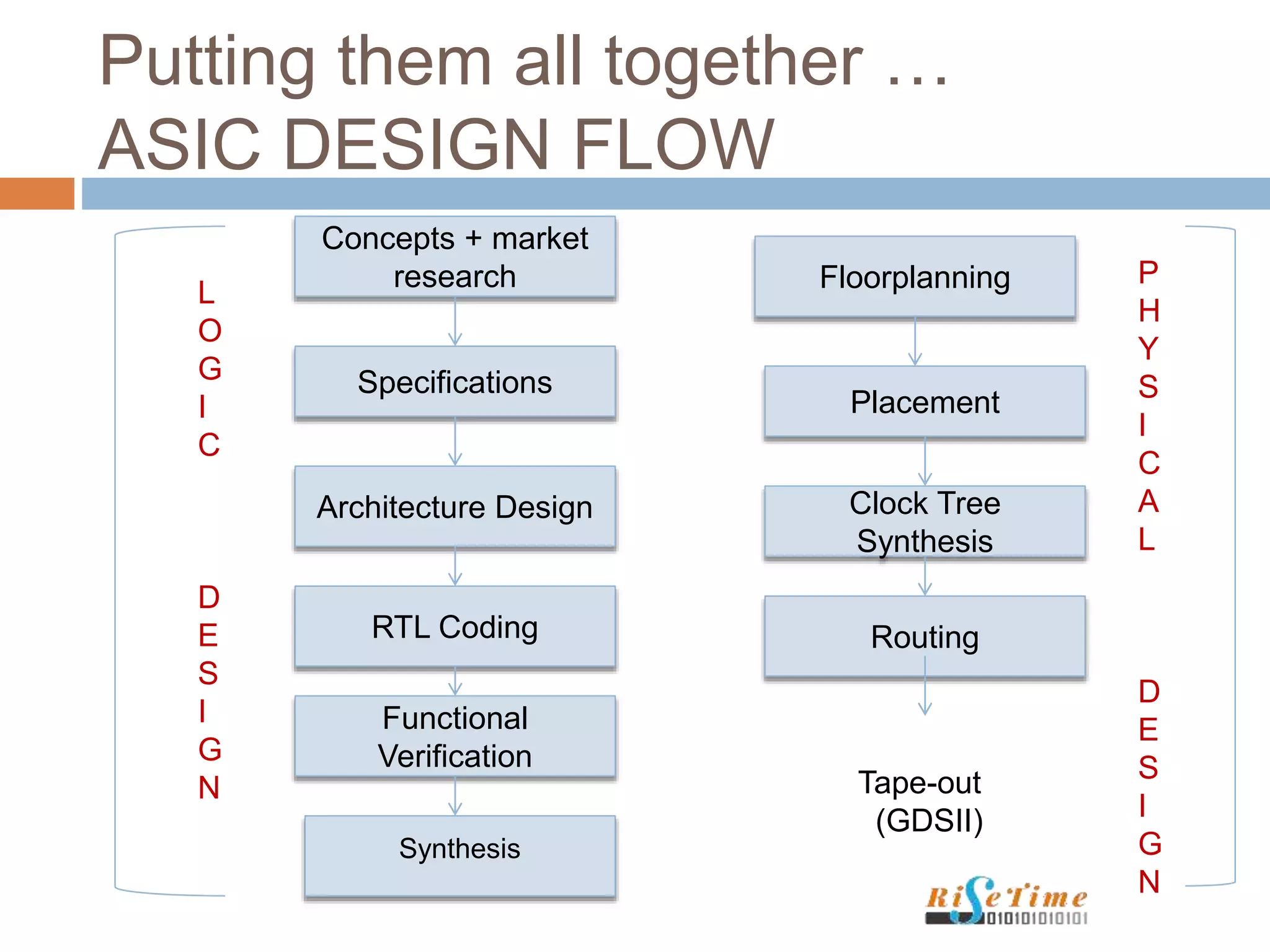
Putting them alltogether …
ASIC DESIGN FLOW
Concepts + market
research
Synthesis
Specifications
Architecture Design
RTL Coding
Functional
Verification
L
O
G
I
C
D
E
S
I
G
N
Floorplanning
Placement
Routing
Tape-out
(GDSII)
P
H
Y
S
I
C
A
L
D
E
S
I
G
N
Clock Tree
Synthesis
30.
Physical Design
Onceyou have the netlist, place them on the
silicon?
Physical design refers to all steps that convert
Circuit representation into a geometric
representation(layout)
In Simple words, fitting the design onto the
given area of silicon, meeting all requirements
like speed etc., and not violating the design
rules imposed by foundry.
Send the GDSII to fab to manufacture the chip.
What we coverhere …
Same space , but more transistors –
SSI,MSI,LSI,VLSI
ASIC’S and SOC’s
How these complex IC’s made - ASIC DESIGN
FLOW
What falls into front-end?
DESIGN AND VERIFICATION
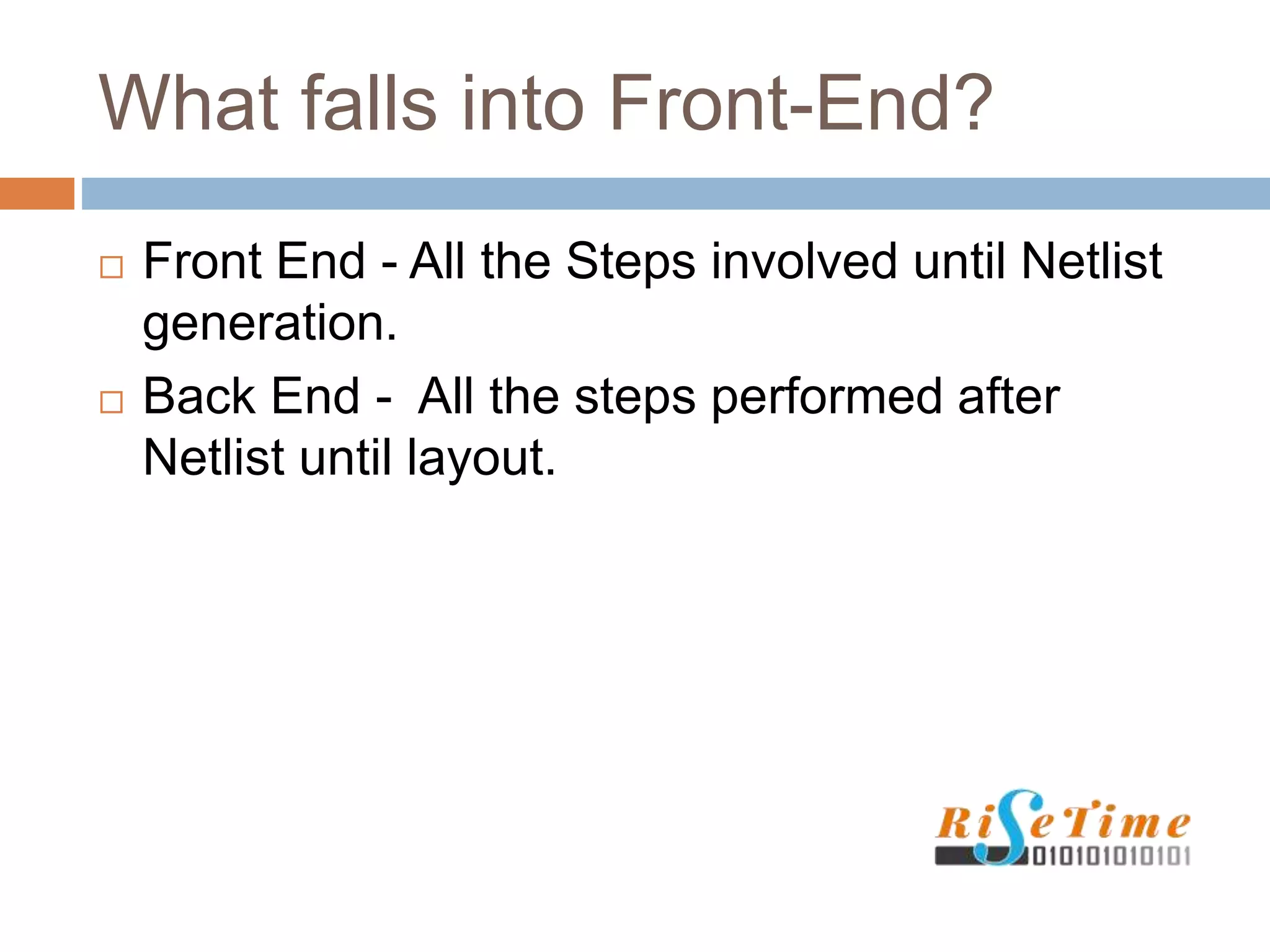
What falls intoFront-End?
Front End - All the Steps involved until Netlist
generation.
Back End - All the steps performed after
Netlist until layout.
35.
What we coverhere …
Same space , but more transistors –
SSI,MSI,LSI,VLSI
ASIC’S and SOC’s
How these complex IC’s made - ASIC DESIGN
FLOW
What falls into front-end?
DESIGN AND VERIFICATION
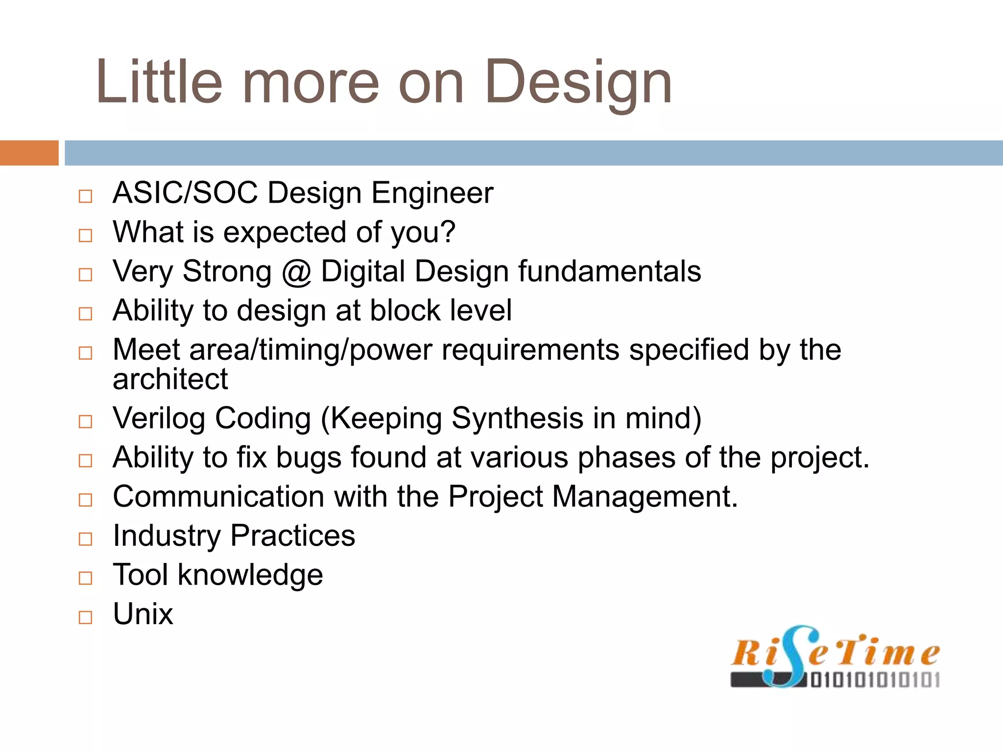
Little more onDesign
ASIC/SOC Design Engineer
What is expected of you?
Very Strong @ Digital Design fundamentals
Ability to design at block level
Meet area/timing/power requirements specified by the
architect
Verilog Coding (Keeping Synthesis in mind)
Ability to fix bugs found at various phases of the project.
Communication with the Project Management.
Industry Practices
Tool knowledge
Unix
38.
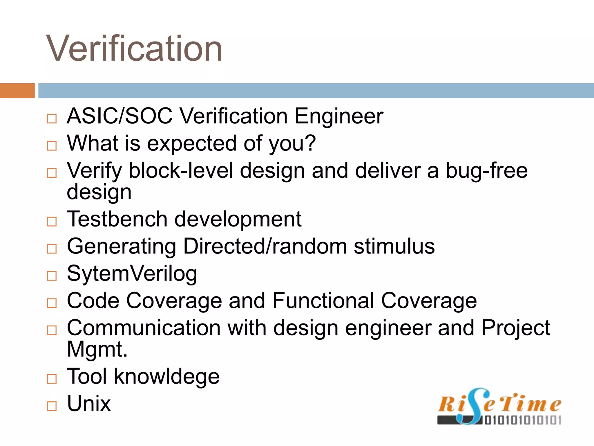
Verification
ASIC/SOC VerificationEngineer
What is expected of you?
Verify block-level design and deliver a bug-free
design
Testbench development
Generating Directed/random stimulus
SytemVerilog
Code Coverage and Functional Coverage
Communication with design engineer and Project
Mgmt.
Tool knowldege
Unix
39.
What we coverhere …
Same space , but more transistors –
SSI,MSI,LSI,VLSI
ASIC’S and SOC’s
How these complex IC’s made - ASIC DESIGN
FLOW
What falls into front-end?
DESIGN AND VERIFICATION
Conversations within achip design
company …
How many bugs we have found?
How many lines of code covered?
Can we fix this bug without re-doing the entire
design?
How can we improve the performance with
minimal changes?
Can you add a new test to verify this new feature.
Both design engineer and verification engineer
are correct. But still there is a bug in the final chip.
How is that possible?
We don’t meet timing. Can you do something?
How much time it takes to run a gate level
simulation?