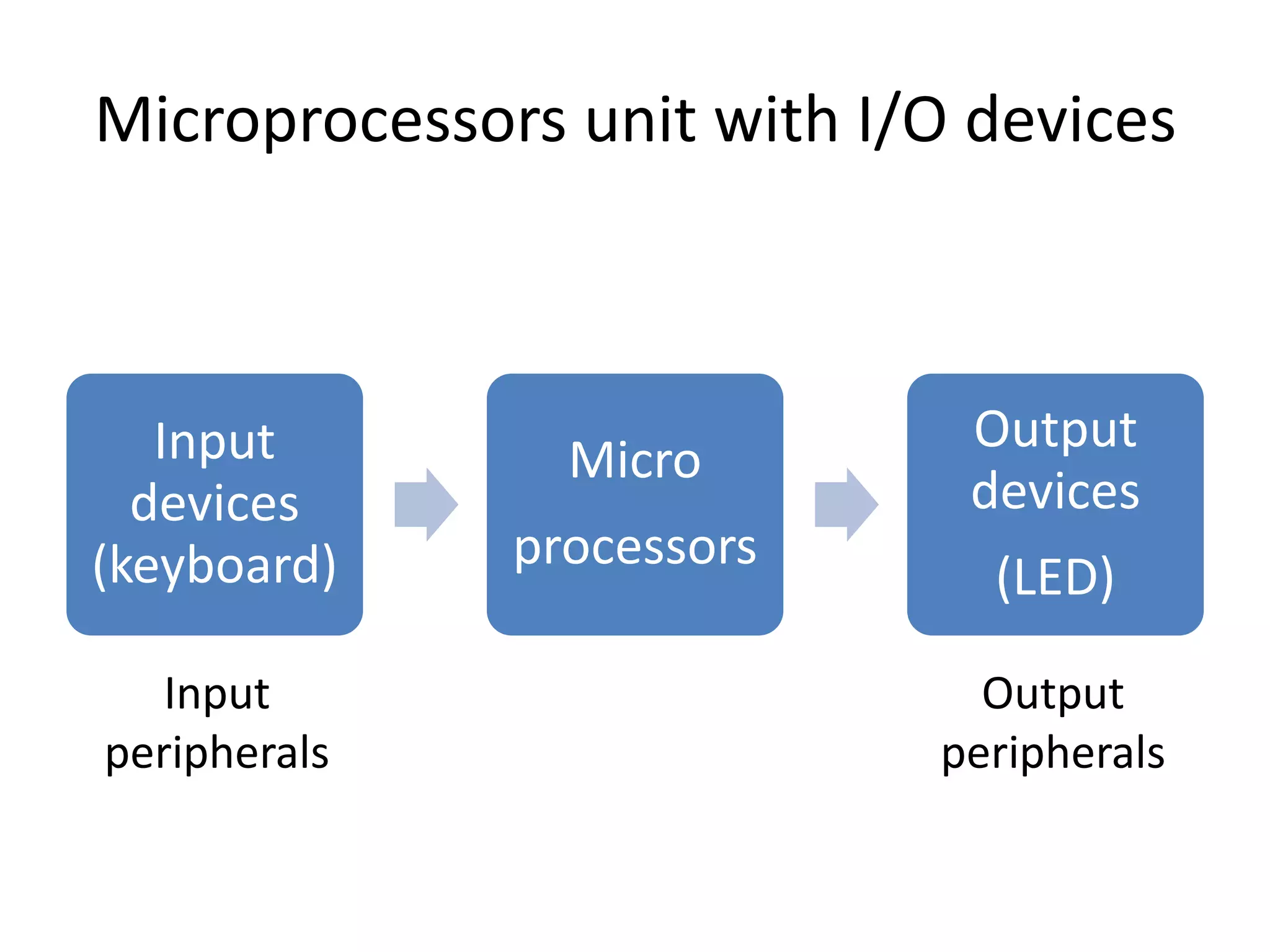
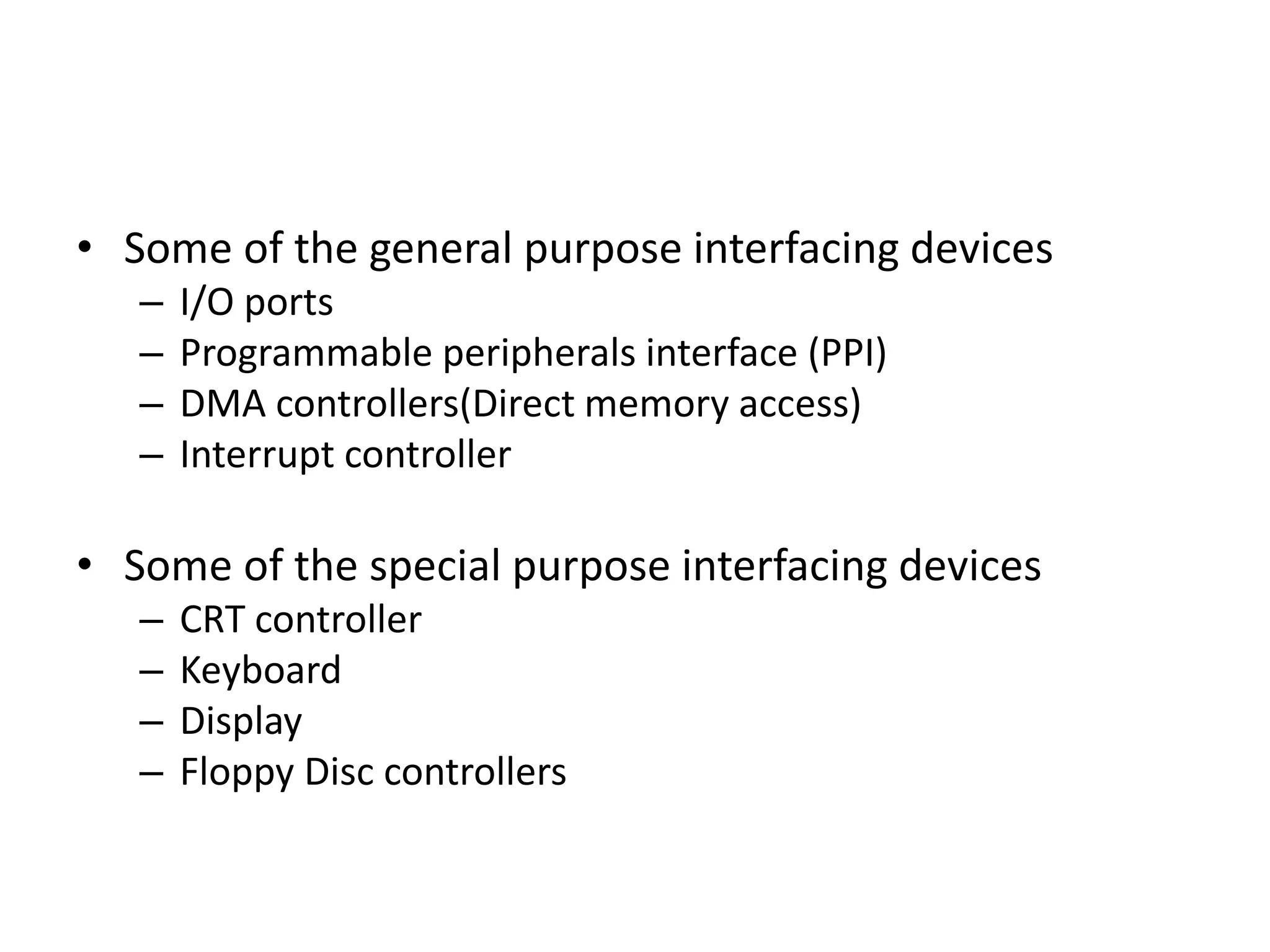
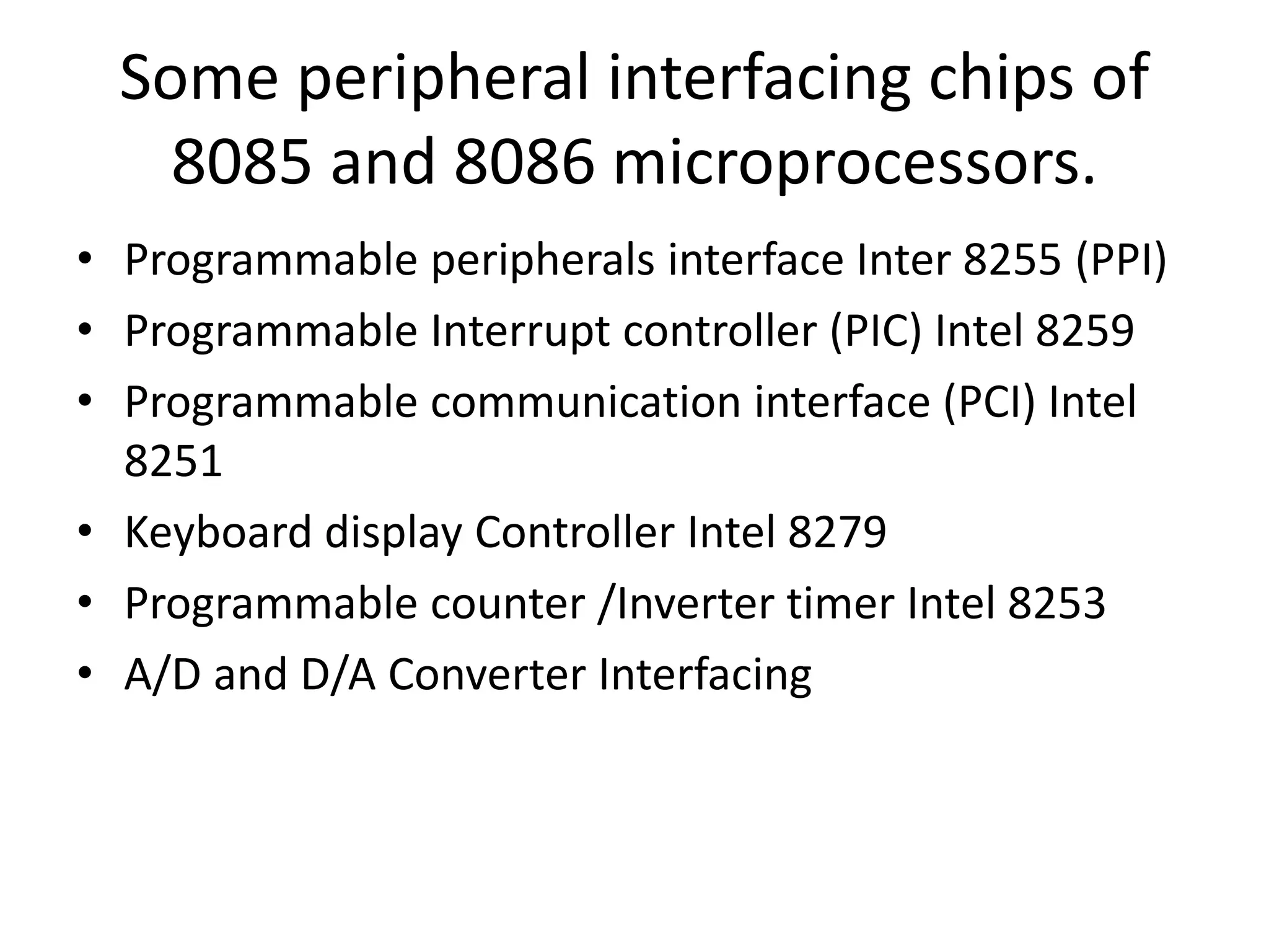
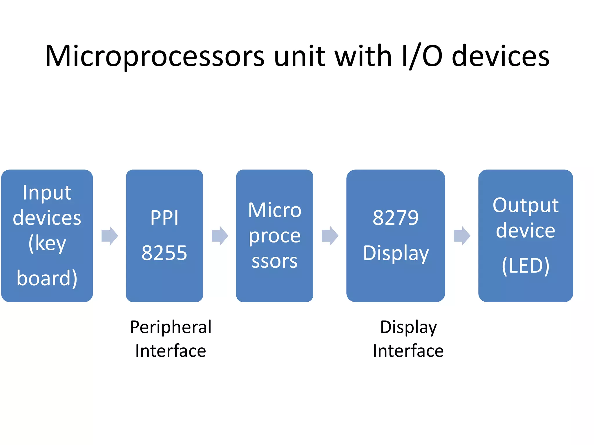
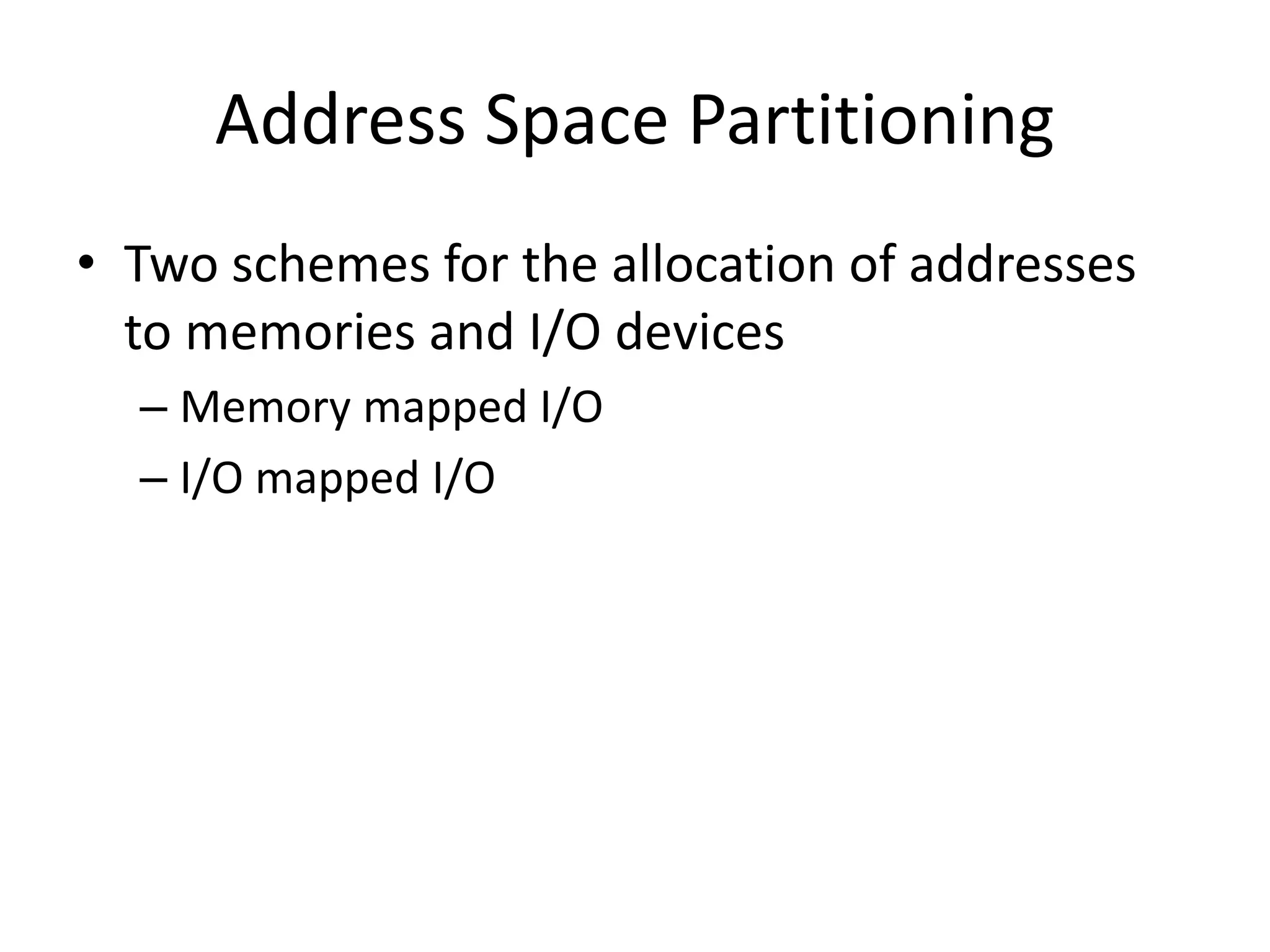
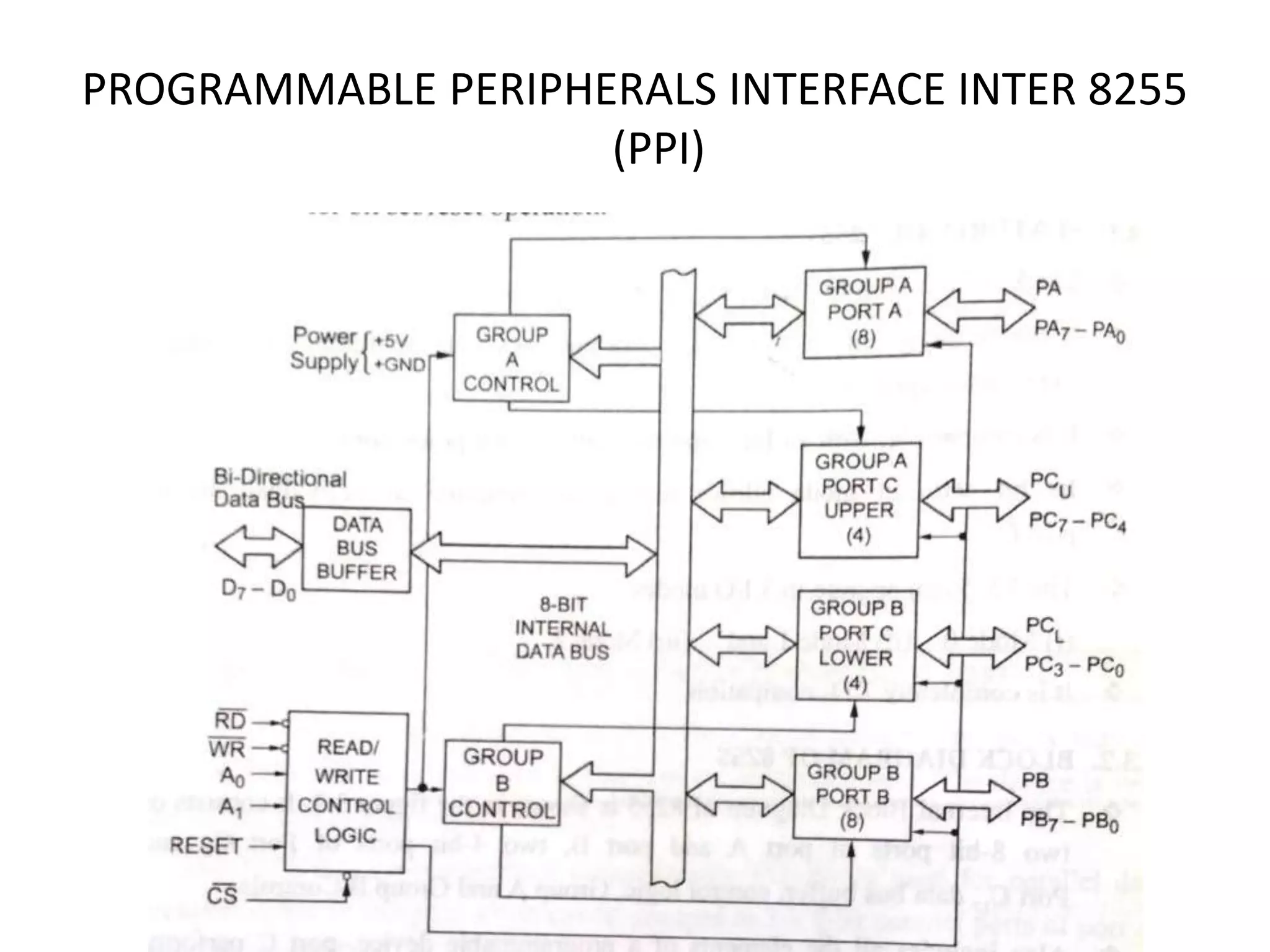
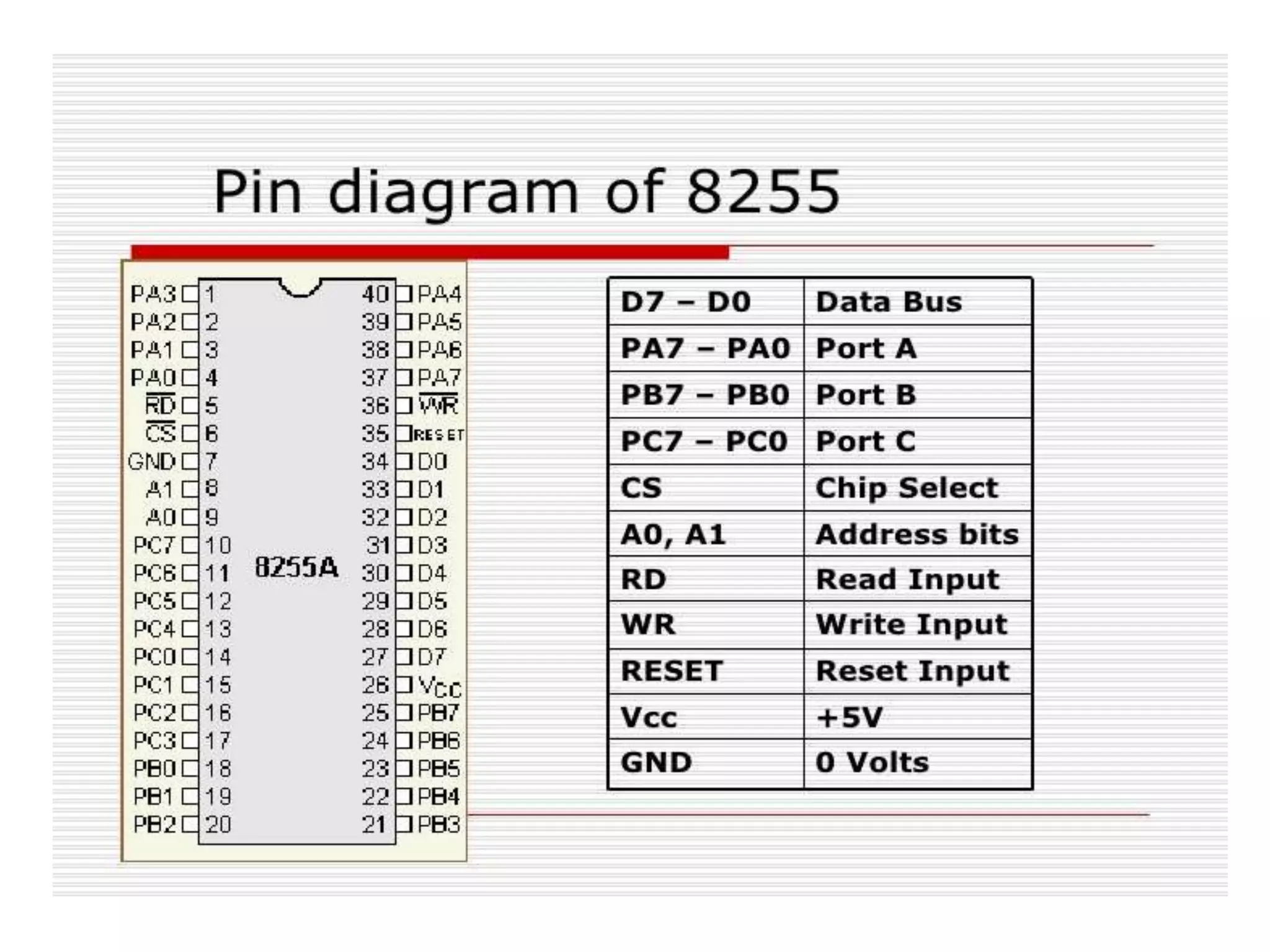
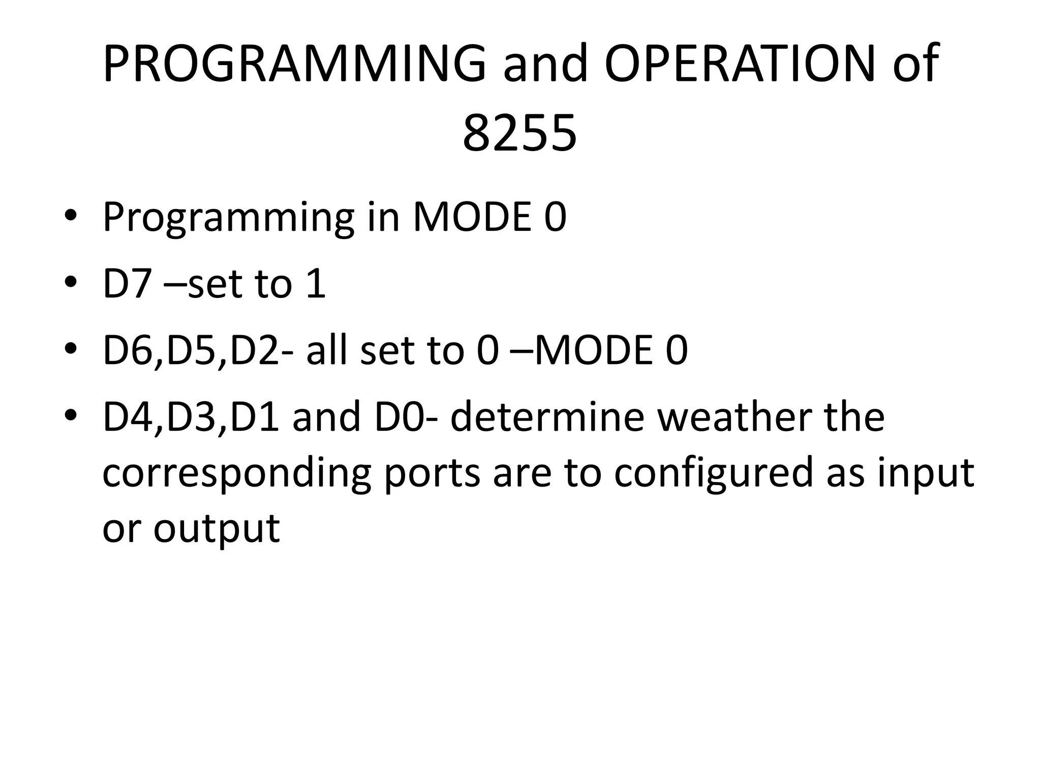
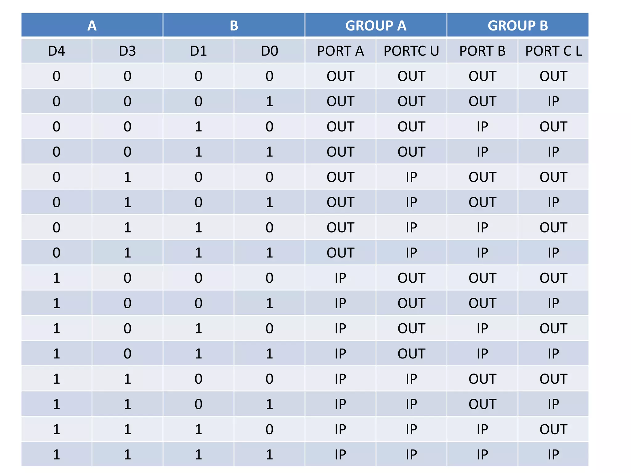
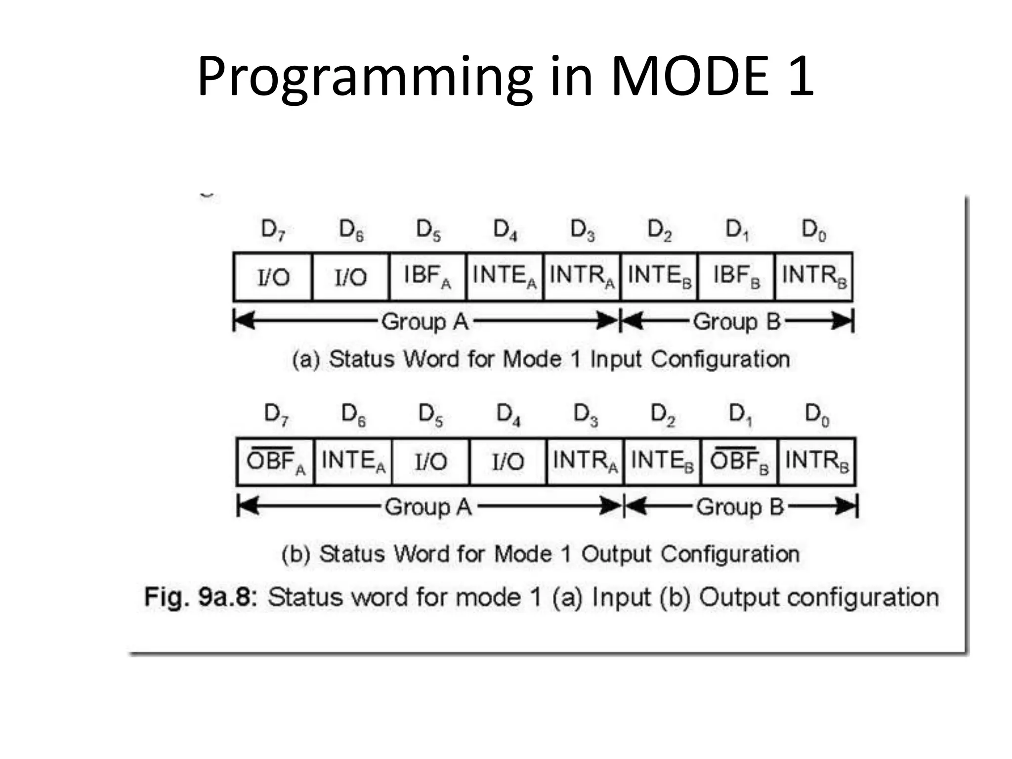
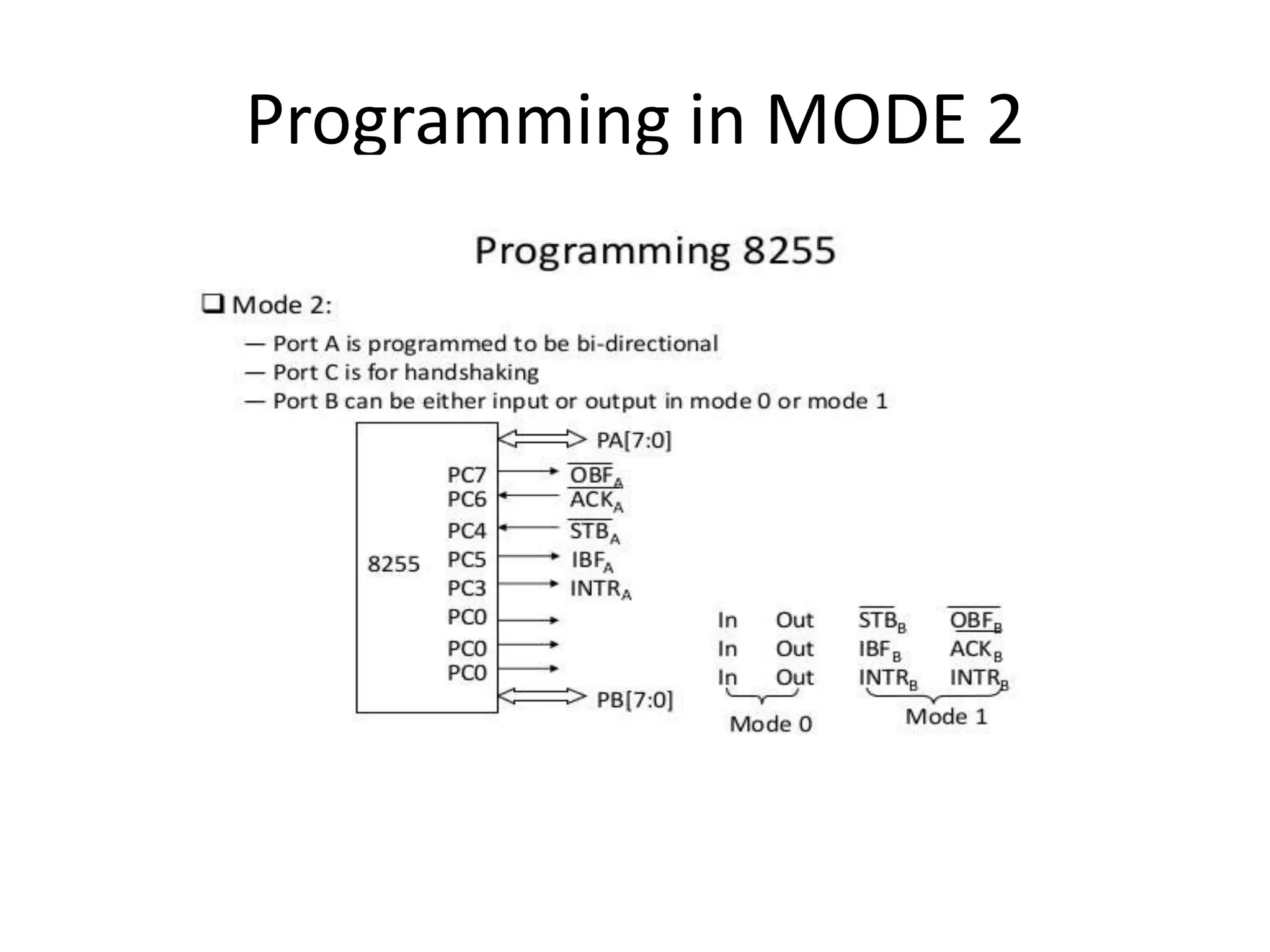
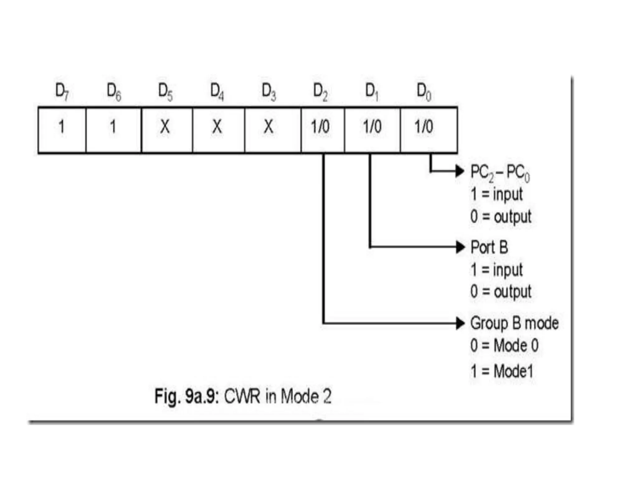
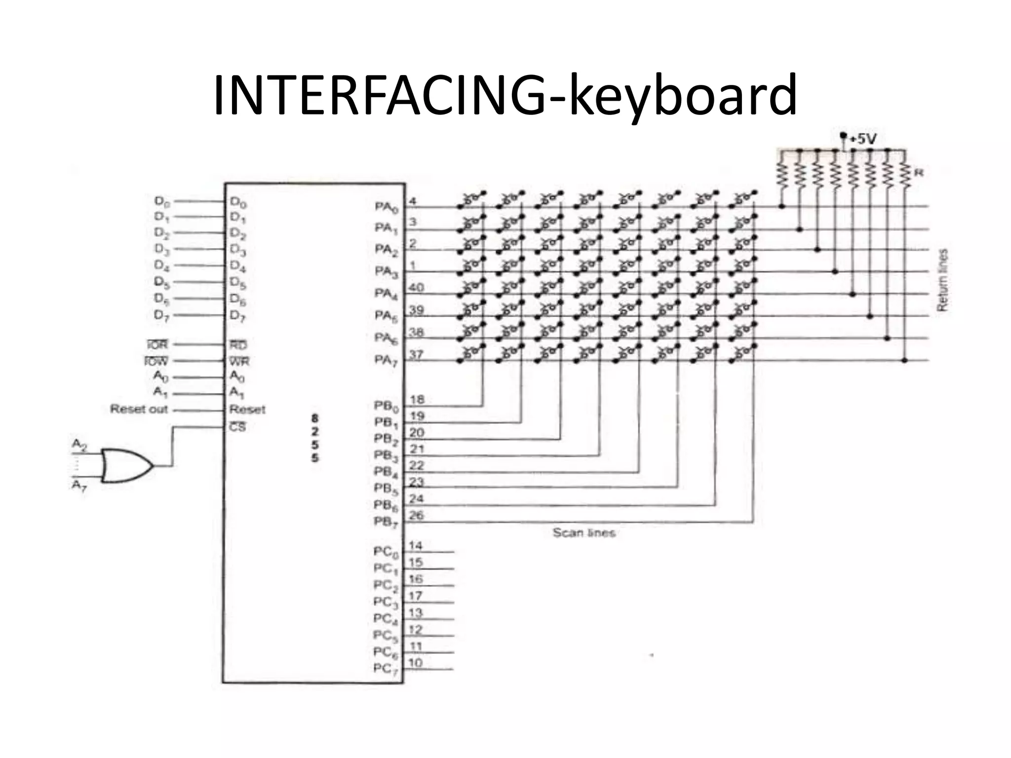
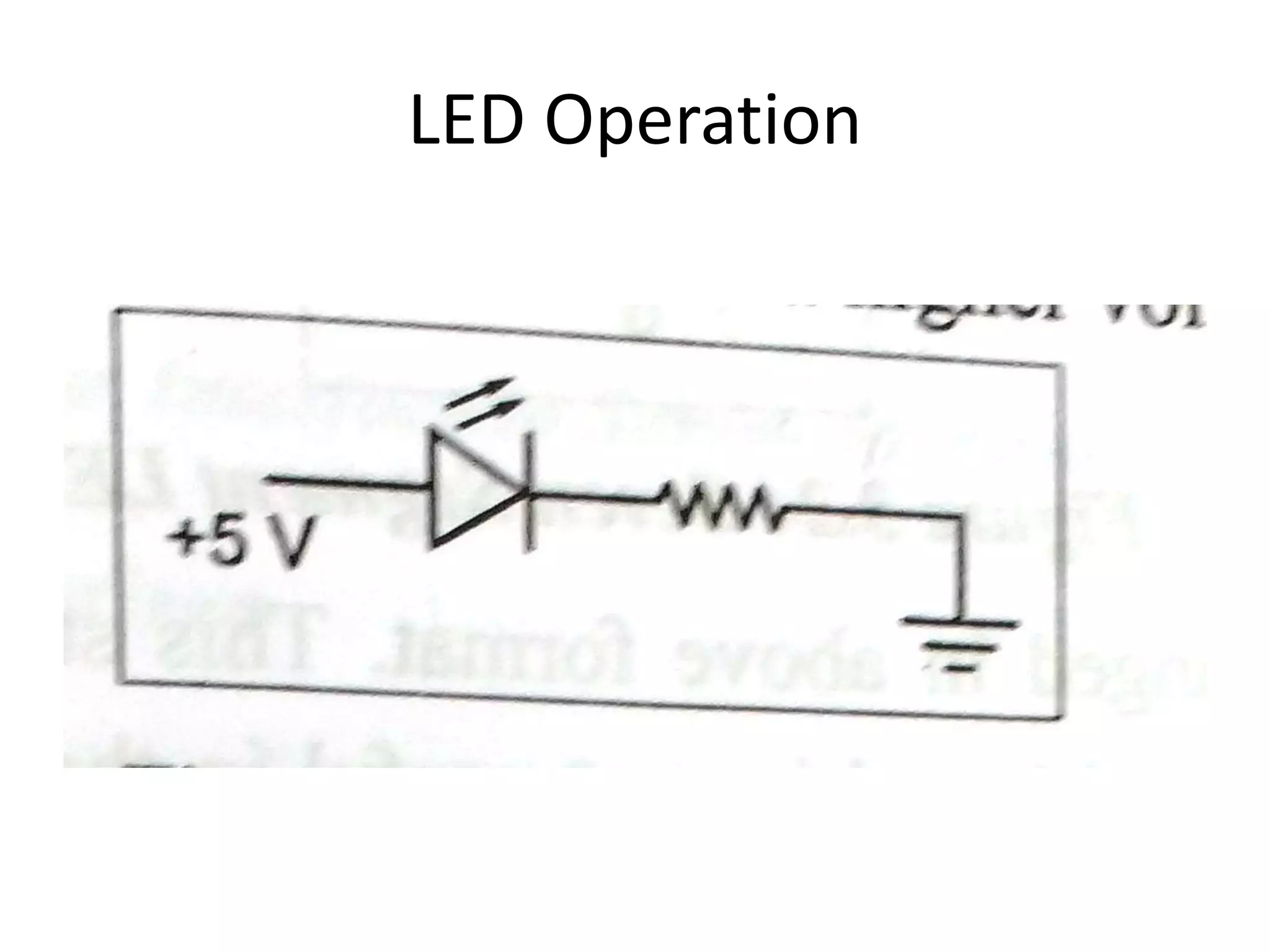
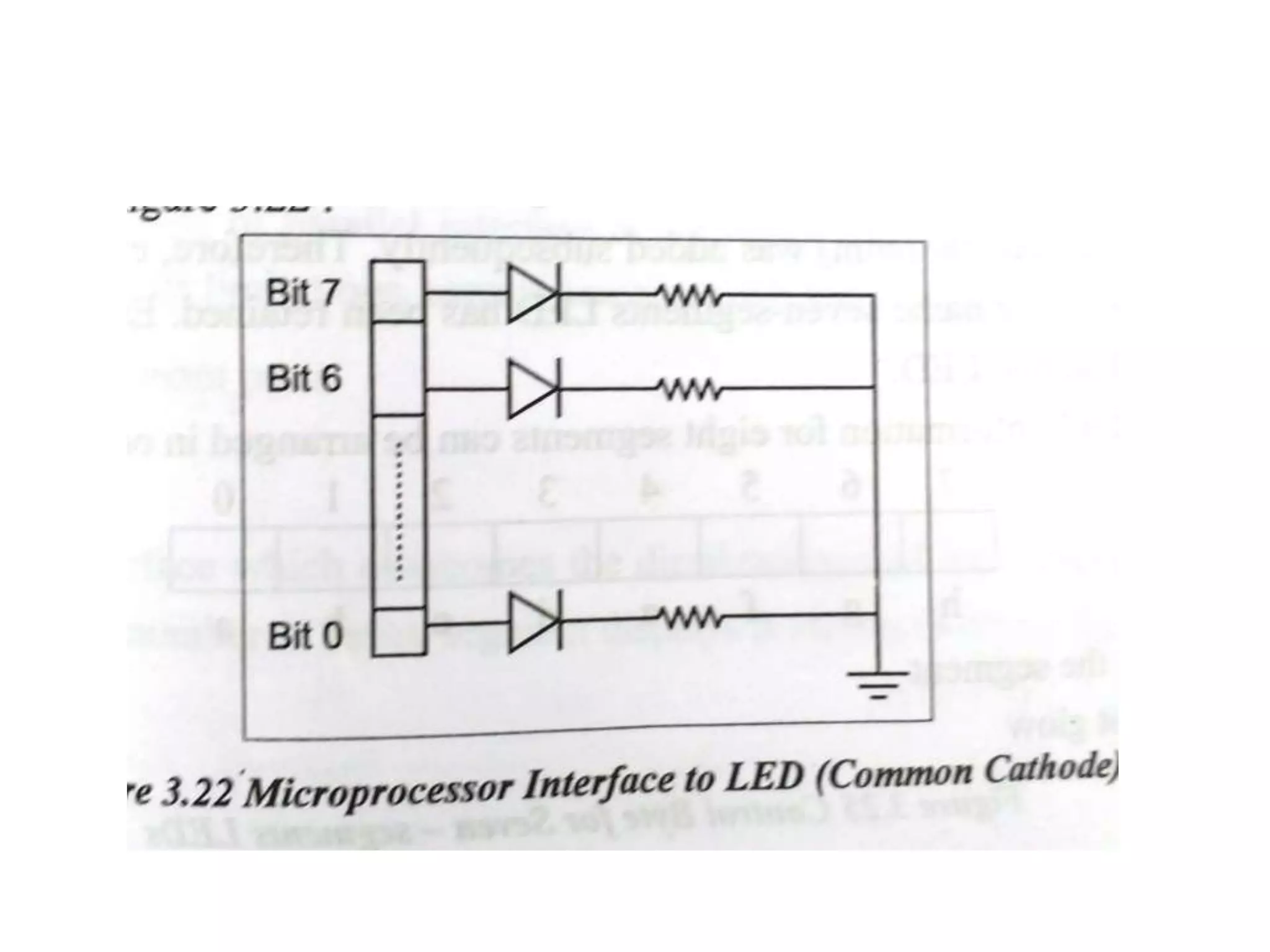
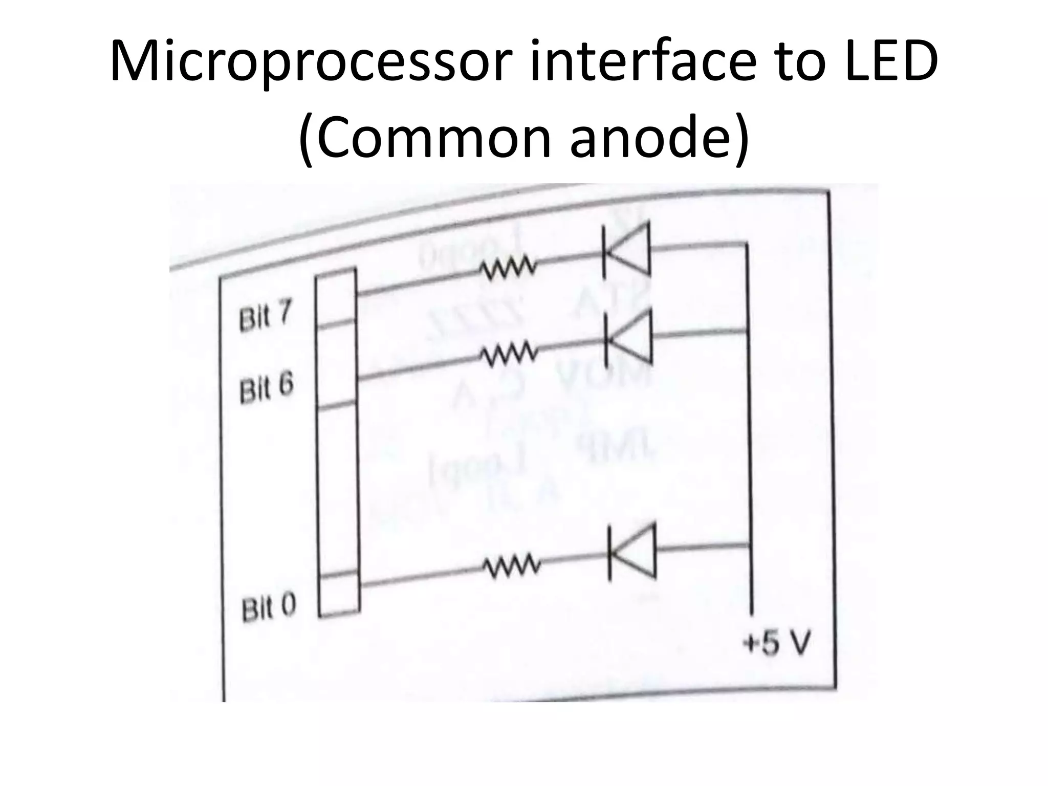
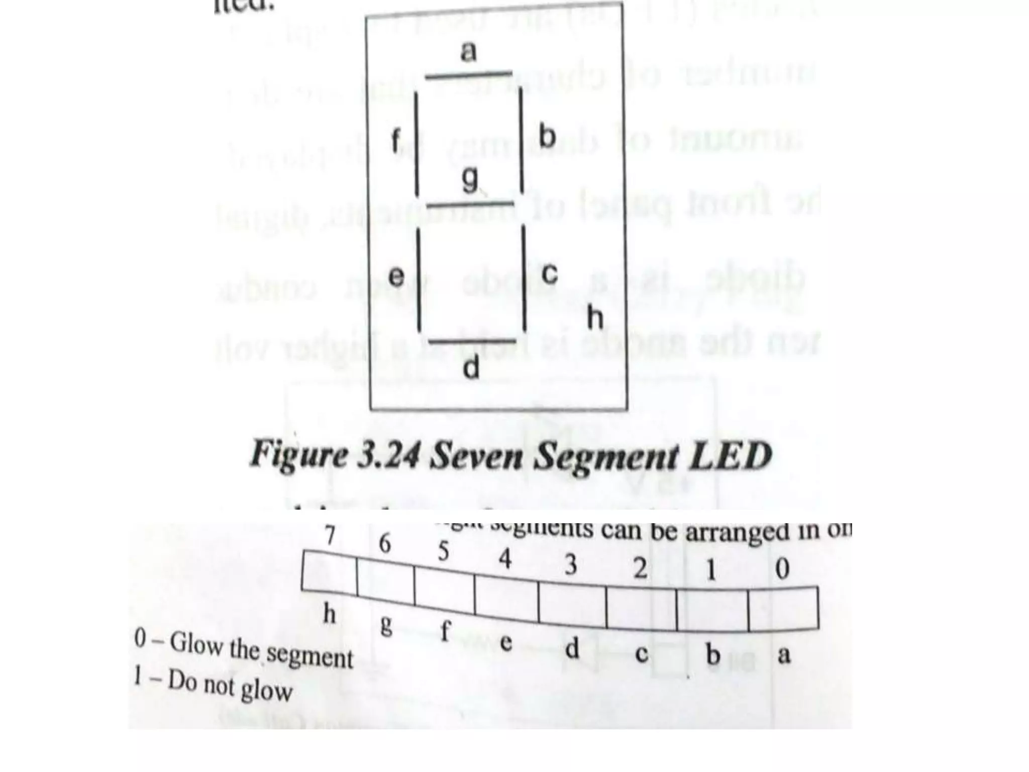
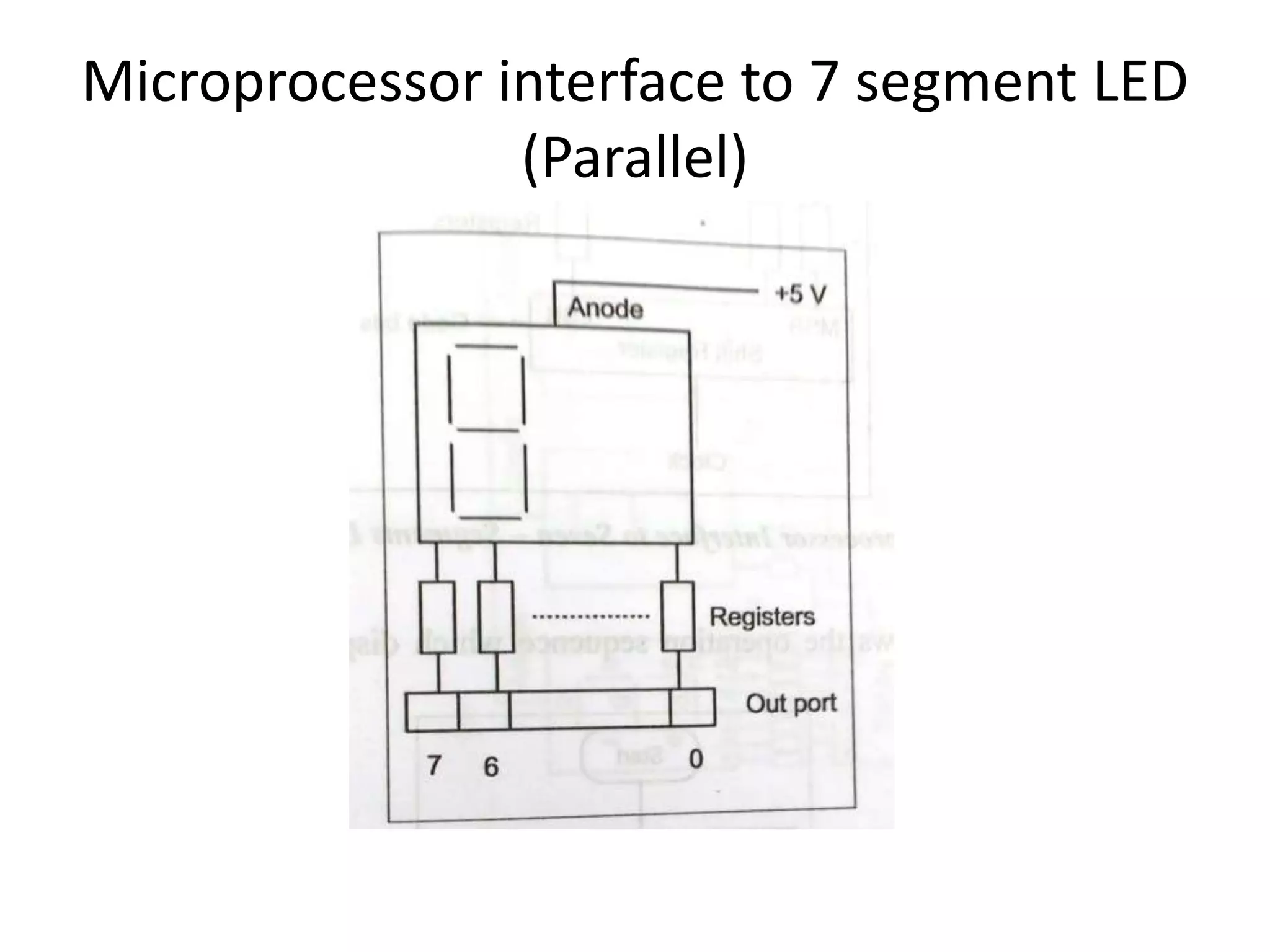
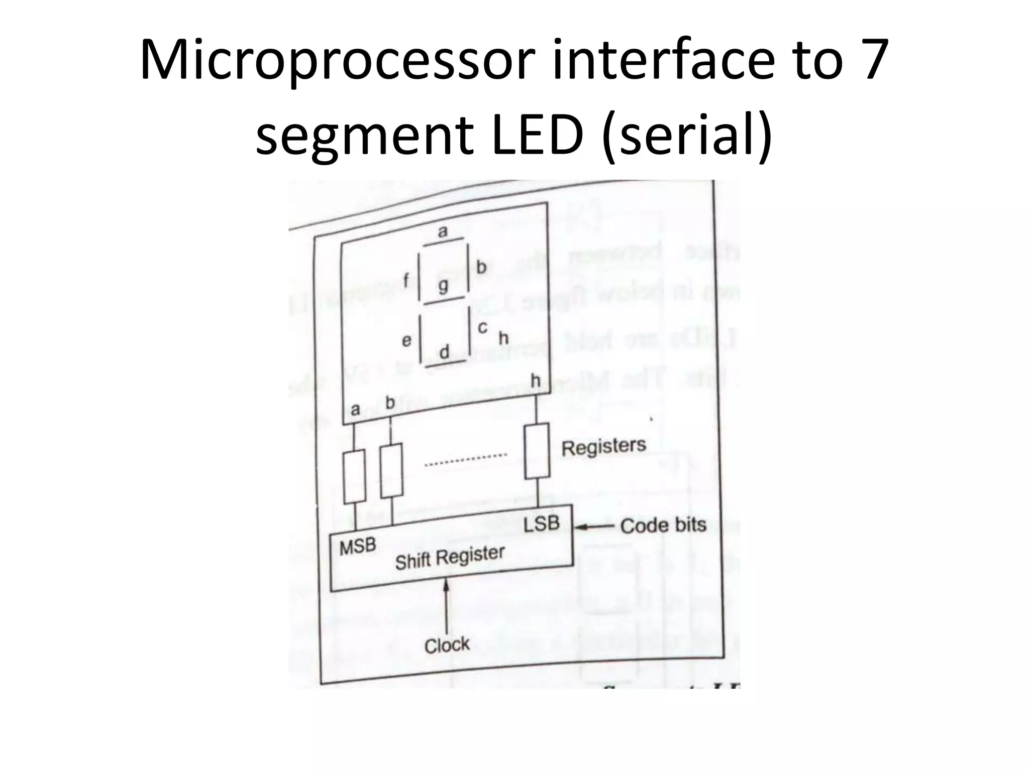
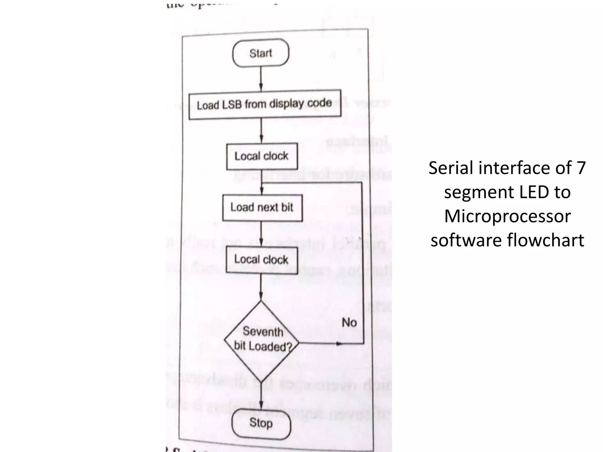
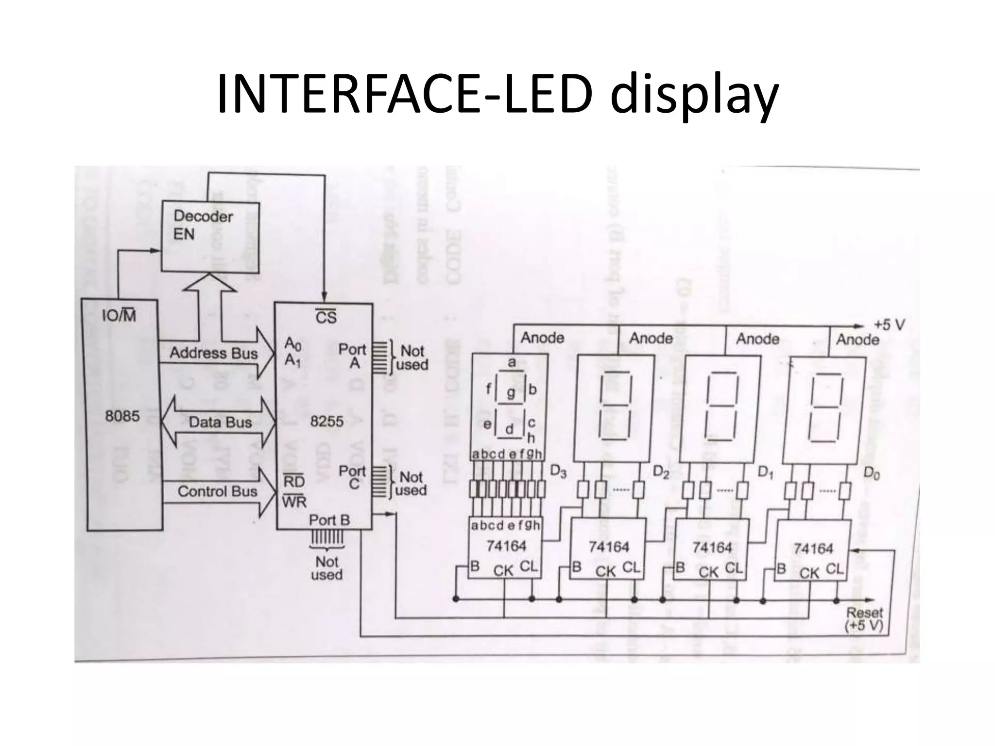
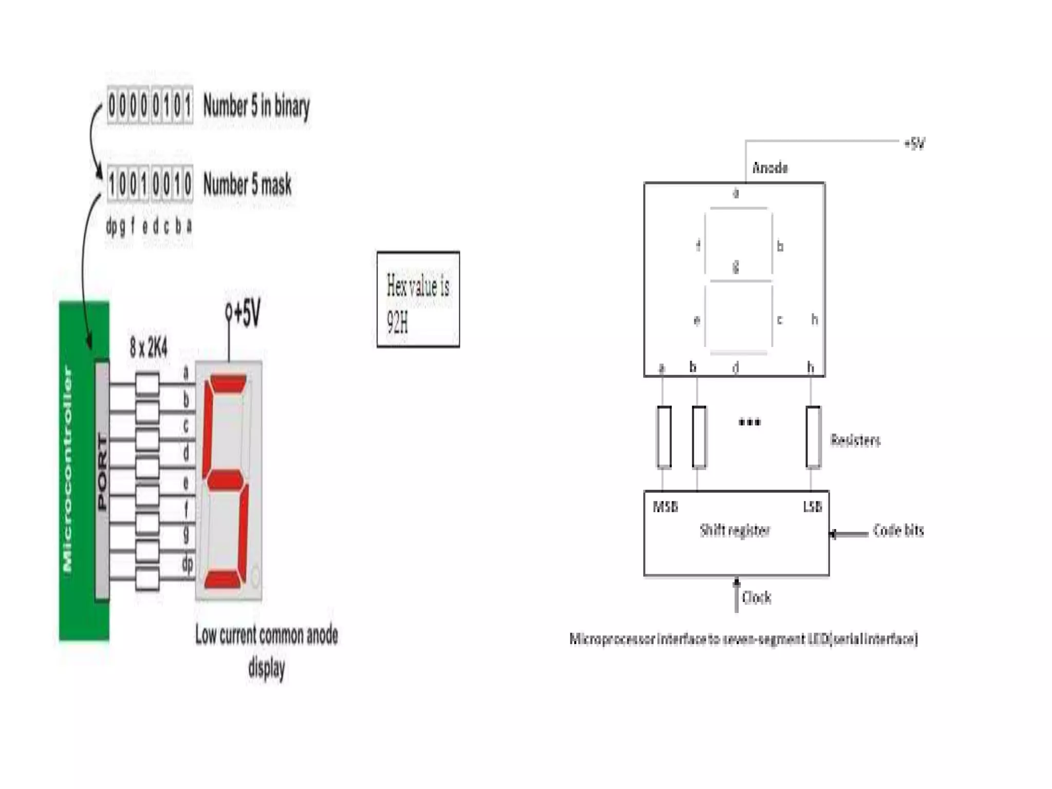
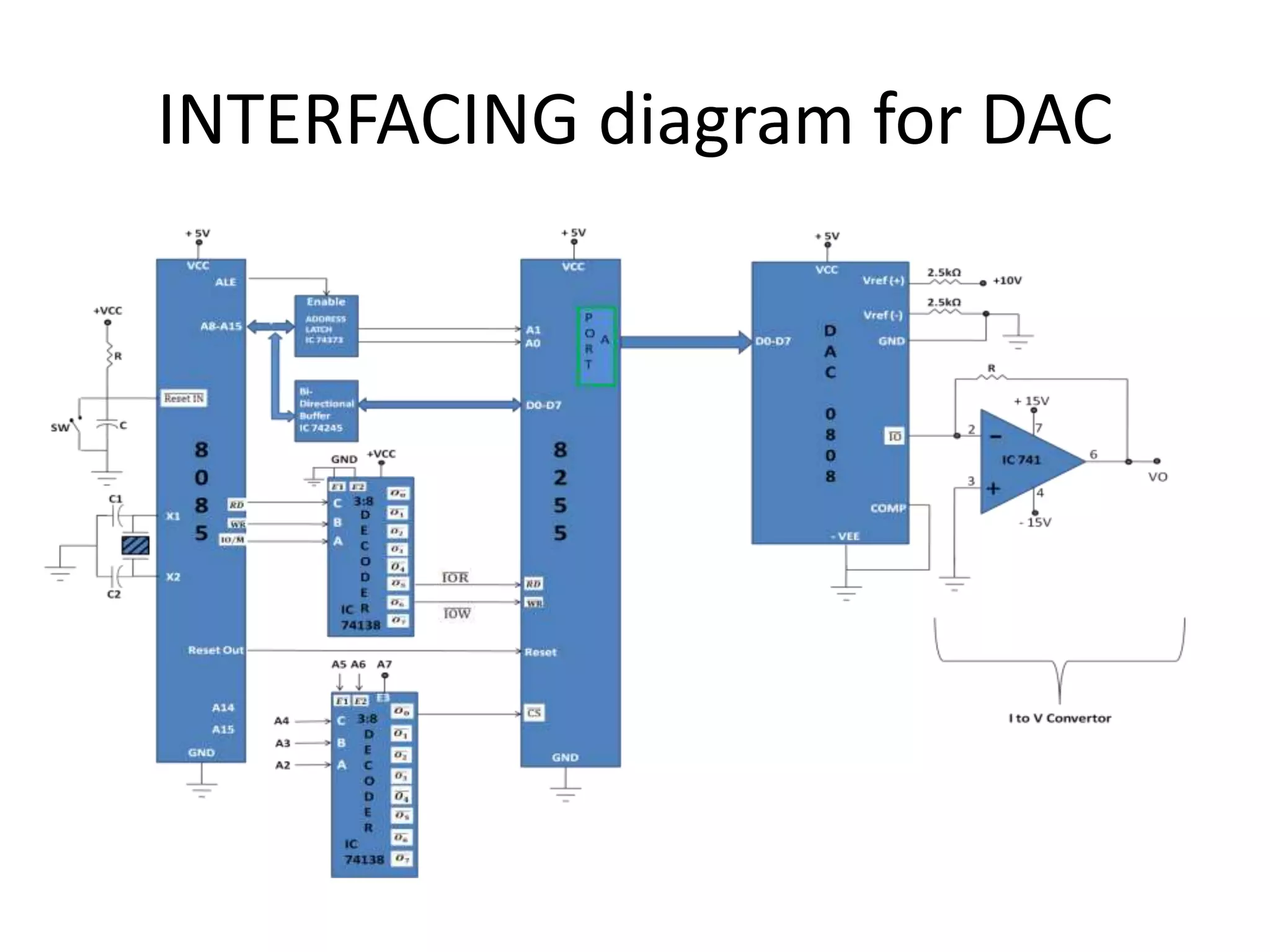
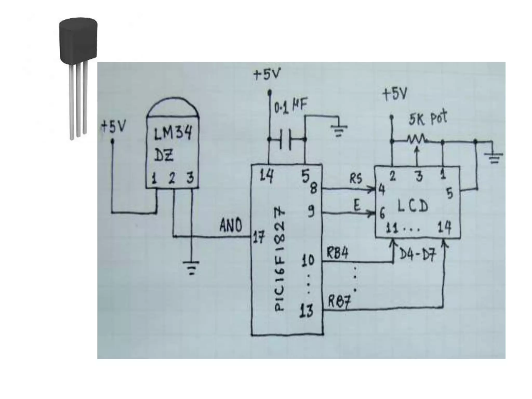
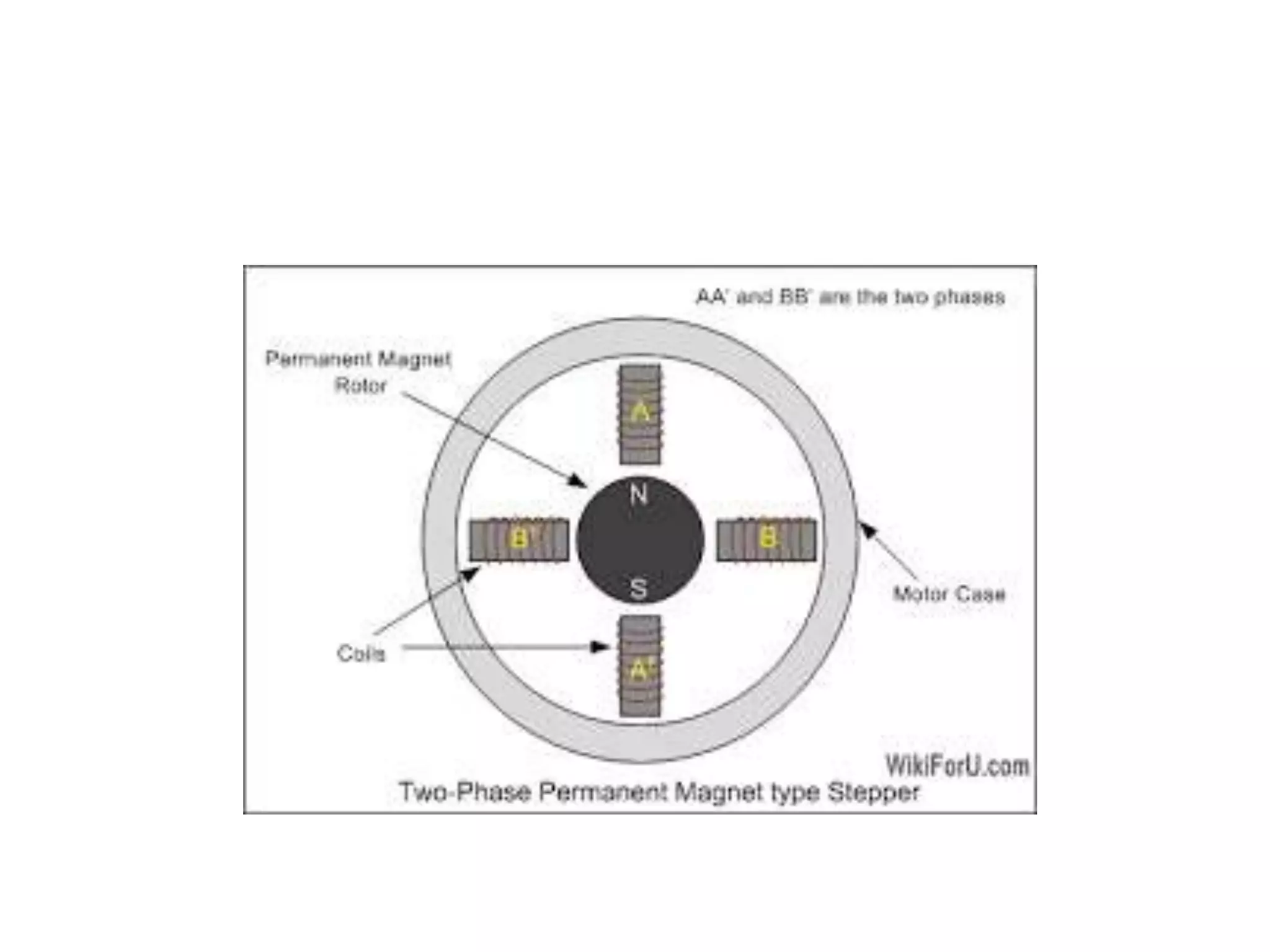
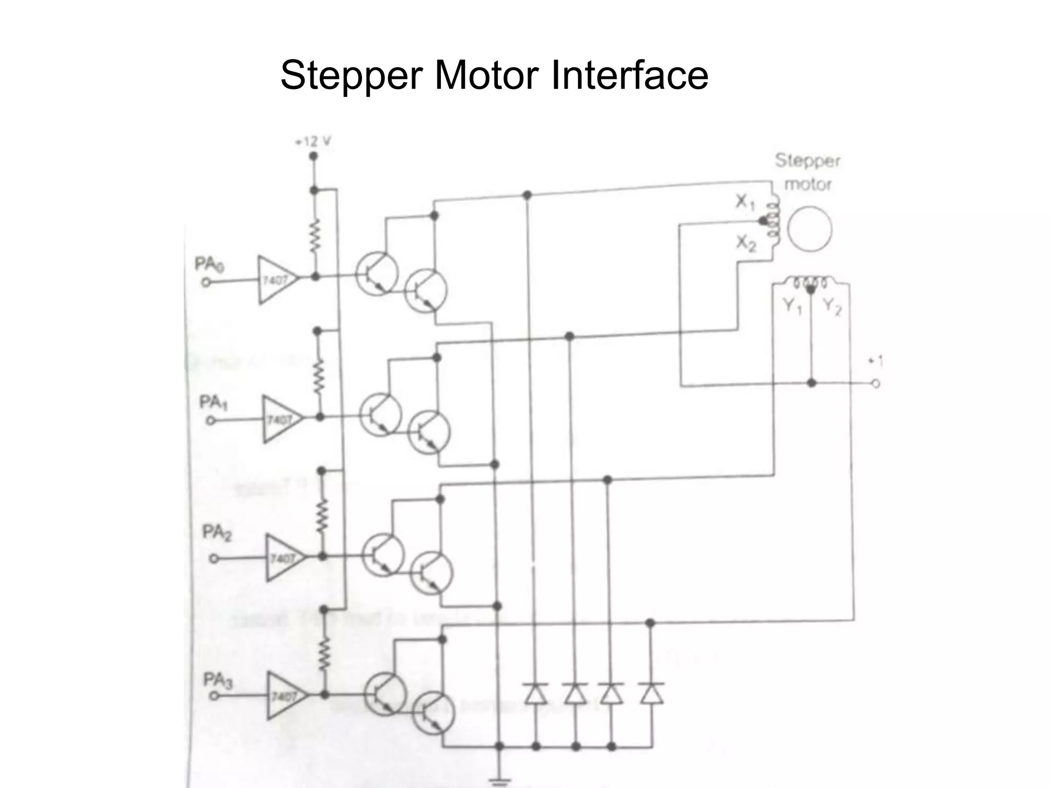
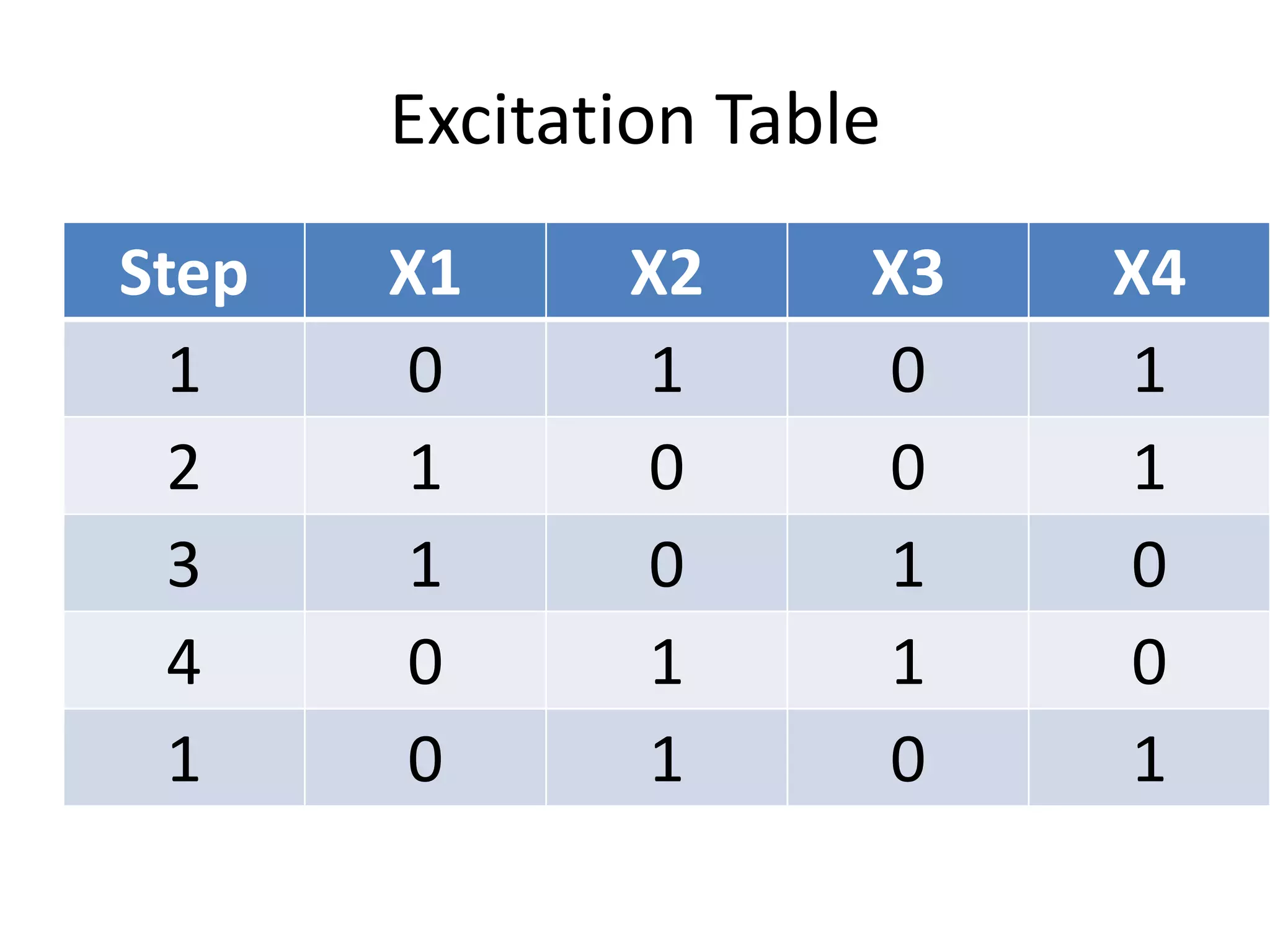
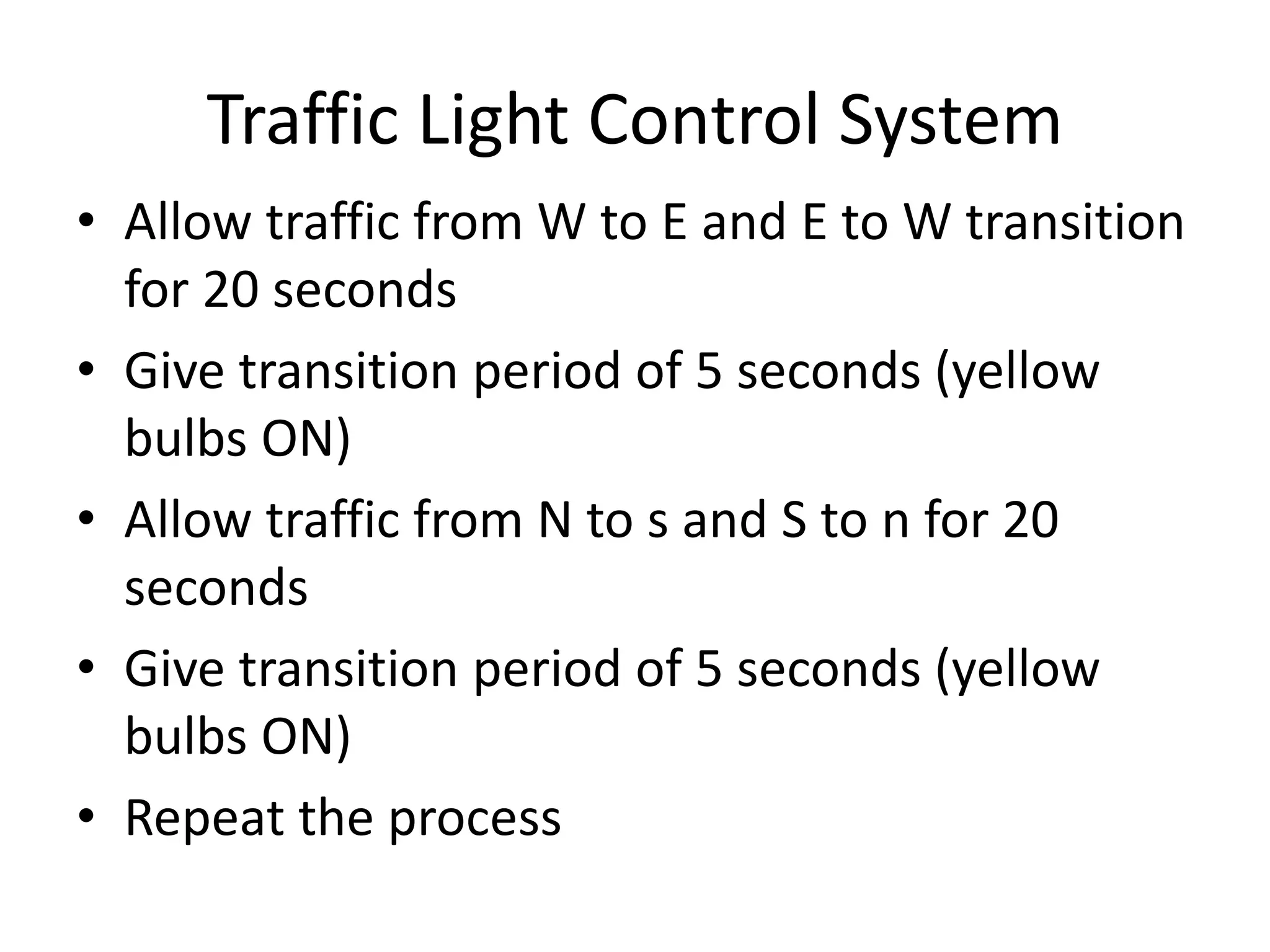
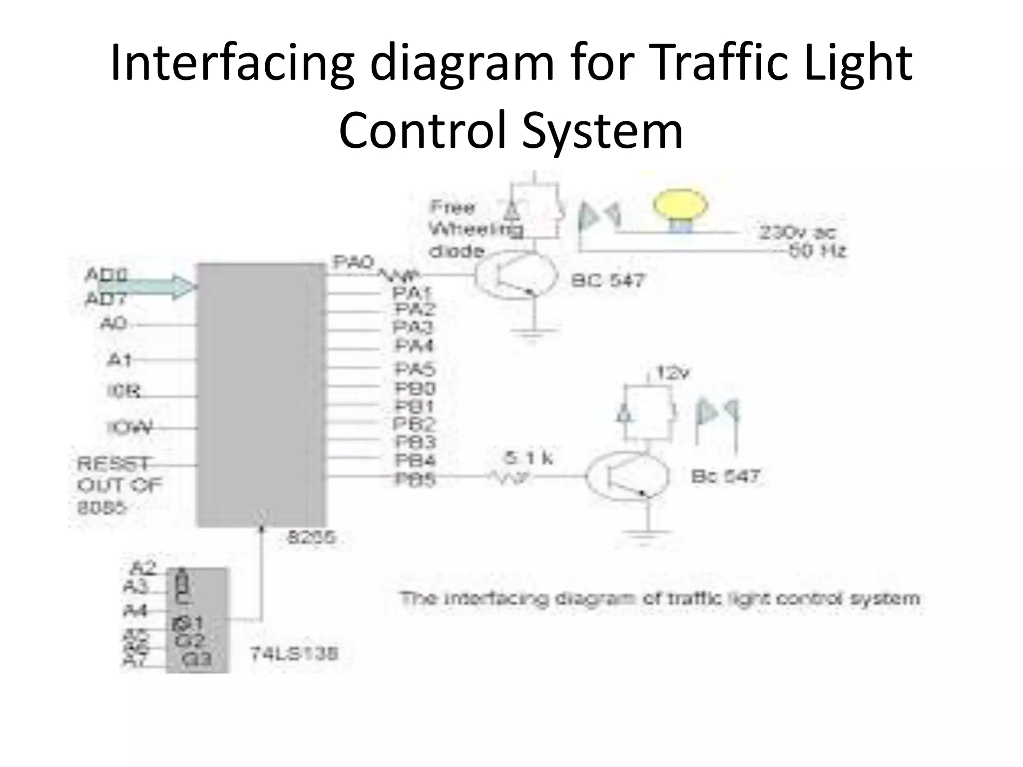
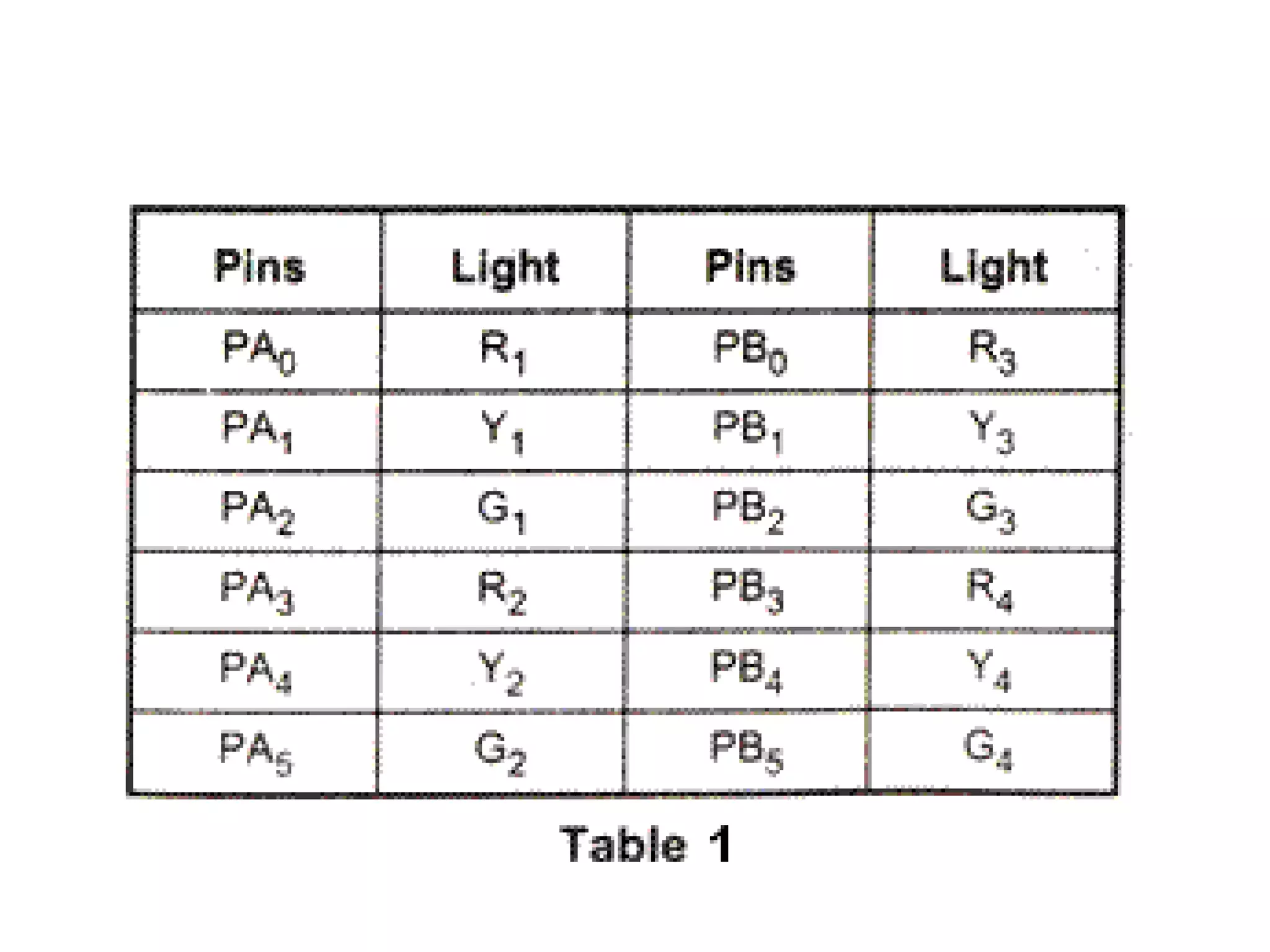
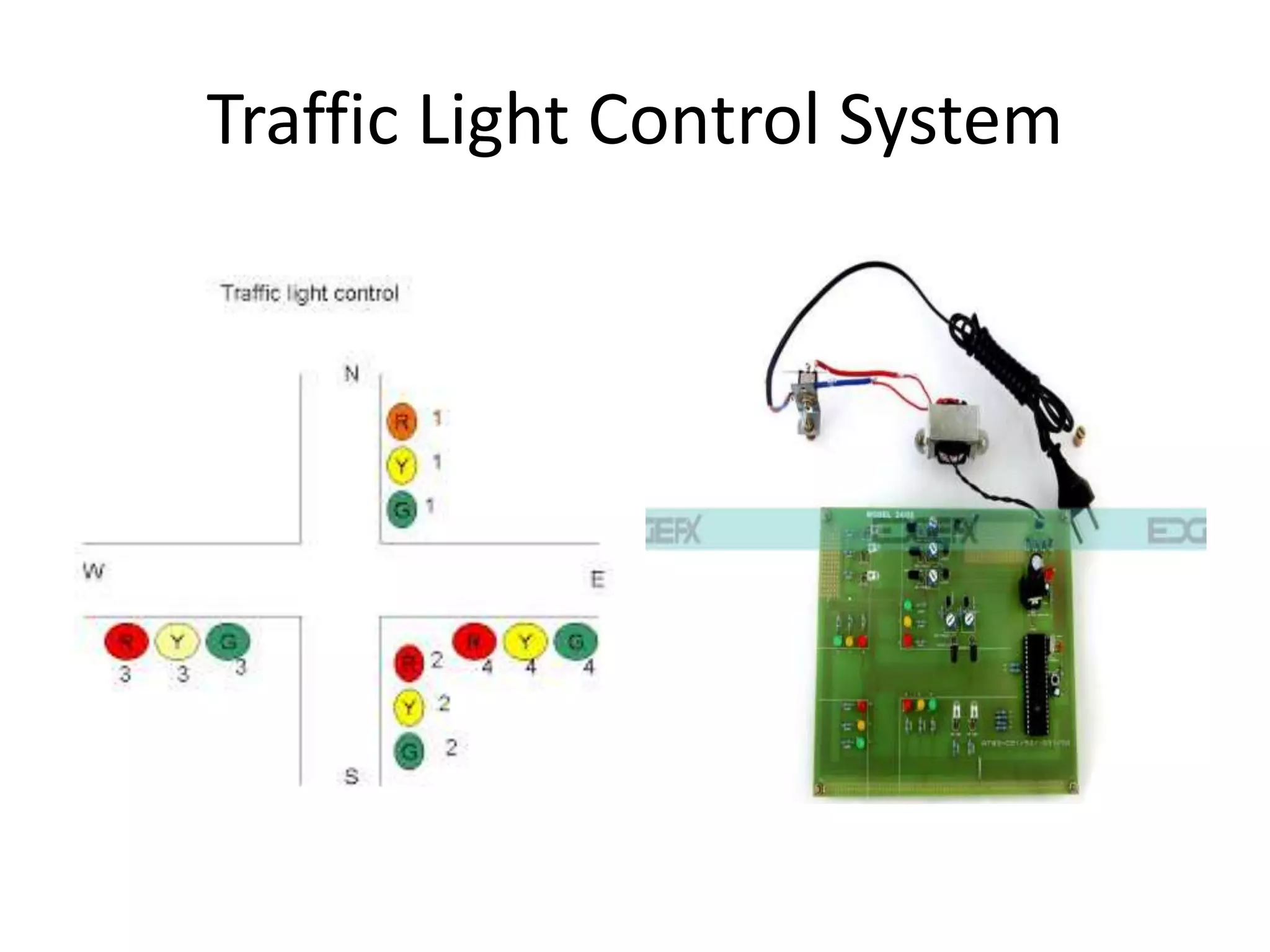
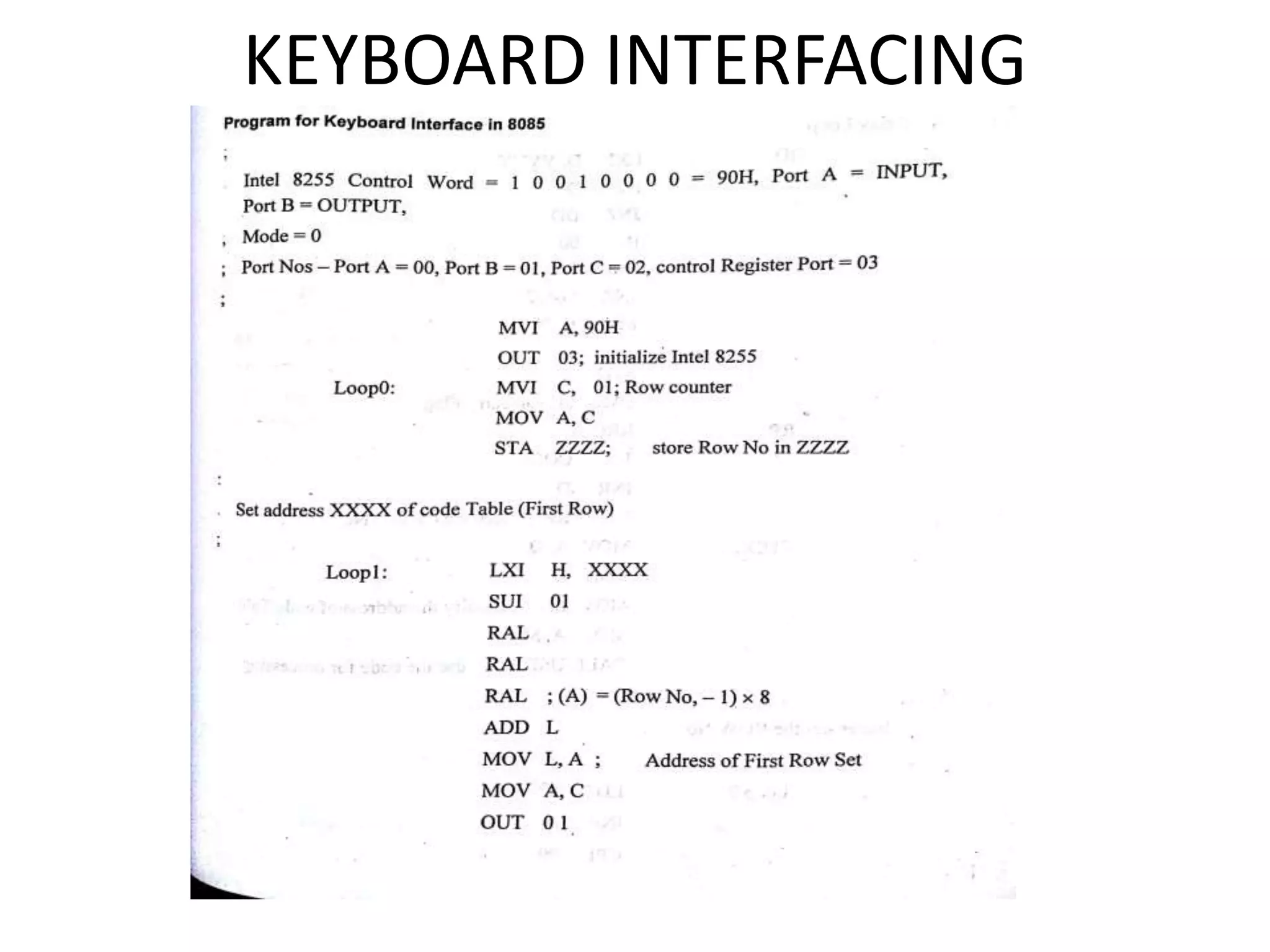
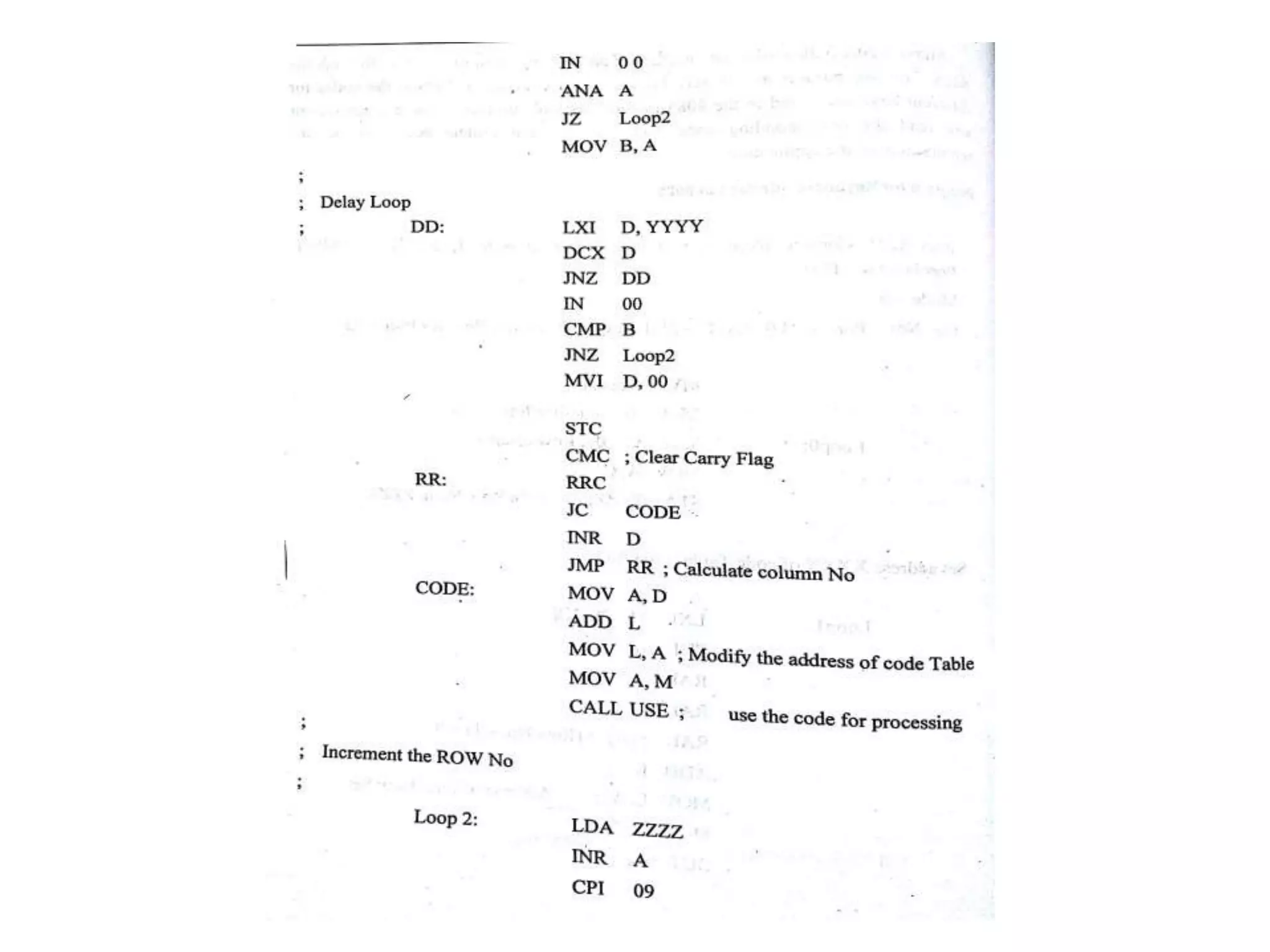
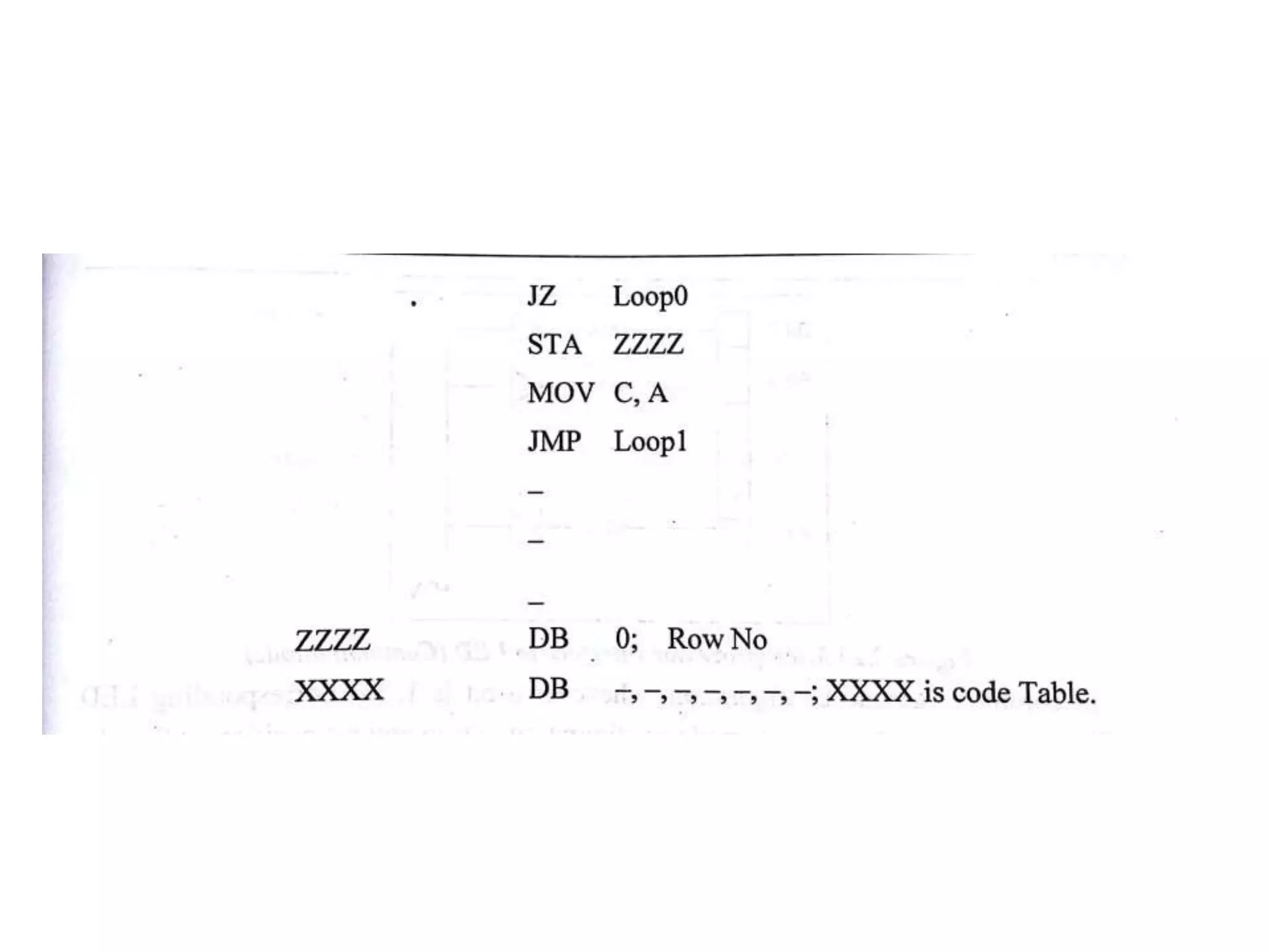
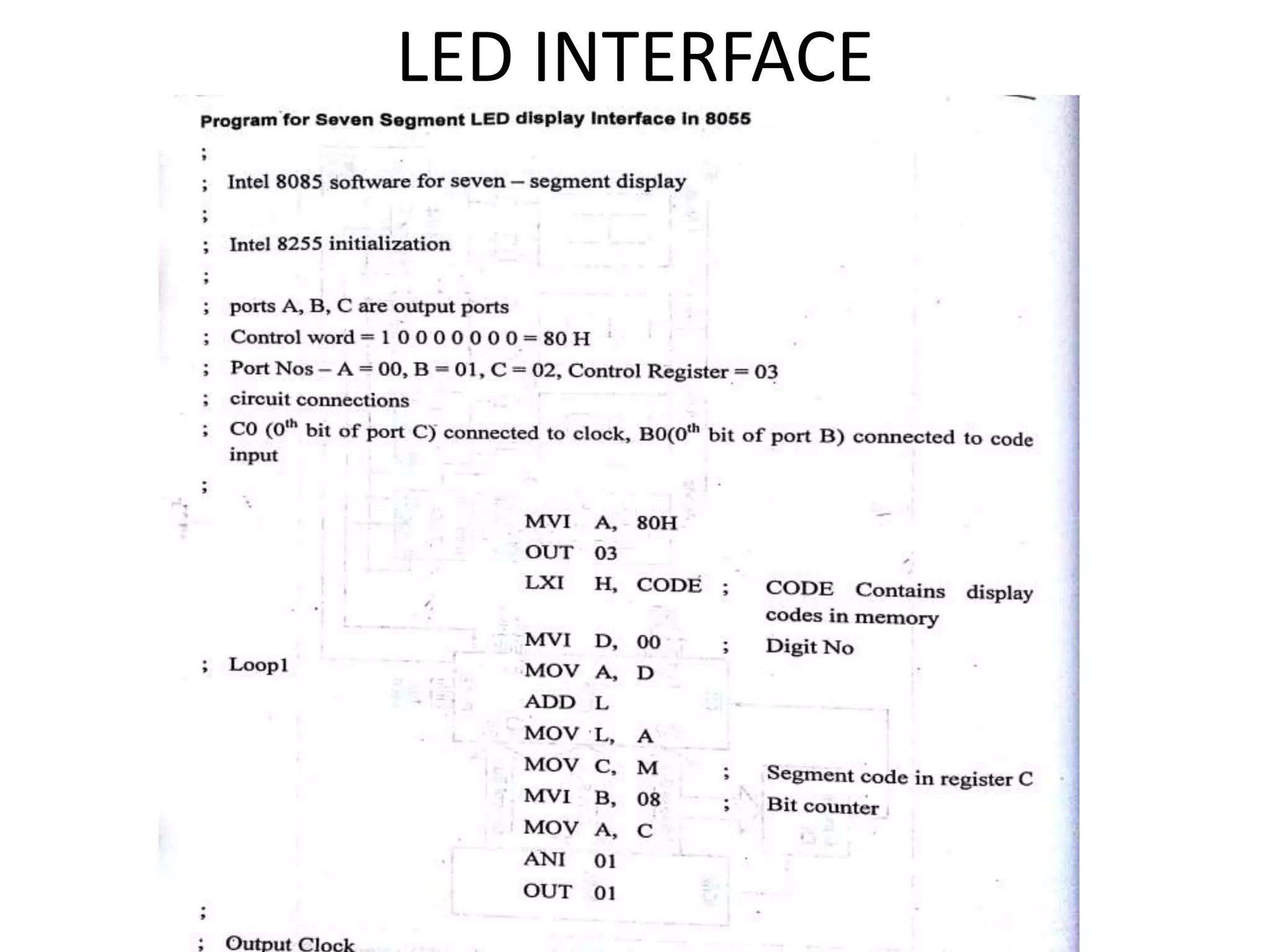
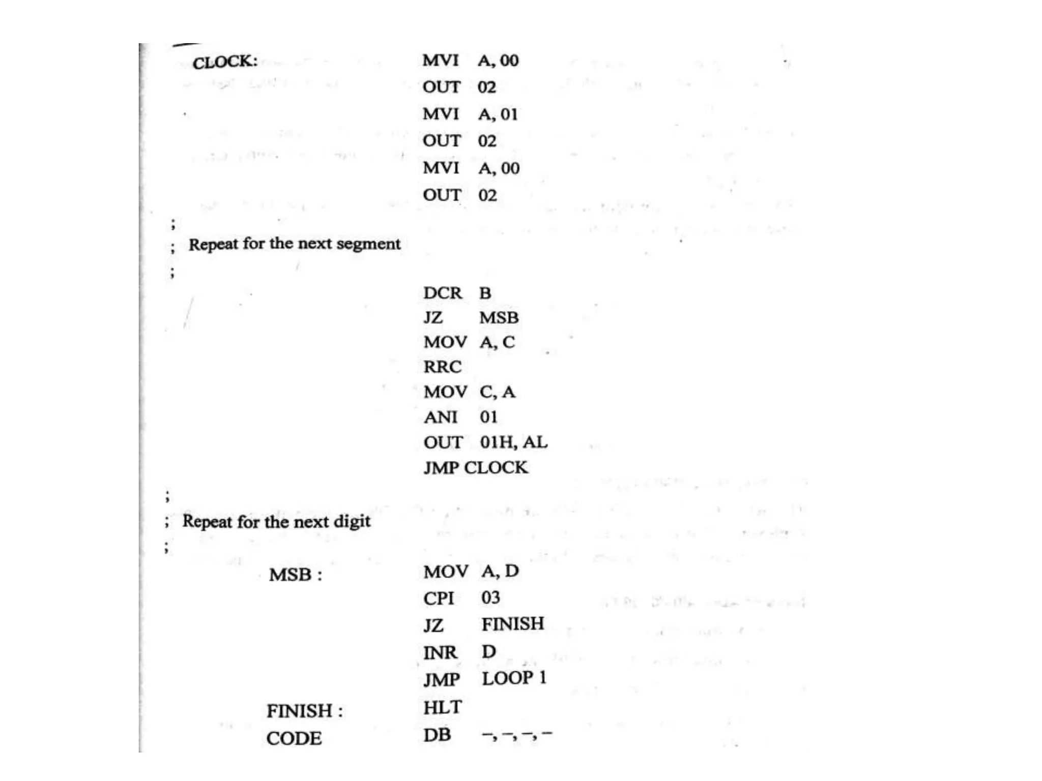
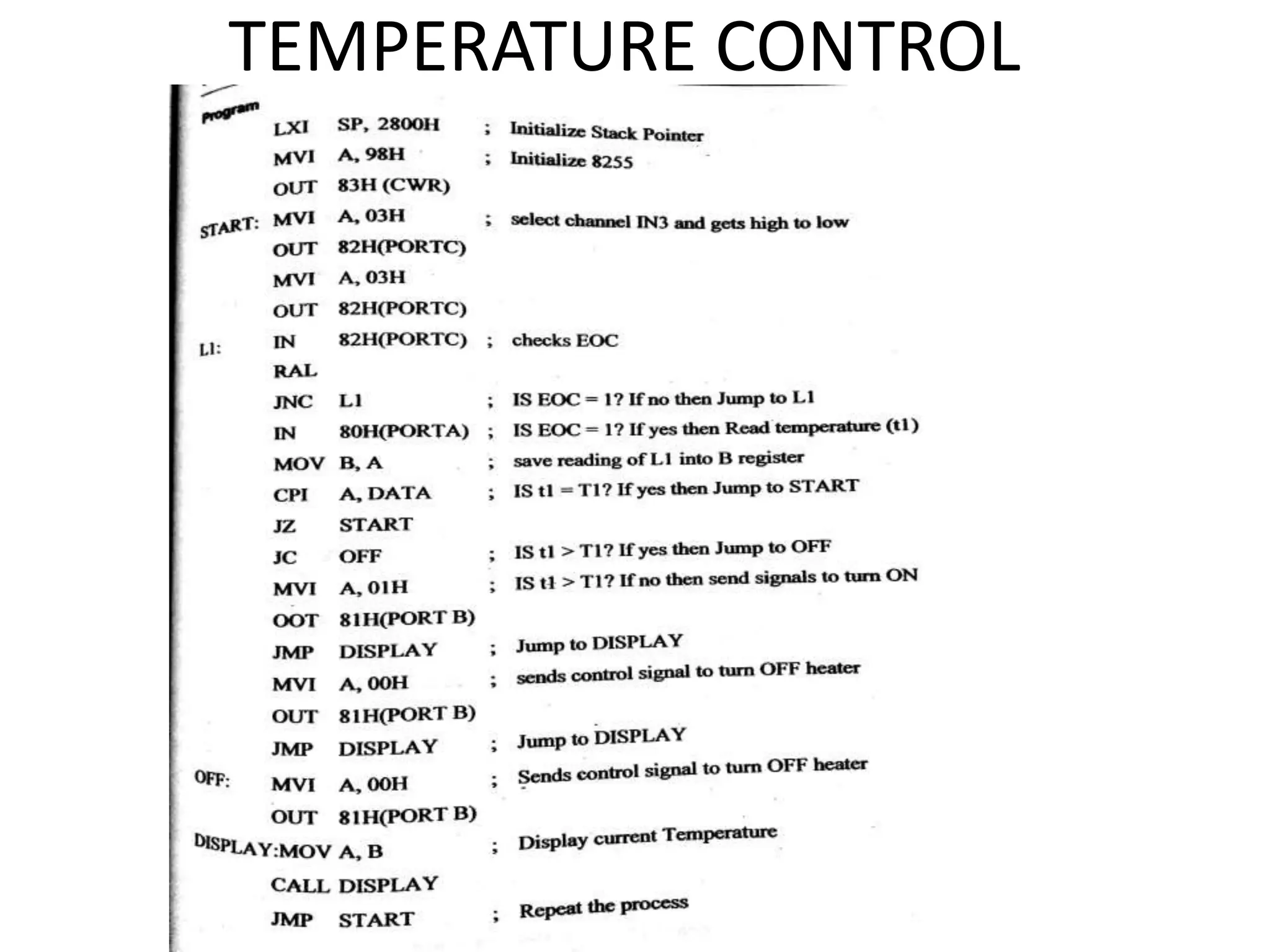
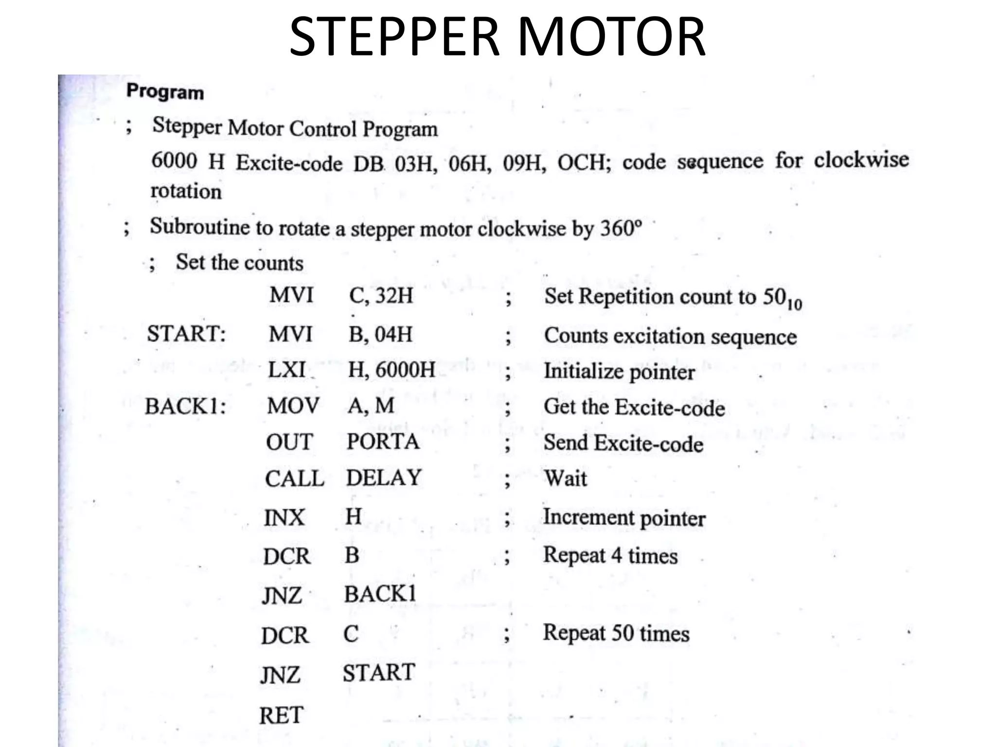
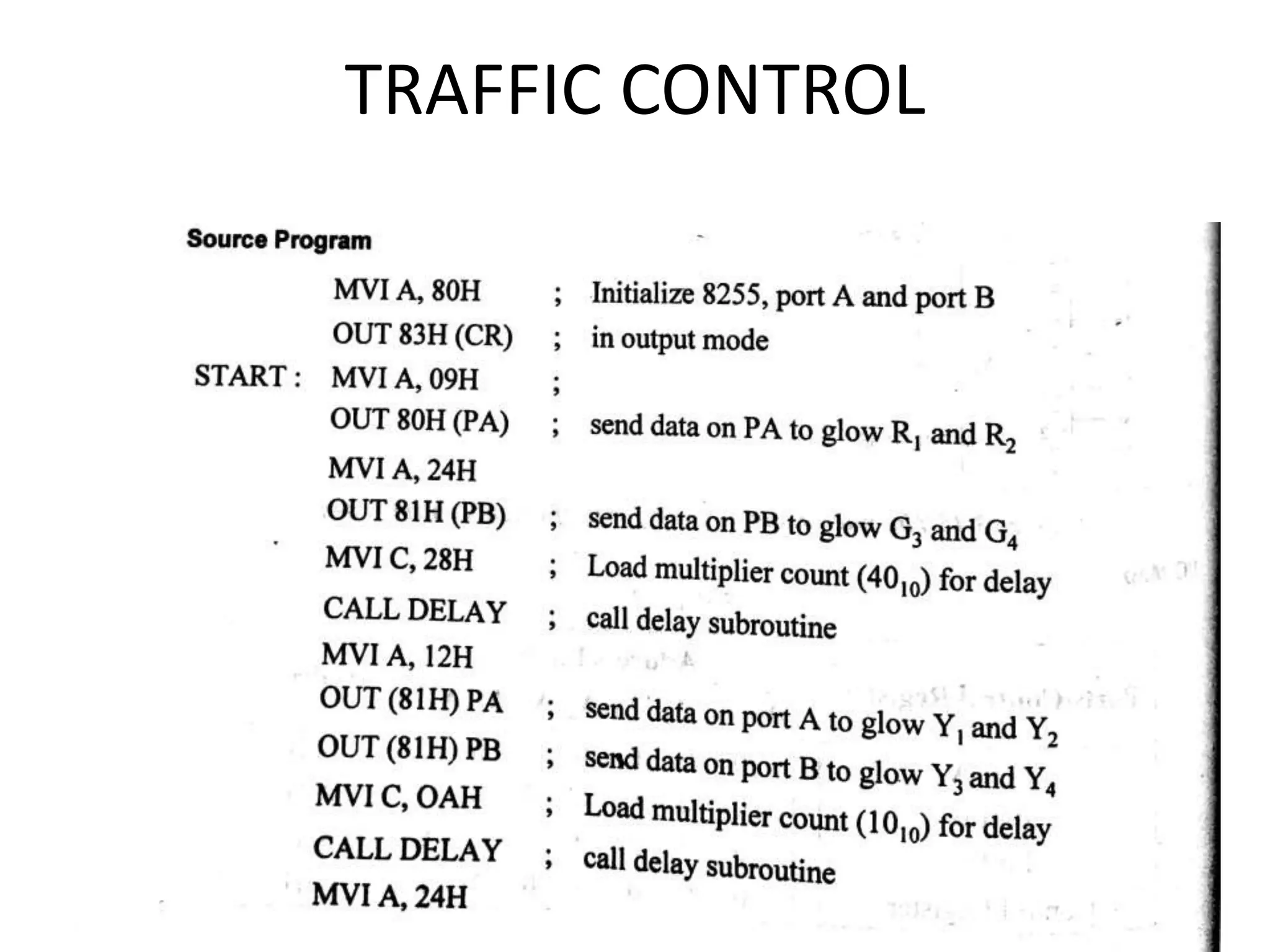
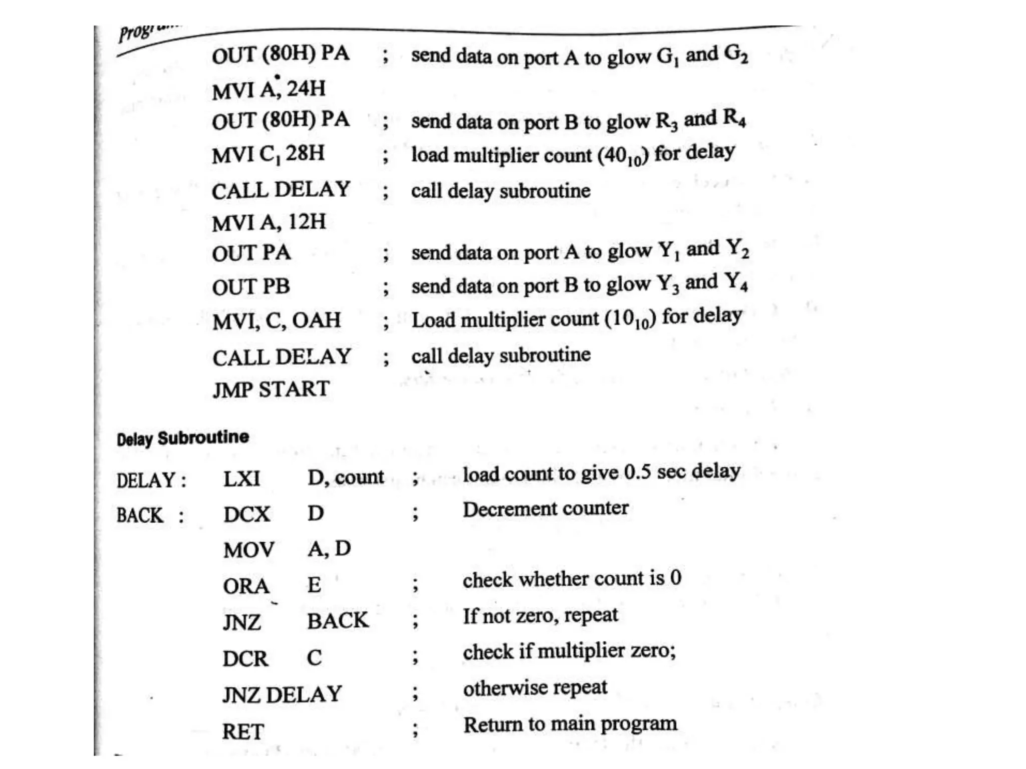
UNIT 3
PROGRAMMABLE PERIPERAL
INTERFACE
Content
• Introduction
• Architecture of 8255
• Keyboard interfacing
• LED display –interfacing
• ADC and DAC interface
• Temperature Control
• Stepper Motor Control
• Traffic Control interface
Introduction
• To communicate with the outside world,
microprocessor use peripherals (I/O devices)
• Input devices – Keyboards, A/D converters
etc.,
• Output devices – CRT, Printers, LEDs etc.,
• Peripherals are connected to the
microprocessors through electronic circuit
known as interfacing circuits.
Microprocessors unit with I/O devices
Input
devices
(keyboard)
Micro
processors
Output
devices
(LED)
Input
peripherals
Output
peripherals
• Some of the general purpose interfacing devices
– I/O ports
– Programmable peripherals interface (PPI)
– DMA controllers(Direct memory access)
– Interrupt controller
• Some of the special purpose interfacing devices
– CRT controller
– Keyboard
– Display
– Floppy Disc controllers
Some peripheral interfacing chips of
8085 and 8086 microprocessors.
• Programmable peripherals interface Inter 8255 (PPI)
• Programmable Interrupt controller (PIC) Intel 8259
• Programmable communication interface (PCI) Intel
8251
• Keyboard display Controller Intel 8279
• Programmable counter /Inverter timer Intel 8253
• A/D and D/A Converter Interfacing
Microprocessors unit with I/O devices
Input
devices
(key
board)
PPI
8255
Micro
proce
ssors
8279
Display
Output
device
(LED)
Peripheral
Interface
Display
Interface
Address Space Partitioning
• Two schemes for the allocation of addresses
to memories and I/O devices
– Memory mapped I/O
– I/O mapped I/O
Memory mapped I/O
• It has only one address space
• Address space is defined as the set of all
possible addresses that a microprocessor can
generate
• Some addresses assigned to memories and
Some addresses to I/O devices
• Memory locations are assigned with addresses
from 8000 to 84FF
• It is suitable for small system.
I/O mapped I/O scheme
• In this scheme, addresses assigned to
memories locations can also be assigned to
I/O devices
• When the signal is high, then address on the
address bus is for an I/O devices
• When the signal is low, then address on the
address bus is for memory locations.
I/O mapped I/O scheme
• Two extra instruction IN and OUT are used to
address I/O devices.
• The IN instruction is used to read the data of
an input devices.
• The OUT instruction is used to send the data
of an input devices.
• This scheme is suitable for a large system.
PROGRAMMABLE PERIPHERALS INTERFACE INTER 8255
(PPI)
Operating mode of 8255
• Bit Set Reset (BSR) Mode
• I/O Mode
Bit Set Reset (BSR) Mode
BSR control word format
I/O Mode
• The 8255 has the following 3 modes of
operation
– Mode 0 – Simple Input/output
– Mode 1 – Input / Output with the Handshake or
strobed
– Mode 2 – Bi-directional I/O
I/O Mode
Mode 0 – Simple Input/output
– Port A and port B are used as two simple 8-bit I/O
port
– Port C as two 4-bit port
• Features
– Outputs are latched
– Inputs are buffered not latched
– Ports do not have handshake or interrupt
capability
I/O Mode
• Mode 1 – Input / Output with the Handshake
– Input or output data transfer is controlled by
handshaking signals.
– Handshaking signals are used to transfer data
between devices whose data transfer speeds are
not same.
– Port A and Port B are designed to operate with the
Port C.
– When Port A and Port B are programmed in Mode
1, 6 pins of port C is used for their control.
I/O Mode
• D0-D7 data bus
– bi directional, tri state data bus line
– It is used to transfer data and control word from
8085 to 8255
• RD (Read)
– When this pin is low, the CPU can read data in the
port or status word through the data buffer
• WR (write)
– When this pin is low, the CPU can write data in the
port or in the control register through the data
buffer
I/O Mode
• Mode 2 – Bi-directional I/O
• Port A can be programmed to operate as a
bidirectional port.
• The mode 2 operation is only for port A
• When port A is programmed in Mode 2, the
Port B can be used in either Mode 1 or Mode
0.
• Mode 2 operation the port a is controlled by
PC3 to PC7 of port C.
PIN
DIAGRAM
OF 8255
PROGRAMMING and OPERATION of
8255
• Programming in MODE 0
• D7 –set to 1
• D6,D5,D2- all set to 0 –MODE 0
• D4,D3,D1 and D0- determine weather the
corresponding ports are to configured as input
or output
A B GROUP A GROUP B
D4 D3 D1 D0 PORT A PORTC U PORT B PORT C L
0 0 0 0 OUT OUT OUT OUT
0 0 0 1 OUT OUT OUT IP
0 0 1 0 OUT OUT IP OUT
0 0 1 1 OUT OUT IP IP
0 1 0 0 OUT IP OUT OUT
0 1 0 1 OUT IP OUT IP
0 1 1 0 OUT IP IP OUT
0 1 1 1 OUT IP IP IP
1 0 0 0 IP OUT OUT OUT
1 0 0 1 IP OUT OUT IP
1 0 1 0 IP OUT IP OUT
1 0 1 1 IP OUT IP IP
1 1 0 0 IP IP OUT OUT
1 1 0 1 IP IP OUT IP
1 1 1 0 IP IP IP OUT
1 1 1 1 IP IP IP IP
Programming in MODE 1
• IBF- input buffer full
• INTR- interrupt request
• INTE-interrupt enable
• OBF-output buffer full
• INTR-interrupt request
• INTE-interrupt enable
Programming in MODE 2
Interfacing cable
Basic Key operation
2 X 2 Key operation
Keyboard Microprocessor Interface software Flowchart
INTERFACING-keyboard
LED Operation
Microprocessor interface to LED
(Common anode)
Microprocessor interface to 7 segment LED
(Parallel)
Microprocessor interface to 7
segment LED (serial)
Serial interface of 7
segment LED to
Microprocessor
software flowchart
INTERFACE-LED display
ADC INTERFACE
BLOCK diagram of ADC 0808
PIN diagram of ADC 0808
DAC INTERFACE
Pin diagram of DAC
Pin diagram of DAC
INTERFACING diagram for DAC
TEMPERATURE CONTROL
• Temperature sensor –convert temp to
electrical signal by thermistor
• Transducer convert physical data into
electrical signal
• Physical data –temp, light, flow, speed etc…
• LM34 & LM35 –temperature sensor by
NATIONAL SEMICONDUCTOR CO-OPERATION
• LM34
• Output voltage is
linearly proportional to
Fahrenheit temp
• No external calibration
• 10mV for each degree
of Fahrenheit temp
• LM35
• Output voltage is
linearly proportional to
Celsius temp
• No external calibration
• 10mV for each degree
of Centigrate temp
STEPPER MOTOR CONTROL interface
• Digital motor used to translate electrical pulse
into mechanical movement
• Center tap winding connected to 12 V supply
• Motor can be excited by grounding four
terminals of the two windings
• ROTOR-Stepper motor has permanent magnet
rotor .It is also known as shaft
• STEP ANGLE-It is minimum degree of rotation
associated with a single step
Stepper Motor Interface
Excitation Table
Step X1 X2 X3 X4
1 0 1 0 1
2 1 0 0 1
3 1 0 1 0
4 0 1 1 0
1 0 1 0 1
Traffic Light Control System
• Allow traffic from W to E and E to W transition
for 20 seconds
• Give transition period of 5 seconds (yellow
bulbs ON)
• Allow traffic from N to s and S to n for 20
seconds
• Give transition period of 5 seconds (yellow
bulbs ON)
• Repeat the process
Traffic Light Control System
Interfacing diagram for Traffic Light
Control System
Traffic Light Control System
KEYBOARD INTERFACING
LED INTERFACE
TEMPERATURE CONTROL
STEPPER MOTOR
TRAFFIC CONTROL
UNIT III PROGRAMMABLE PERIPHERAL INTERFACE

UNIT III PROGRAMMABLE PERIPHERAL INTERFACE

  • 1.
  • 2.
    Content • Introduction • Architectureof 8255 • Keyboard interfacing • LED display –interfacing • ADC and DAC interface • Temperature Control • Stepper Motor Control • Traffic Control interface
  • 3.
    Introduction • To communicatewith the outside world, microprocessor use peripherals (I/O devices) • Input devices – Keyboards, A/D converters etc., • Output devices – CRT, Printers, LEDs etc., • Peripherals are connected to the microprocessors through electronic circuit known as interfacing circuits.
  • 4.
    Microprocessors unit withI/O devices Input devices (keyboard) Micro processors Output devices (LED) Input peripherals Output peripherals
  • 5.
    • Some ofthe general purpose interfacing devices – I/O ports – Programmable peripherals interface (PPI) – DMA controllers(Direct memory access) – Interrupt controller • Some of the special purpose interfacing devices – CRT controller – Keyboard – Display – Floppy Disc controllers
  • 6.
    Some peripheral interfacingchips of 8085 and 8086 microprocessors. • Programmable peripherals interface Inter 8255 (PPI) • Programmable Interrupt controller (PIC) Intel 8259 • Programmable communication interface (PCI) Intel 8251 • Keyboard display Controller Intel 8279 • Programmable counter /Inverter timer Intel 8253 • A/D and D/A Converter Interfacing
  • 7.
    Microprocessors unit withI/O devices Input devices (key board) PPI 8255 Micro proce ssors 8279 Display Output device (LED) Peripheral Interface Display Interface
  • 8.
    Address Space Partitioning •Two schemes for the allocation of addresses to memories and I/O devices – Memory mapped I/O – I/O mapped I/O
  • 9.
    Memory mapped I/O •It has only one address space • Address space is defined as the set of all possible addresses that a microprocessor can generate • Some addresses assigned to memories and Some addresses to I/O devices • Memory locations are assigned with addresses from 8000 to 84FF • It is suitable for small system.
  • 10.
    I/O mapped I/Oscheme • In this scheme, addresses assigned to memories locations can also be assigned to I/O devices • When the signal is high, then address on the address bus is for an I/O devices • When the signal is low, then address on the address bus is for memory locations.
  • 11.
    I/O mapped I/Oscheme • Two extra instruction IN and OUT are used to address I/O devices. • The IN instruction is used to read the data of an input devices. • The OUT instruction is used to send the data of an input devices. • This scheme is suitable for a large system.
  • 12.
  • 13.
    Operating mode of8255 • Bit Set Reset (BSR) Mode • I/O Mode
  • 14.
    Bit Set Reset(BSR) Mode BSR control word format
  • 15.
    I/O Mode • The8255 has the following 3 modes of operation – Mode 0 – Simple Input/output – Mode 1 – Input / Output with the Handshake or strobed – Mode 2 – Bi-directional I/O
  • 16.
    I/O Mode Mode 0– Simple Input/output – Port A and port B are used as two simple 8-bit I/O port – Port C as two 4-bit port • Features – Outputs are latched – Inputs are buffered not latched – Ports do not have handshake or interrupt capability
  • 17.
    I/O Mode • Mode1 – Input / Output with the Handshake – Input or output data transfer is controlled by handshaking signals. – Handshaking signals are used to transfer data between devices whose data transfer speeds are not same. – Port A and Port B are designed to operate with the Port C. – When Port A and Port B are programmed in Mode 1, 6 pins of port C is used for their control.
  • 18.
    I/O Mode • D0-D7data bus – bi directional, tri state data bus line – It is used to transfer data and control word from 8085 to 8255 • RD (Read) – When this pin is low, the CPU can read data in the port or status word through the data buffer • WR (write) – When this pin is low, the CPU can write data in the port or in the control register through the data buffer
  • 19.
    I/O Mode • Mode2 – Bi-directional I/O • Port A can be programmed to operate as a bidirectional port. • The mode 2 operation is only for port A • When port A is programmed in Mode 2, the Port B can be used in either Mode 1 or Mode 0. • Mode 2 operation the port a is controlled by PC3 to PC7 of port C.
  • 20.
  • 22.
    PROGRAMMING and OPERATIONof 8255 • Programming in MODE 0 • D7 –set to 1 • D6,D5,D2- all set to 0 –MODE 0 • D4,D3,D1 and D0- determine weather the corresponding ports are to configured as input or output
  • 23.
    A B GROUPA GROUP B D4 D3 D1 D0 PORT A PORTC U PORT B PORT C L 0 0 0 0 OUT OUT OUT OUT 0 0 0 1 OUT OUT OUT IP 0 0 1 0 OUT OUT IP OUT 0 0 1 1 OUT OUT IP IP 0 1 0 0 OUT IP OUT OUT 0 1 0 1 OUT IP OUT IP 0 1 1 0 OUT IP IP OUT 0 1 1 1 OUT IP IP IP 1 0 0 0 IP OUT OUT OUT 1 0 0 1 IP OUT OUT IP 1 0 1 0 IP OUT IP OUT 1 0 1 1 IP OUT IP IP 1 1 0 0 IP IP OUT OUT 1 1 0 1 IP IP OUT IP 1 1 1 0 IP IP IP OUT 1 1 1 1 IP IP IP IP
  • 24.
  • 25.
    • IBF- inputbuffer full • INTR- interrupt request • INTE-interrupt enable • OBF-output buffer full • INTR-interrupt request • INTE-interrupt enable
  • 26.
  • 28.
  • 29.
  • 31.
    2 X 2Key operation
  • 32.
  • 33.
  • 36.
  • 38.
    Microprocessor interface toLED (Common anode)
  • 40.
    Microprocessor interface to7 segment LED (Parallel)
  • 41.
    Microprocessor interface to7 segment LED (serial)
  • 42.
    Serial interface of7 segment LED to Microprocessor software flowchart
  • 43.
  • 45.
  • 46.
  • 48.
  • 49.
  • 50.
  • 51.
  • 52.
  • 53.
    TEMPERATURE CONTROL • Temperaturesensor –convert temp to electrical signal by thermistor • Transducer convert physical data into electrical signal • Physical data –temp, light, flow, speed etc… • LM34 & LM35 –temperature sensor by NATIONAL SEMICONDUCTOR CO-OPERATION
  • 54.
    • LM34 • Outputvoltage is linearly proportional to Fahrenheit temp • No external calibration • 10mV for each degree of Fahrenheit temp • LM35 • Output voltage is linearly proportional to Celsius temp • No external calibration • 10mV for each degree of Centigrate temp
  • 56.
    STEPPER MOTOR CONTROLinterface • Digital motor used to translate electrical pulse into mechanical movement • Center tap winding connected to 12 V supply • Motor can be excited by grounding four terminals of the two windings • ROTOR-Stepper motor has permanent magnet rotor .It is also known as shaft • STEP ANGLE-It is minimum degree of rotation associated with a single step
  • 58.
  • 59.
    Excitation Table Step X1X2 X3 X4 1 0 1 0 1 2 1 0 0 1 3 1 0 1 0 4 0 1 1 0 1 0 1 0 1
  • 60.
    Traffic Light ControlSystem • Allow traffic from W to E and E to W transition for 20 seconds • Give transition period of 5 seconds (yellow bulbs ON) • Allow traffic from N to s and S to n for 20 seconds • Give transition period of 5 seconds (yellow bulbs ON) • Repeat the process
  • 61.
  • 62.
    Interfacing diagram forTraffic Light Control System
  • 64.
  • 65.
  • 68.
  • 70.
  • 71.
  • 72.