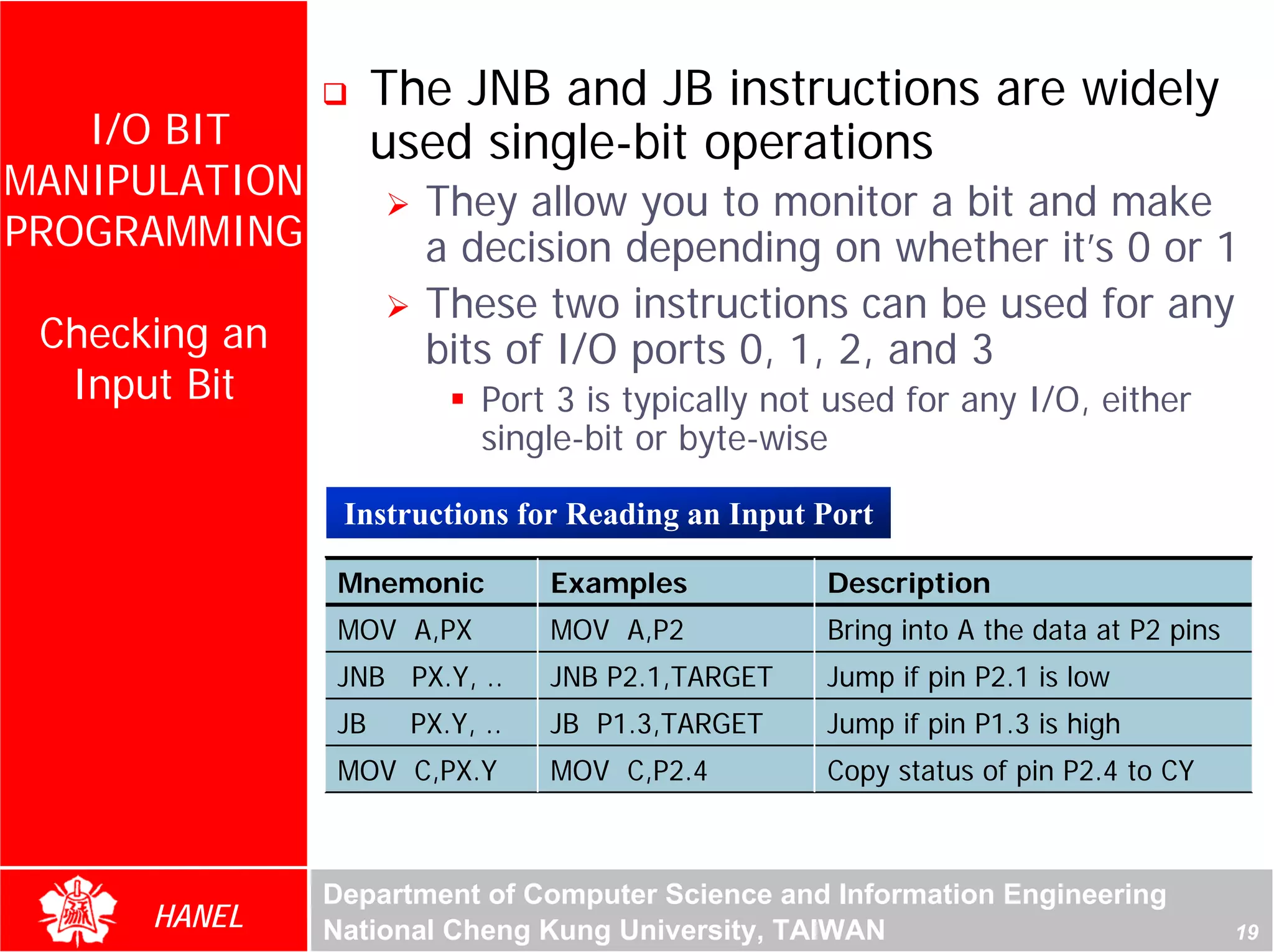
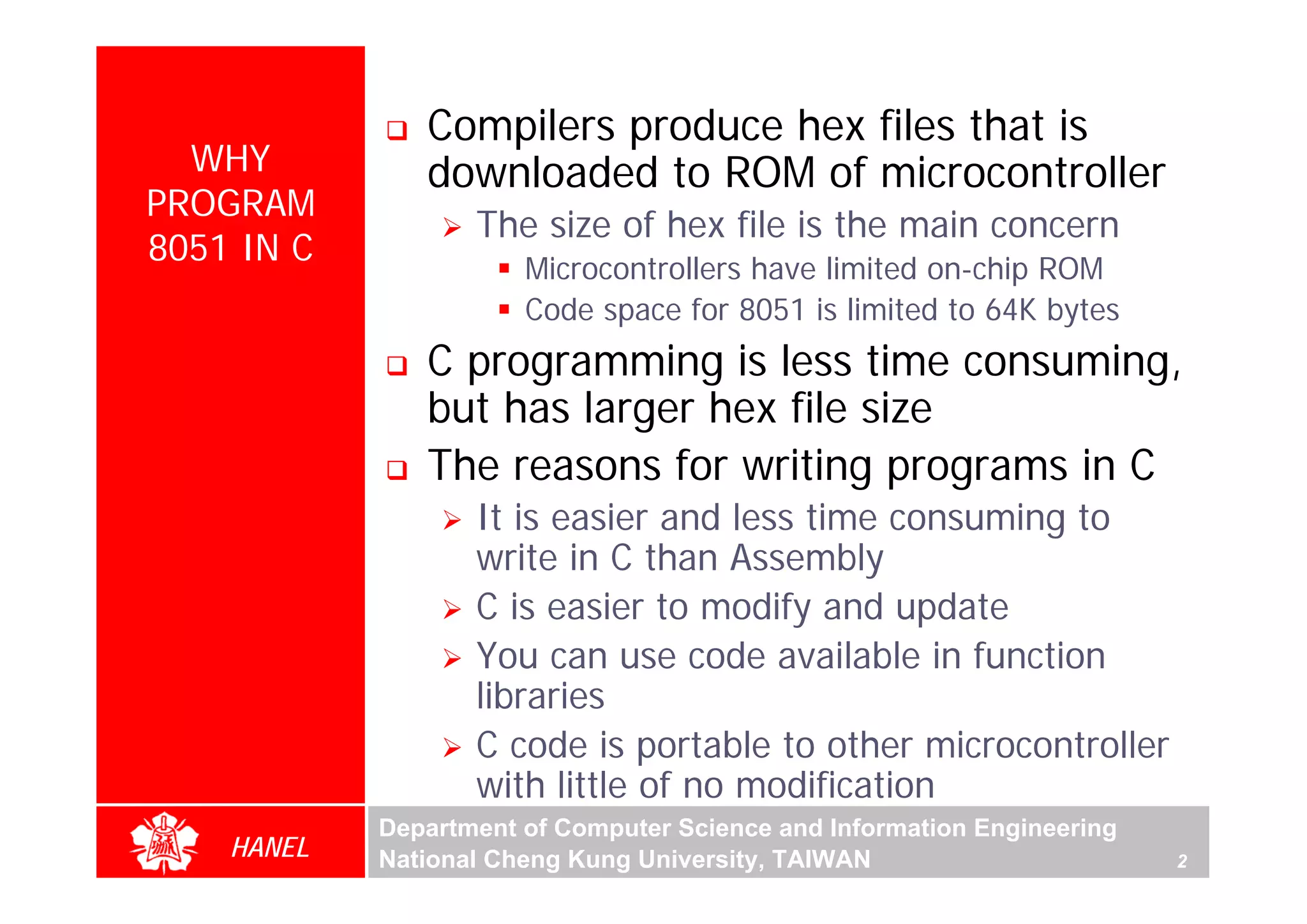
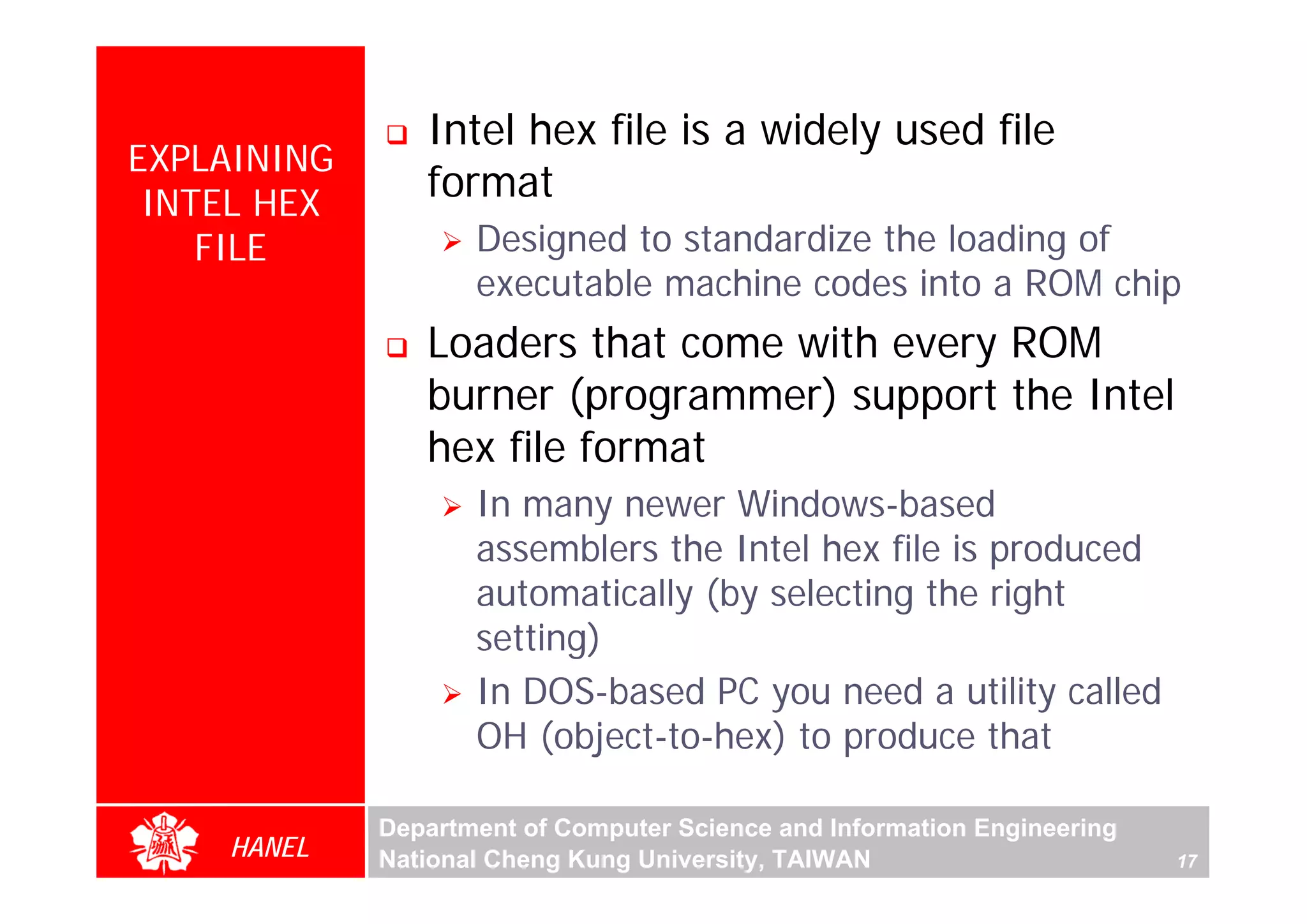
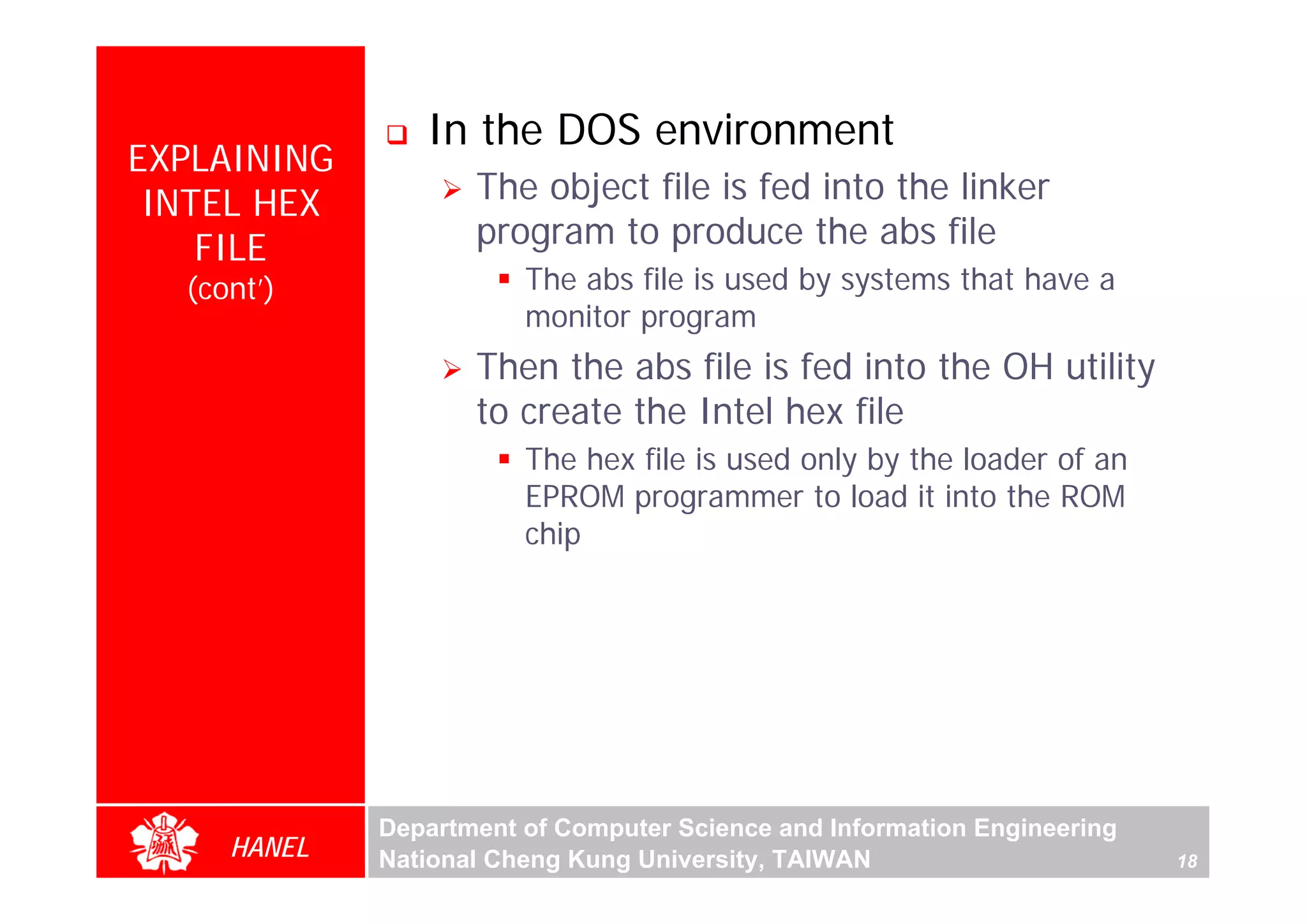
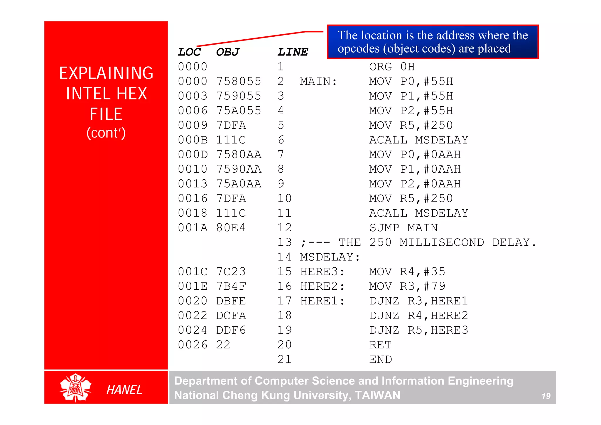
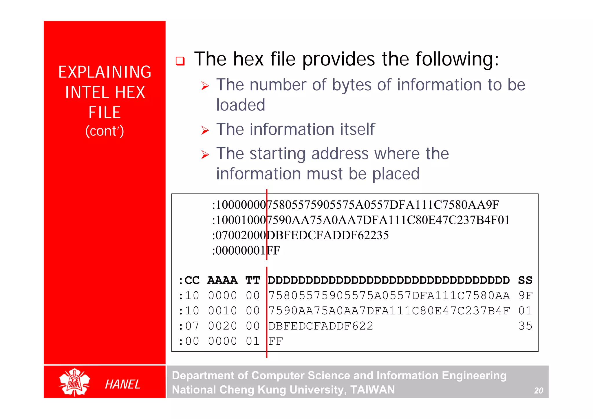
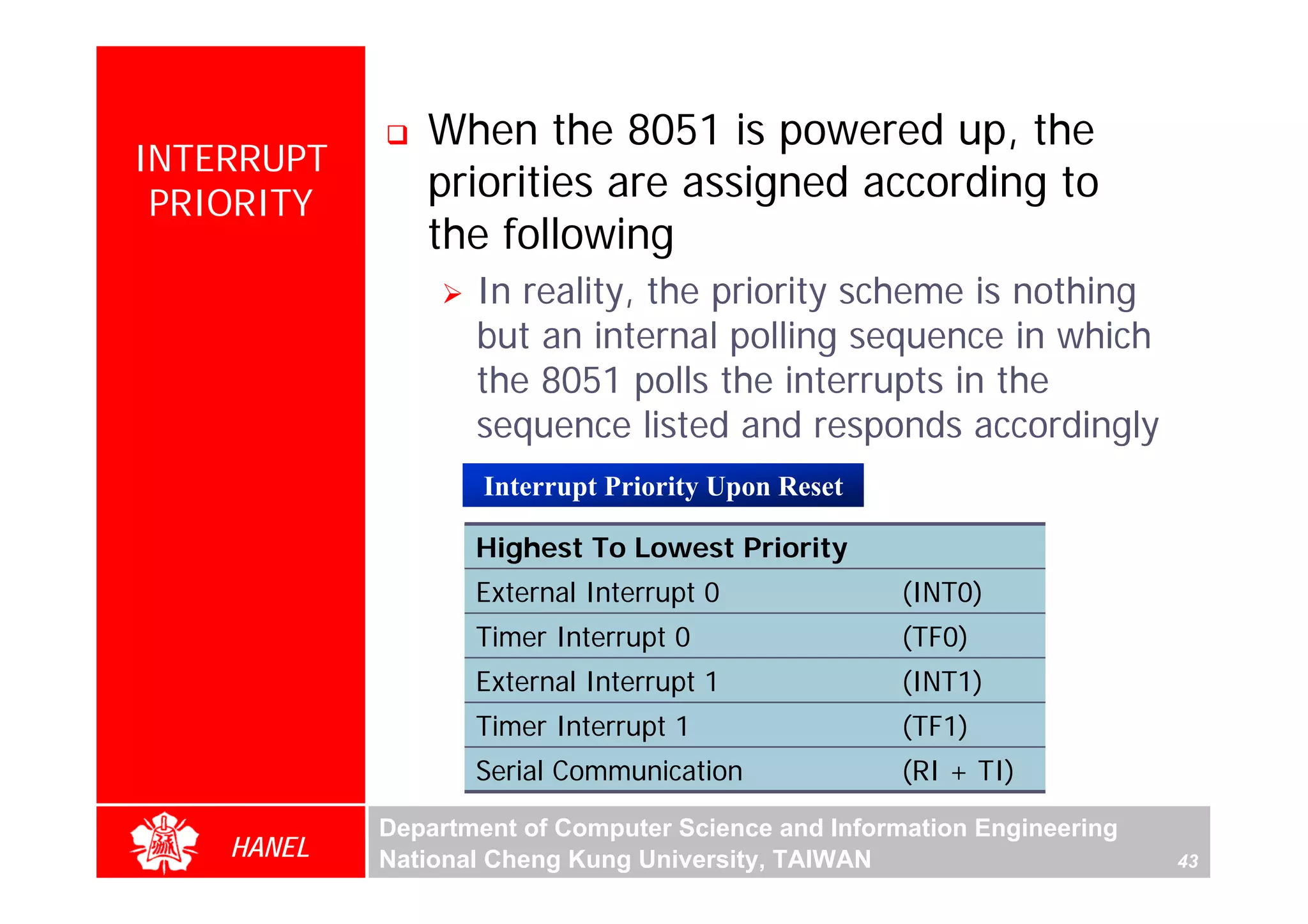
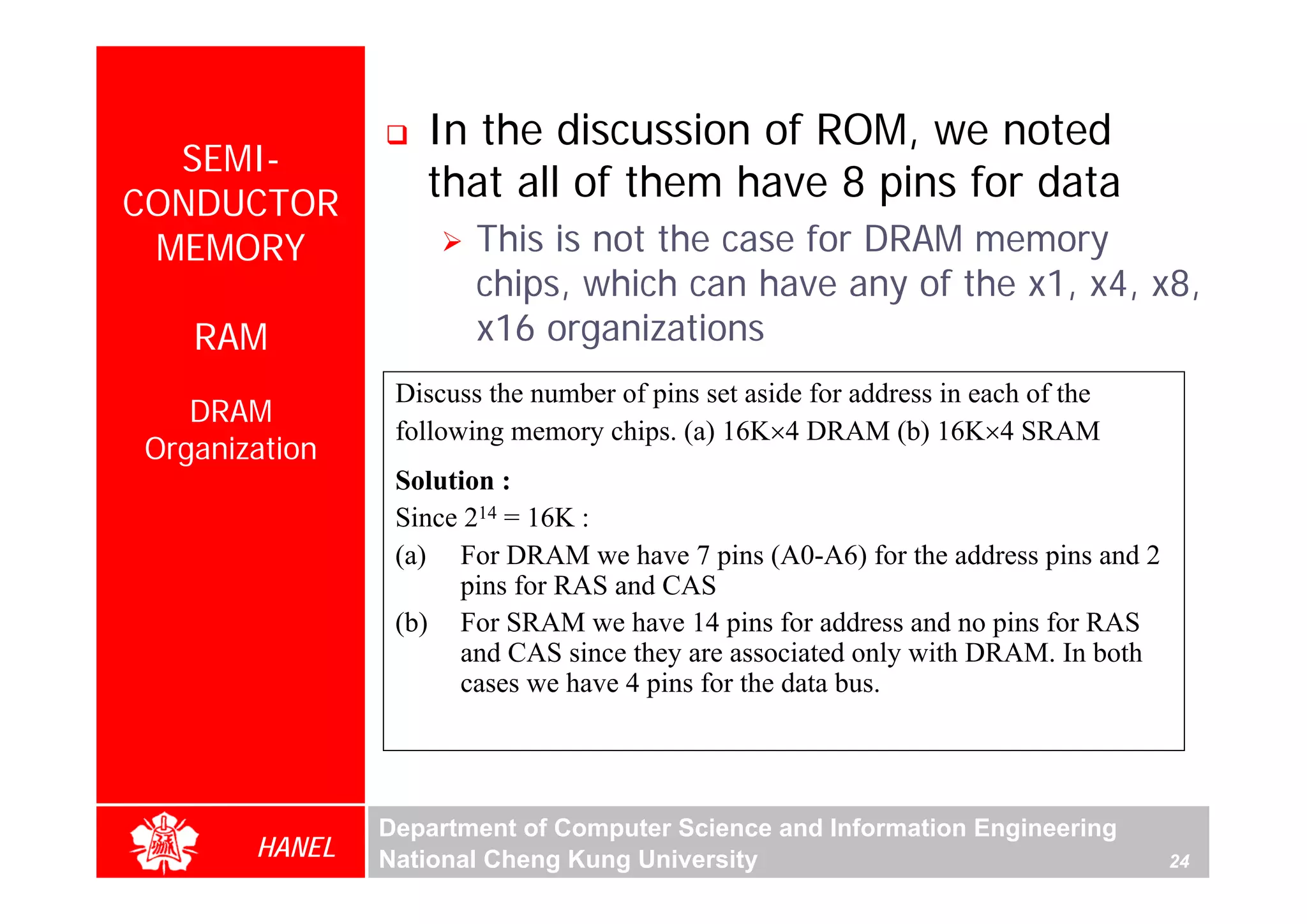
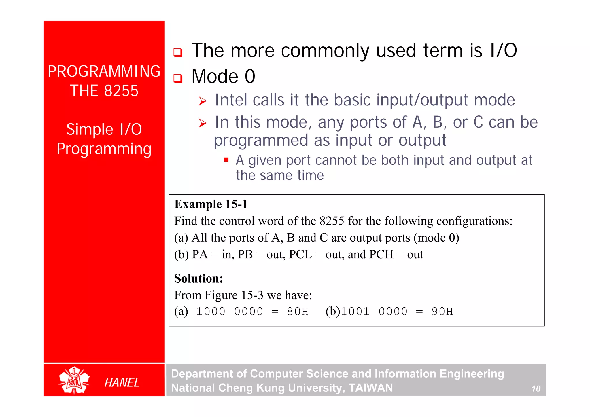
Downloaded 333 times

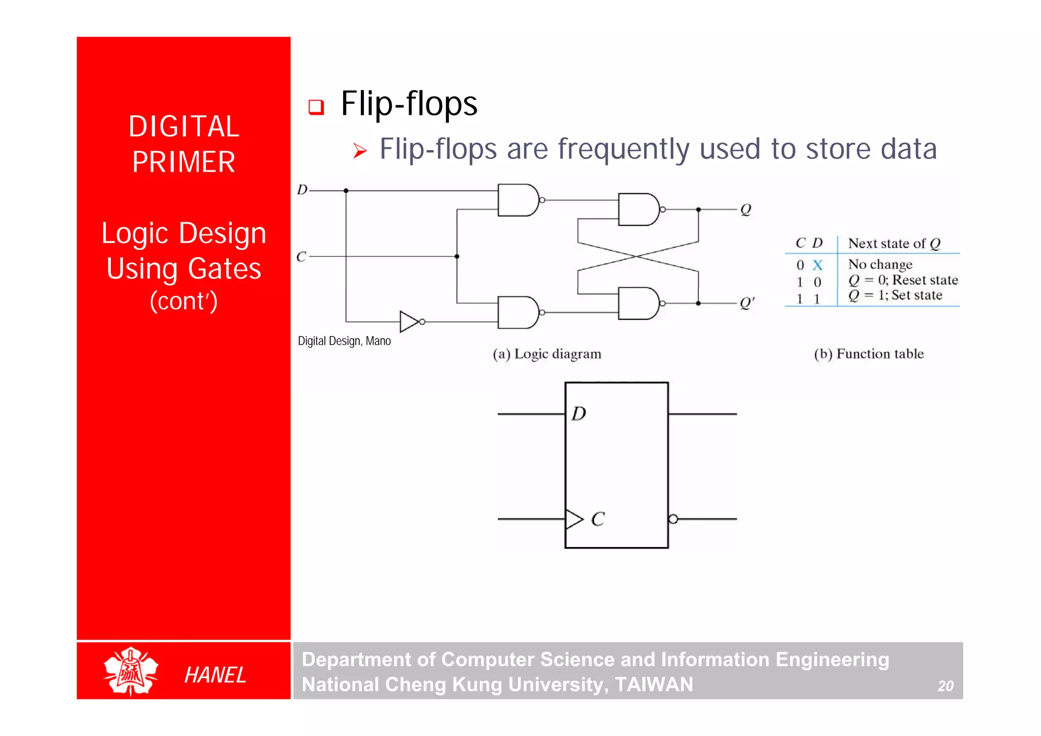

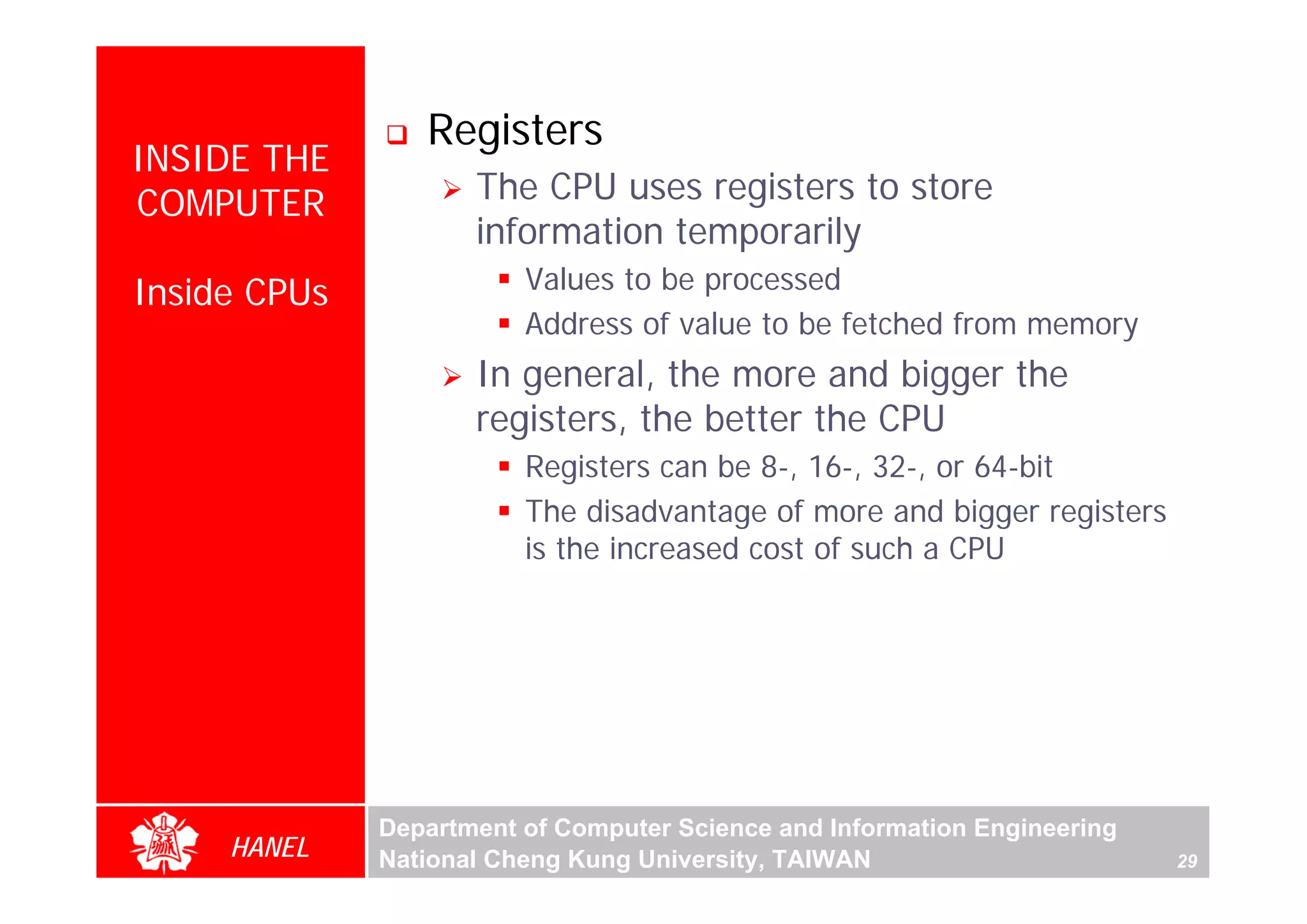
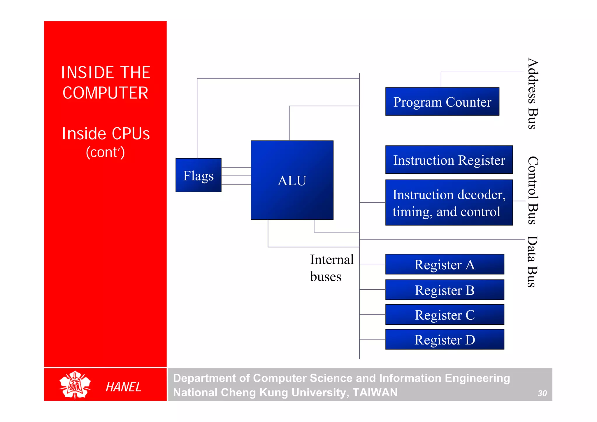
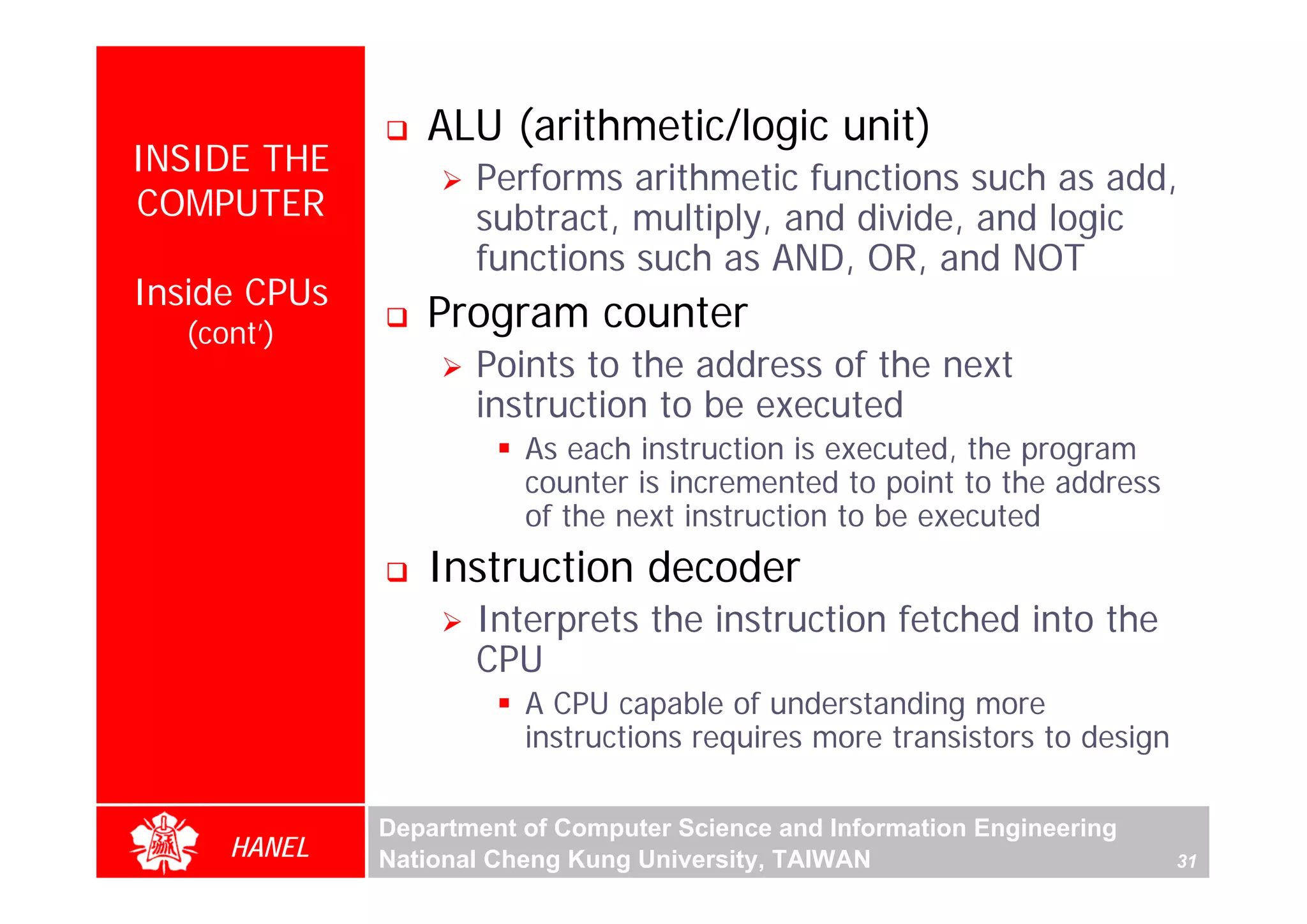
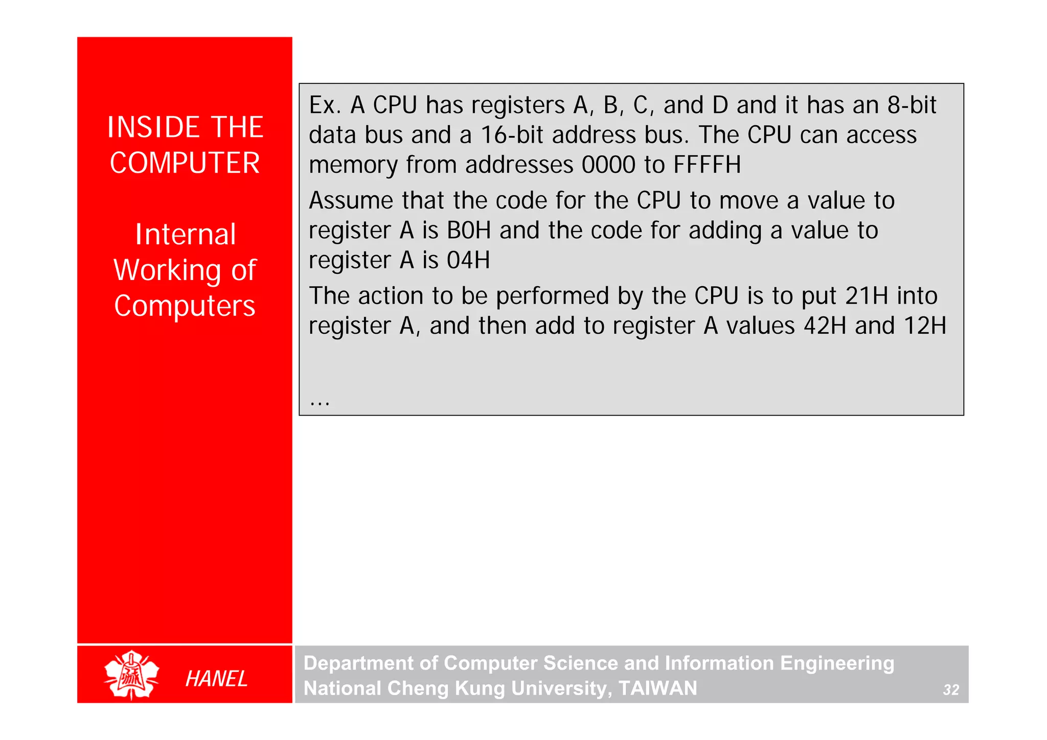
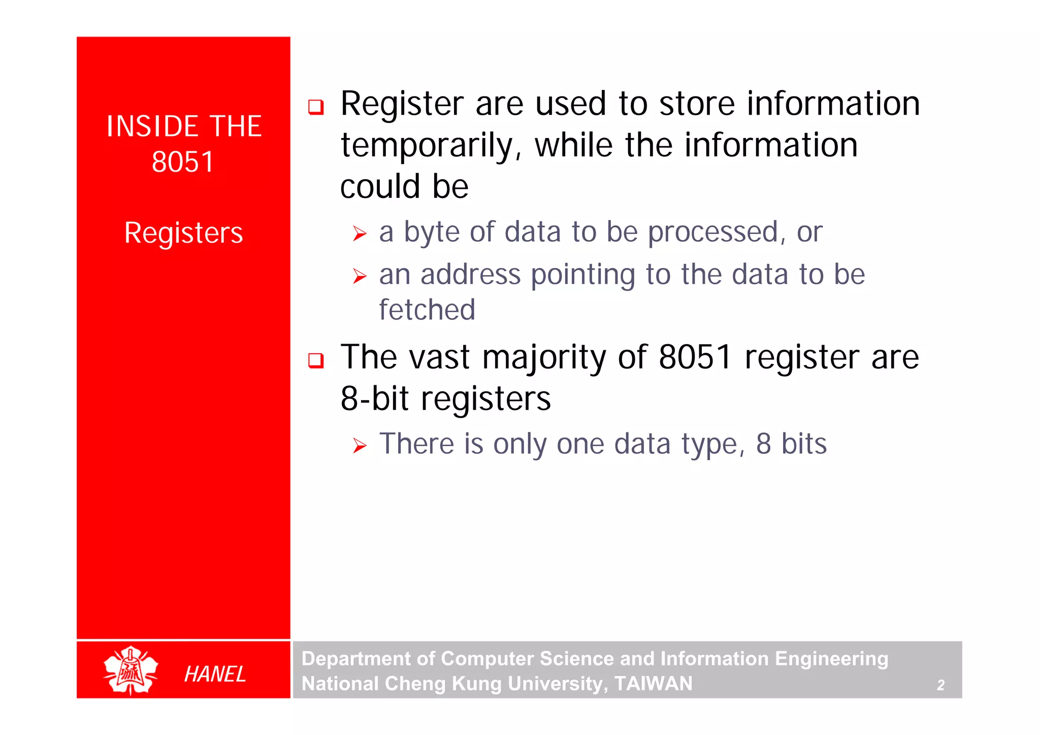
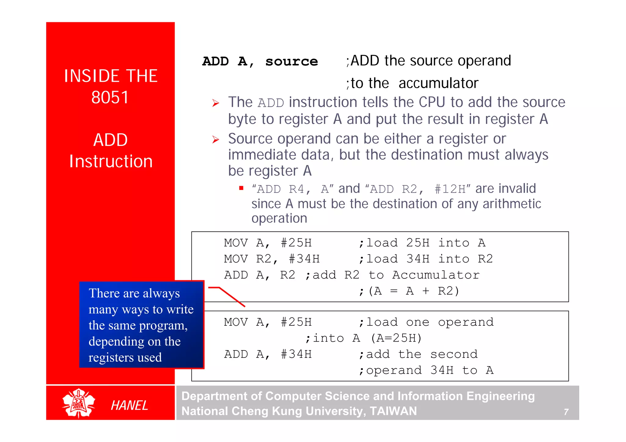
![An Assembly language instruction
8051
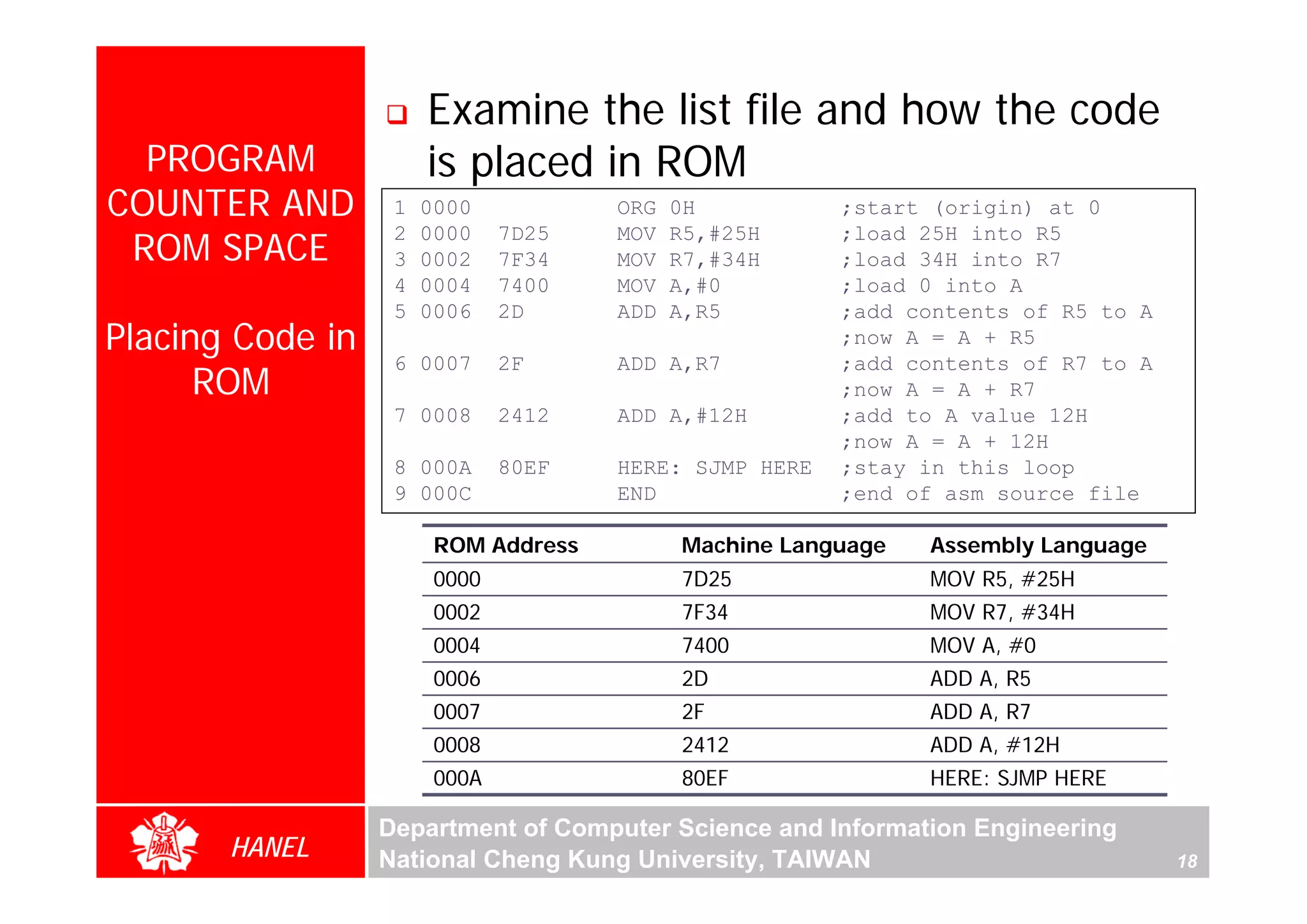
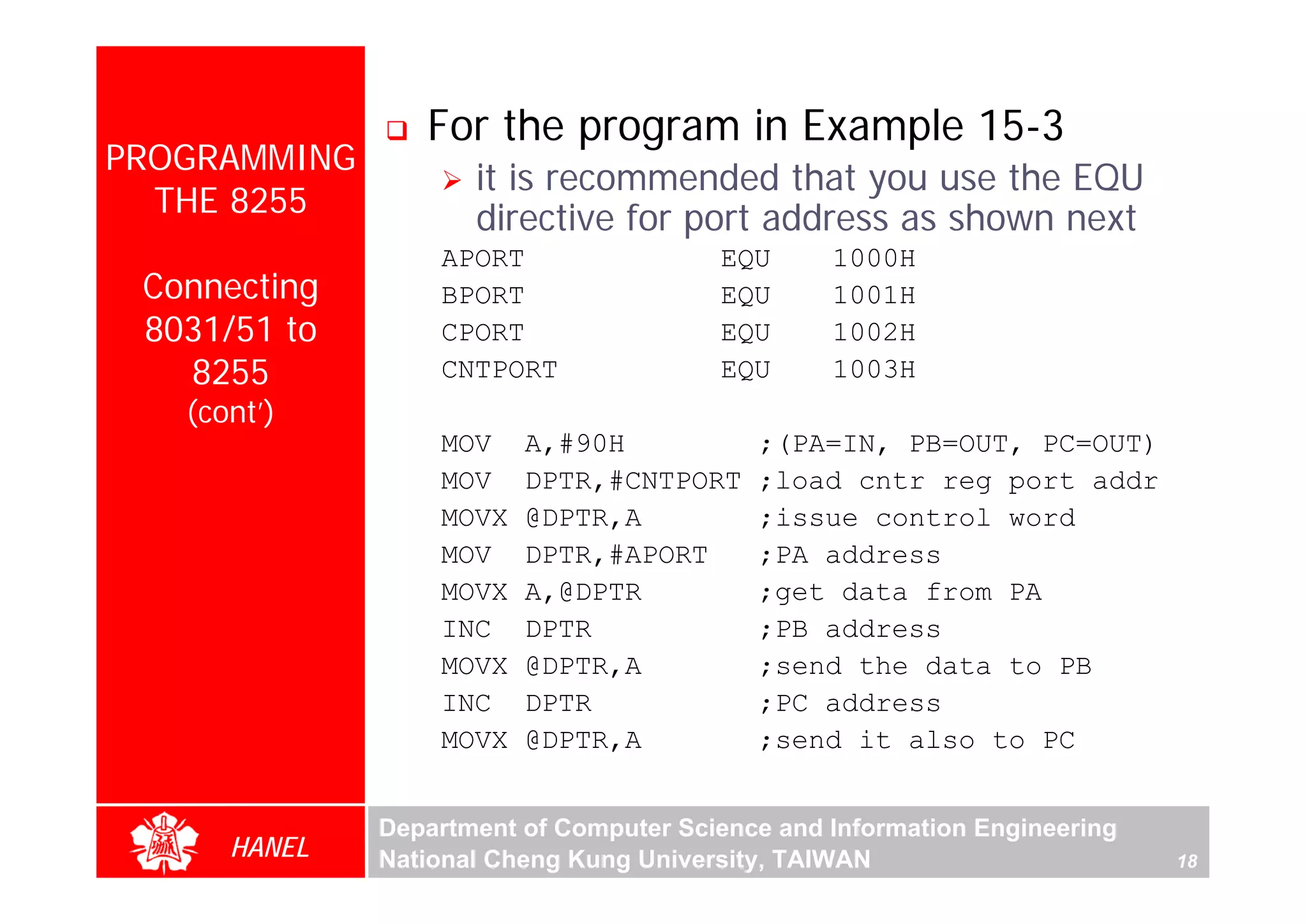
ASSEMBLY consists of four fields:
PROGRAMMING [label:] Mnemonic [operands] [;comment]
ORG 0H ;start(origin) at location
Structure of 0
MOV R5, #25H ;load 25H into R5
Assembly MOV R7, #34H ;load 34H into R7 Directives do not
Language MOV A, #0 ;load 0 into generate any machine
A
ADD A, R5 ;add contents ofand are used
code R5 to A
;now A = A + only by the assembler
R5
Mnemonics ADD A, R7 ;add contents of R7 to A
produce ;now A = A + R7
opcodes ADD A, #12H ;add to A value 12H
;now A = A + 12H
HERE: SJMP HERE ;stay in this loop
END ;end of asm may be at the end of a
Comments source file
The label field allows line or on a line by themselves
the program to refer to a The assembler ignores comments
line of code by name
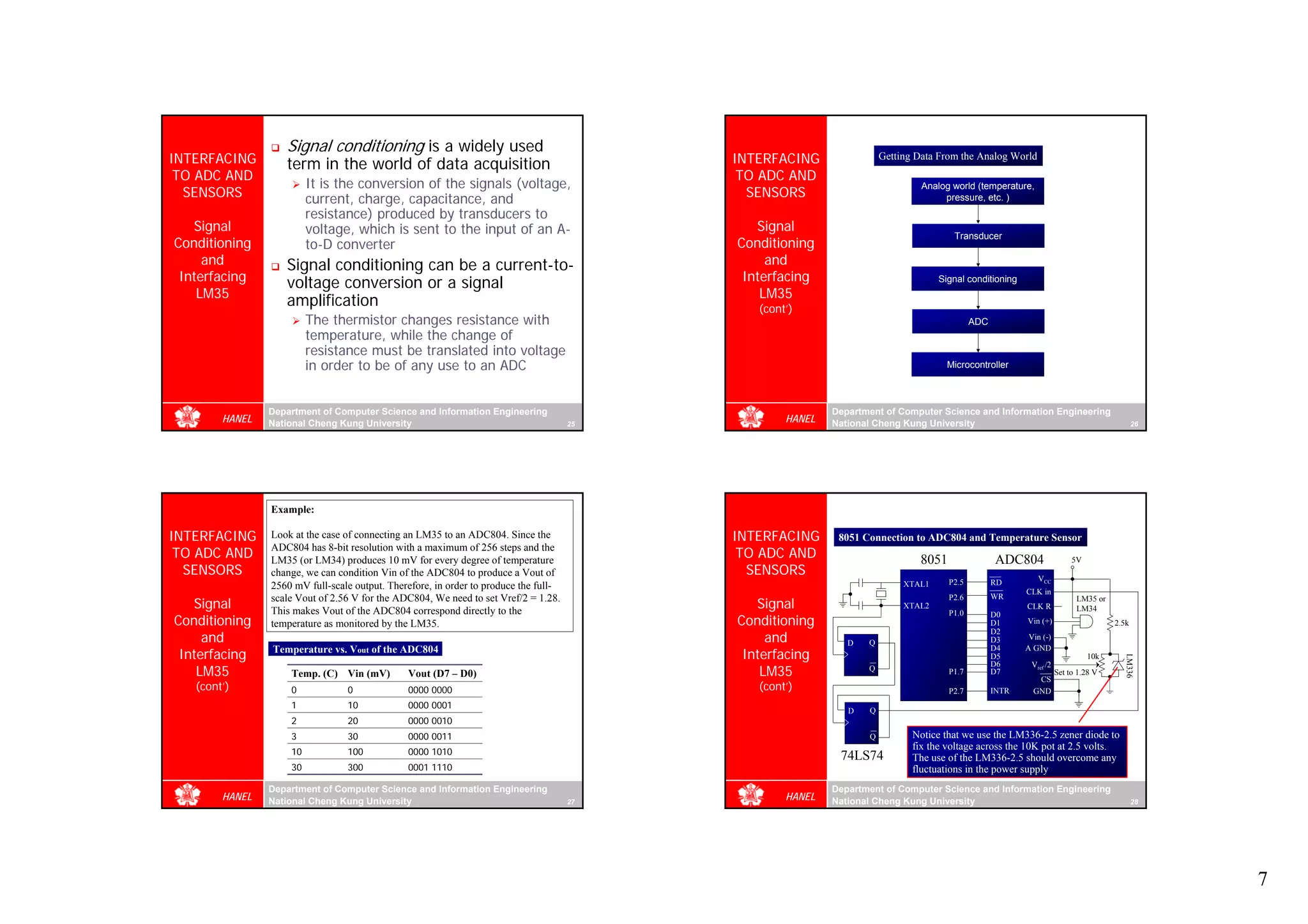
Department of Computer Science and Information Engineering
HANEL National Cheng Kung University, TAIWAN 10](https://image.slidesharecdn.com/the8051microcontrollerandembeddedsystemsusingassemblyandc-2nd-ed-120504220416-phpapp02/75/The-8051-microcontroller-and-embedded-systems-using-assembly-and-c-2nd-ed-66-2048.jpg)
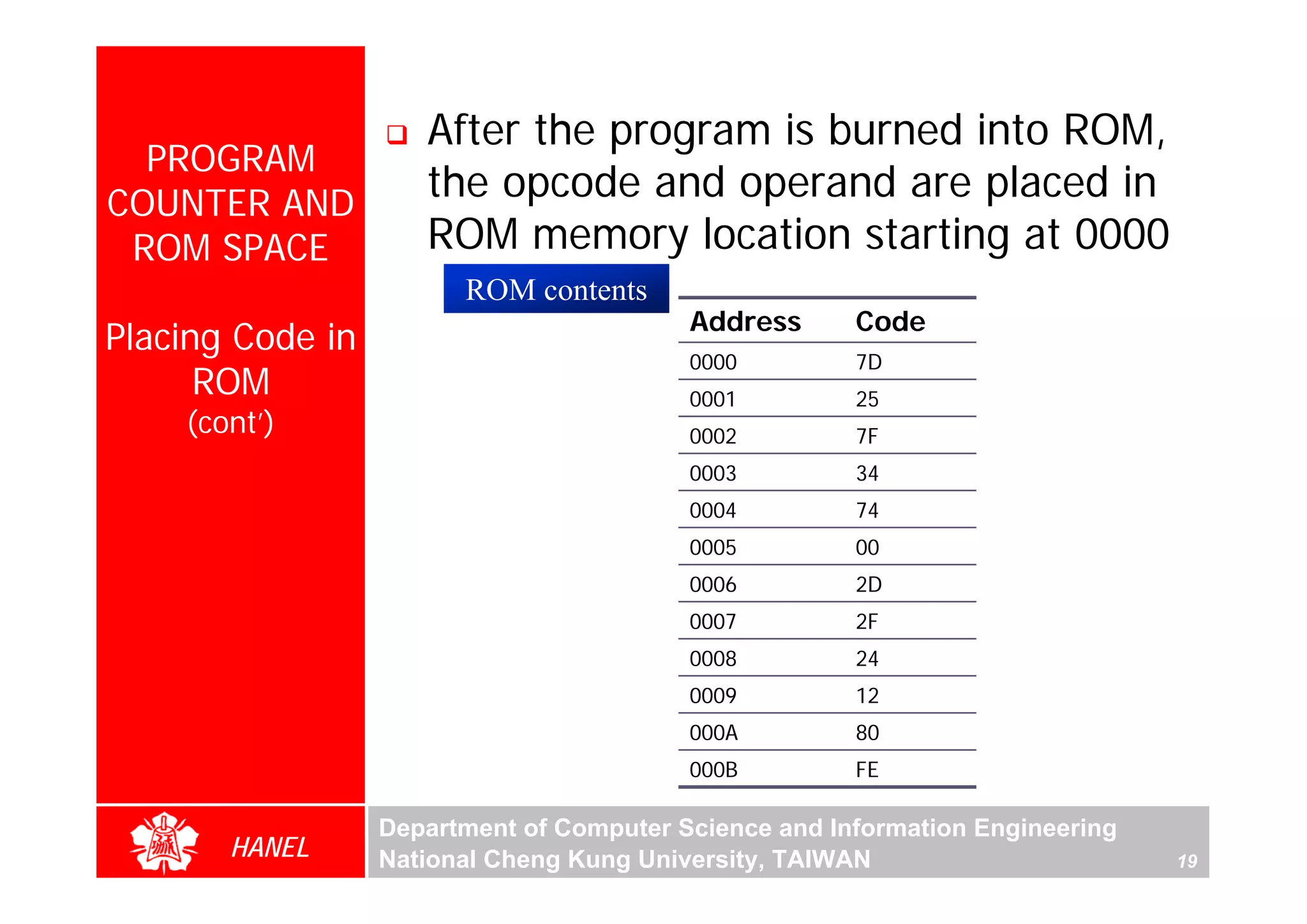

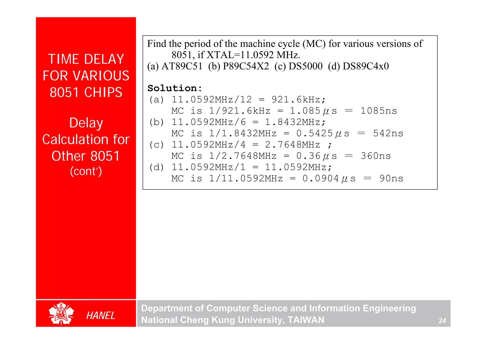
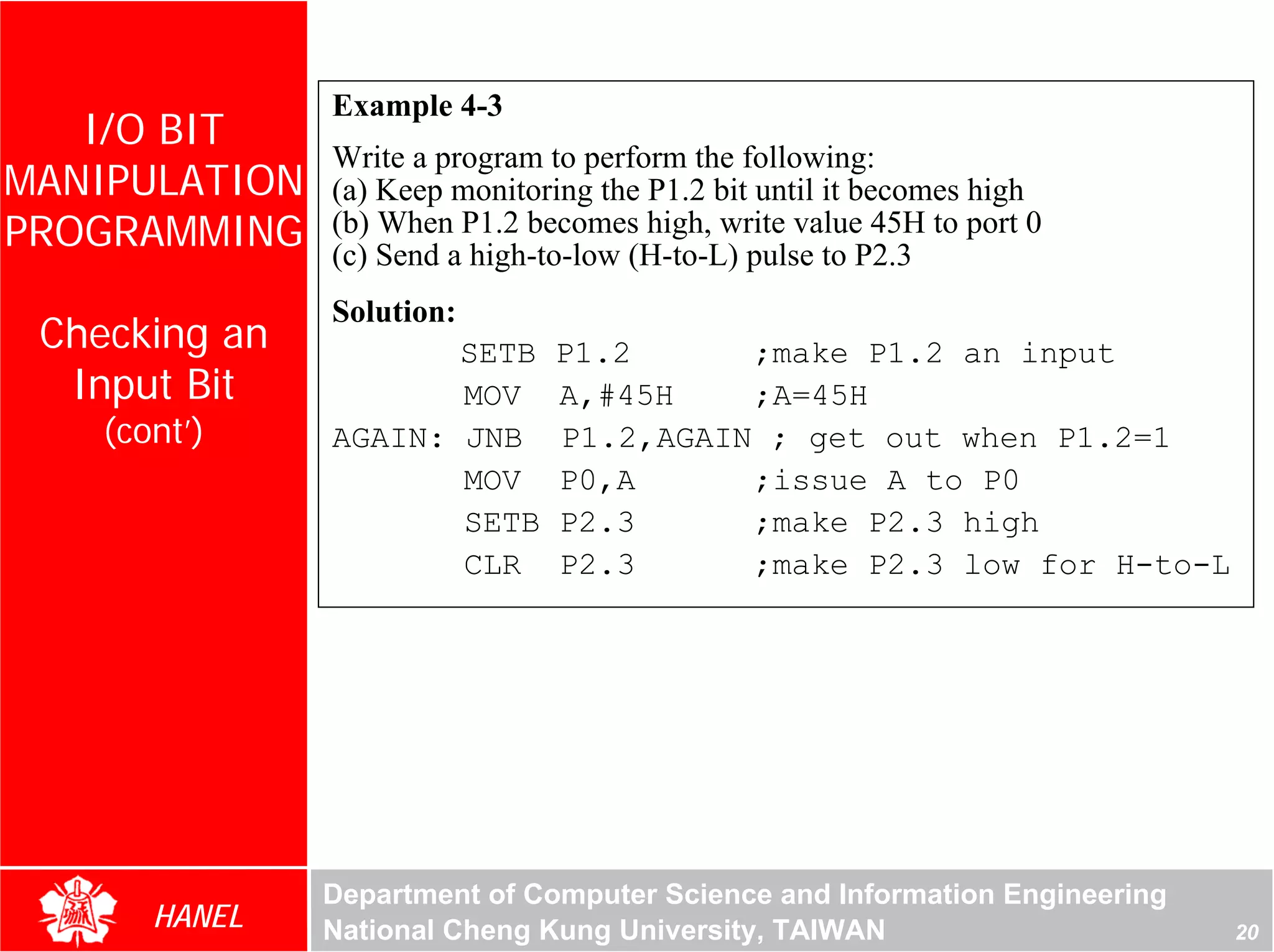
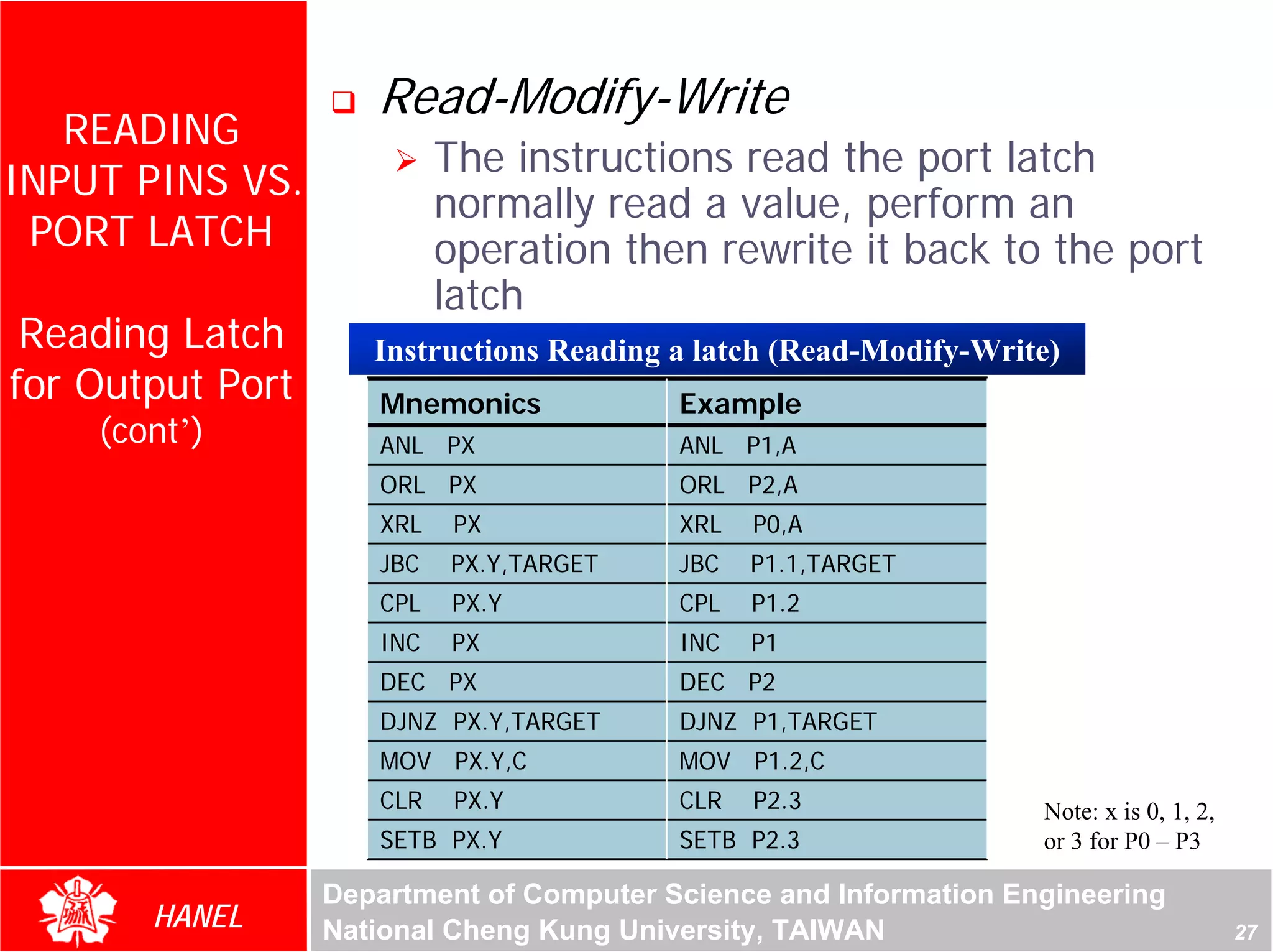
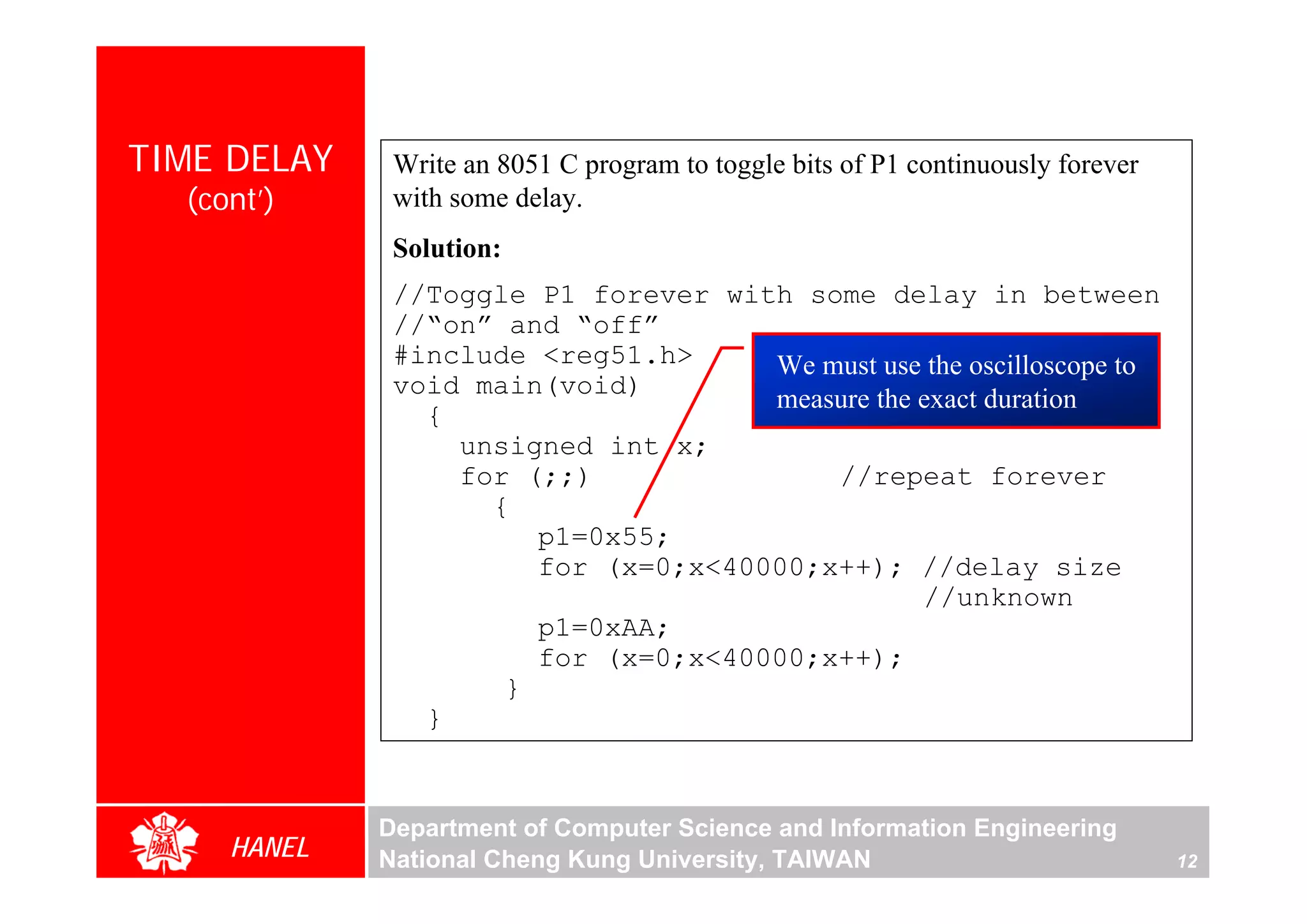
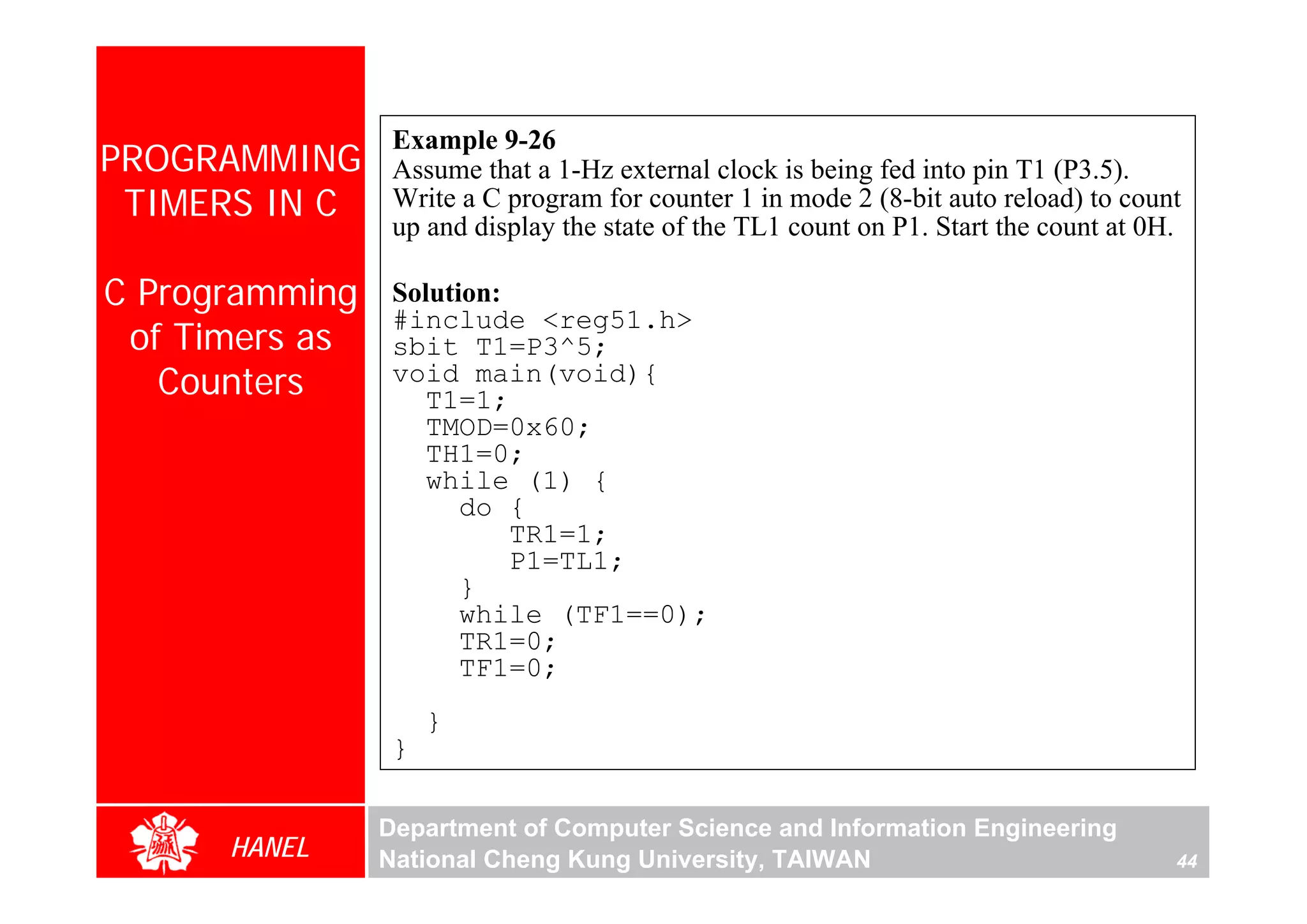
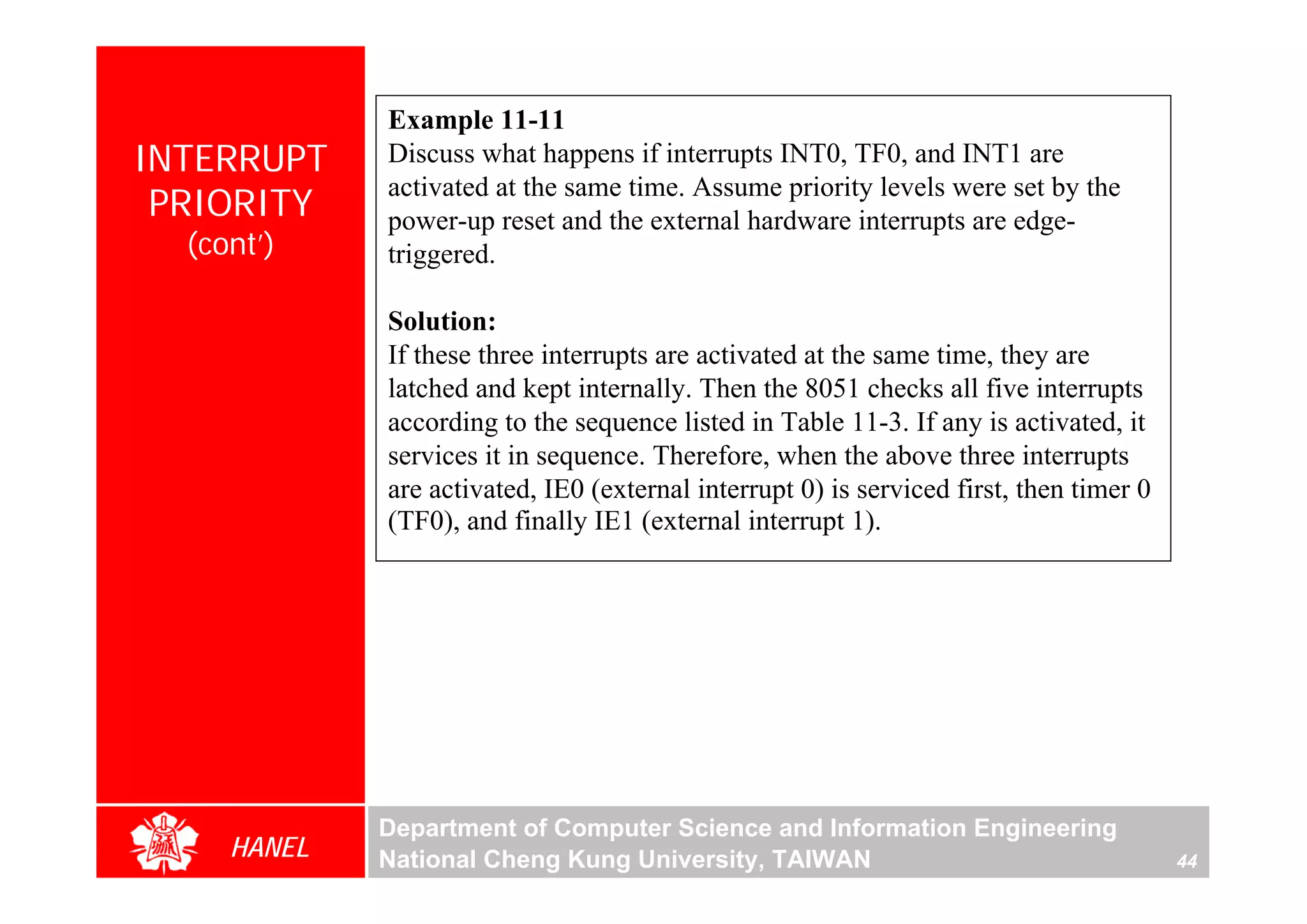
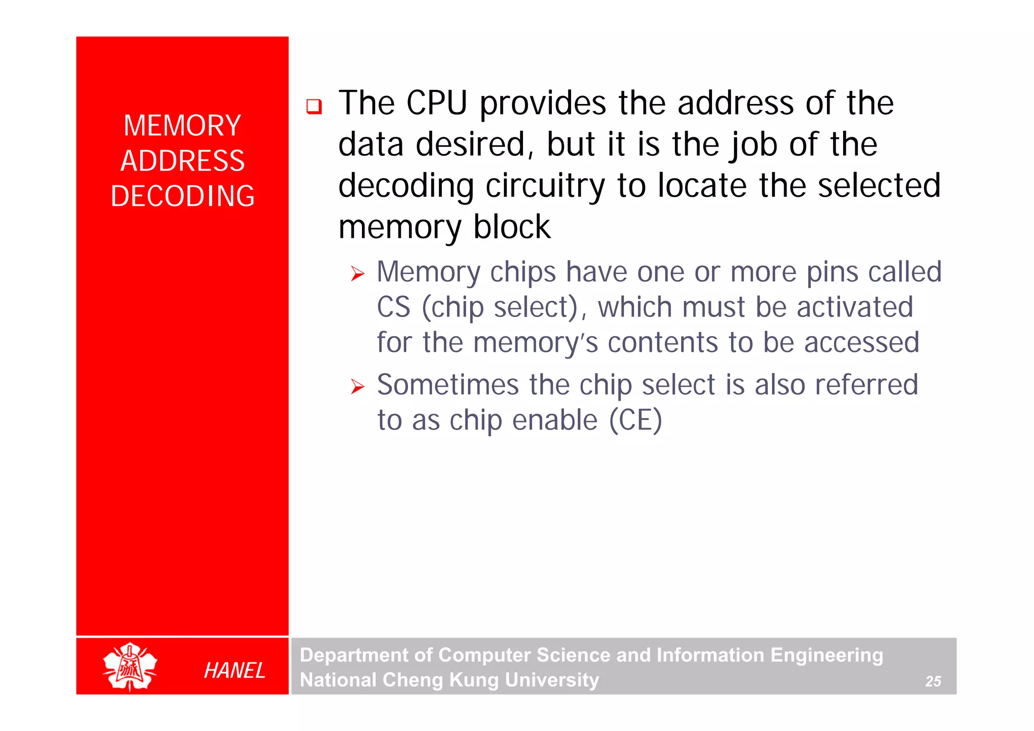
![Find the size of the delay in following program, if the crystal
TIME DELAY frequency is 11.0592MHz.
FOR VARIOUS
8051 CHIPS MOV A,#55H
AGAIN: MOV P1,A
ACALL DELAY
Delay CPL A
Calculation SJMP AGAIN A simple way to short jump
to itself in order to keep the
;---time delay-------
DELAY: MOV R3,#200 microcontroller busy
HERE: DJNZ R3,HERE HERE: SJMP HERE
RET We can use the following:
SJMP $
Solution:
Machine cycle
DELAY: MOV R3,#200 1
HERE: DJNZ R3,HERE 2
RET 2
Therefore, [(200x2)+1+2]x1.085μs = 436.255μs.
Department of Computer Science and Information Engineering
HANEL National Cheng Kung University, TAIWAN 20](https://image.slidesharecdn.com/the8051microcontrollerandembeddedsystemsusingassemblyandc-2nd-ed-120504220416-phpapp02/75/The-8051-microcontroller-and-embedded-systems-using-assembly-and-c-2nd-ed-123-2048.jpg)
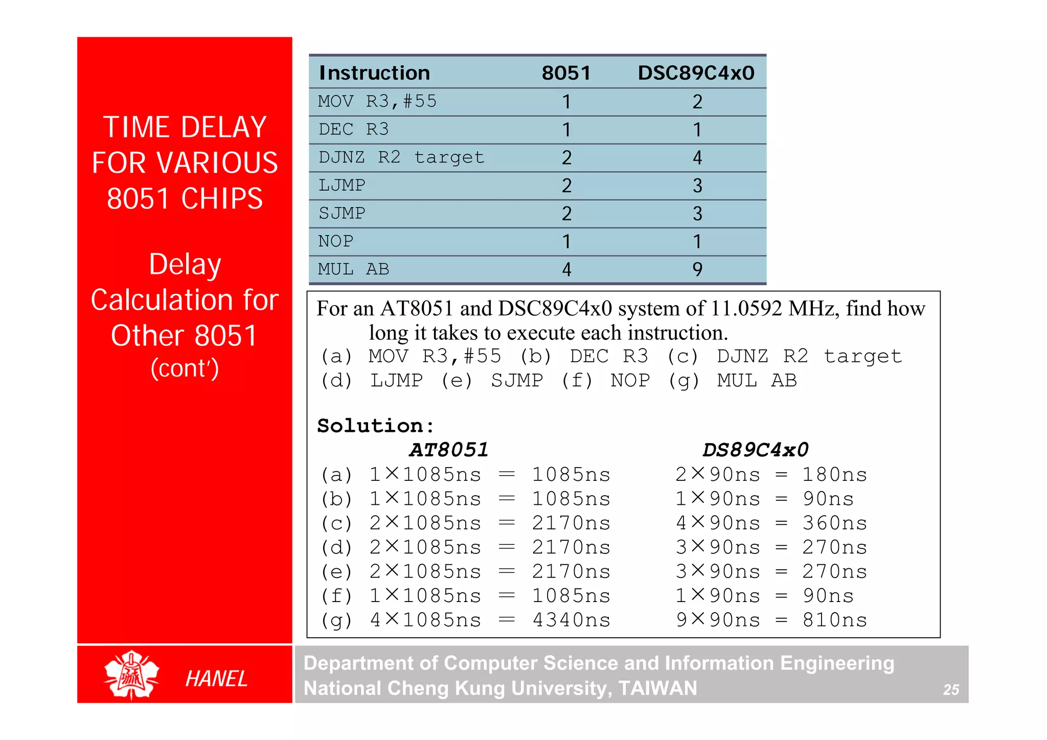
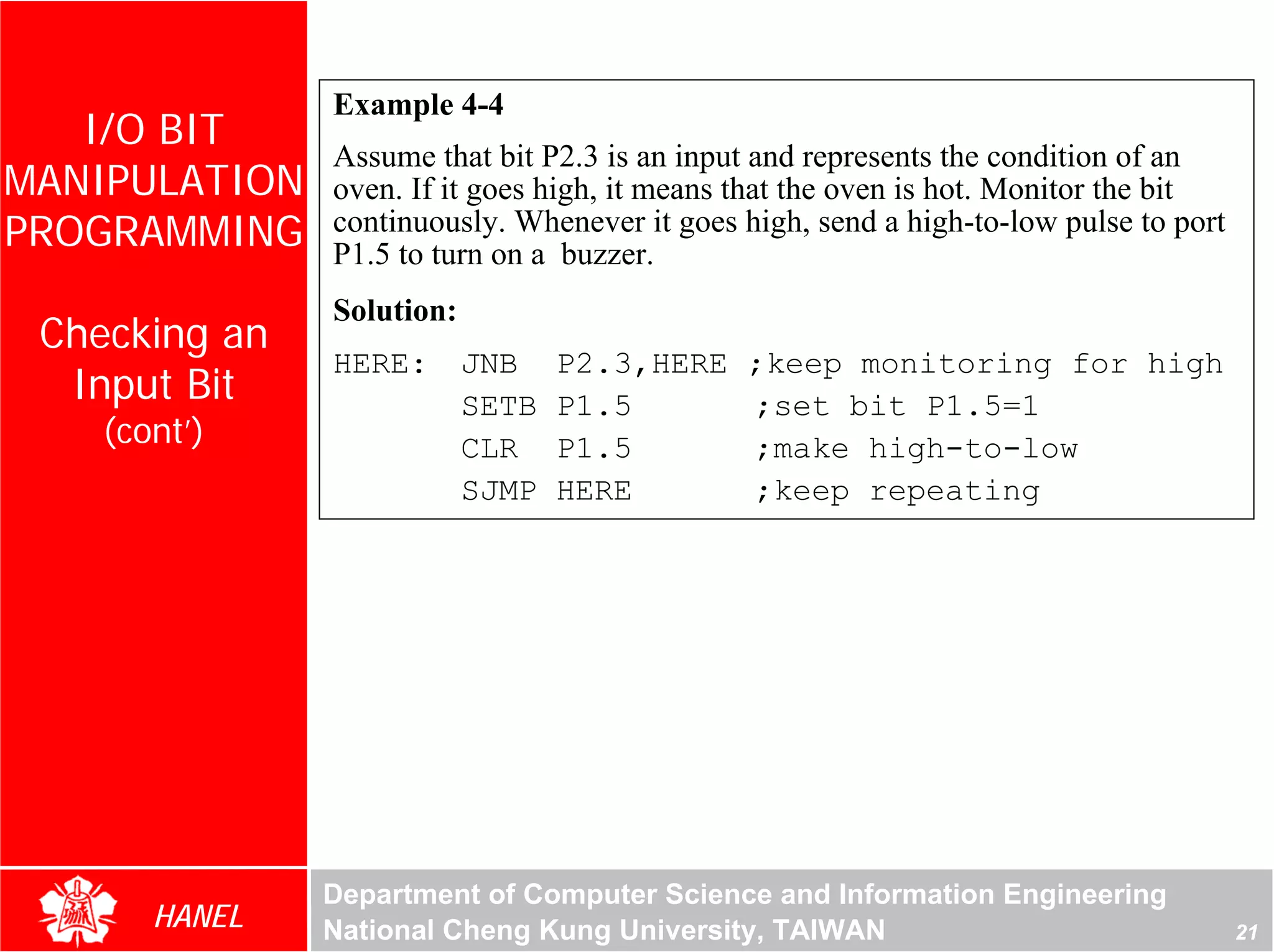
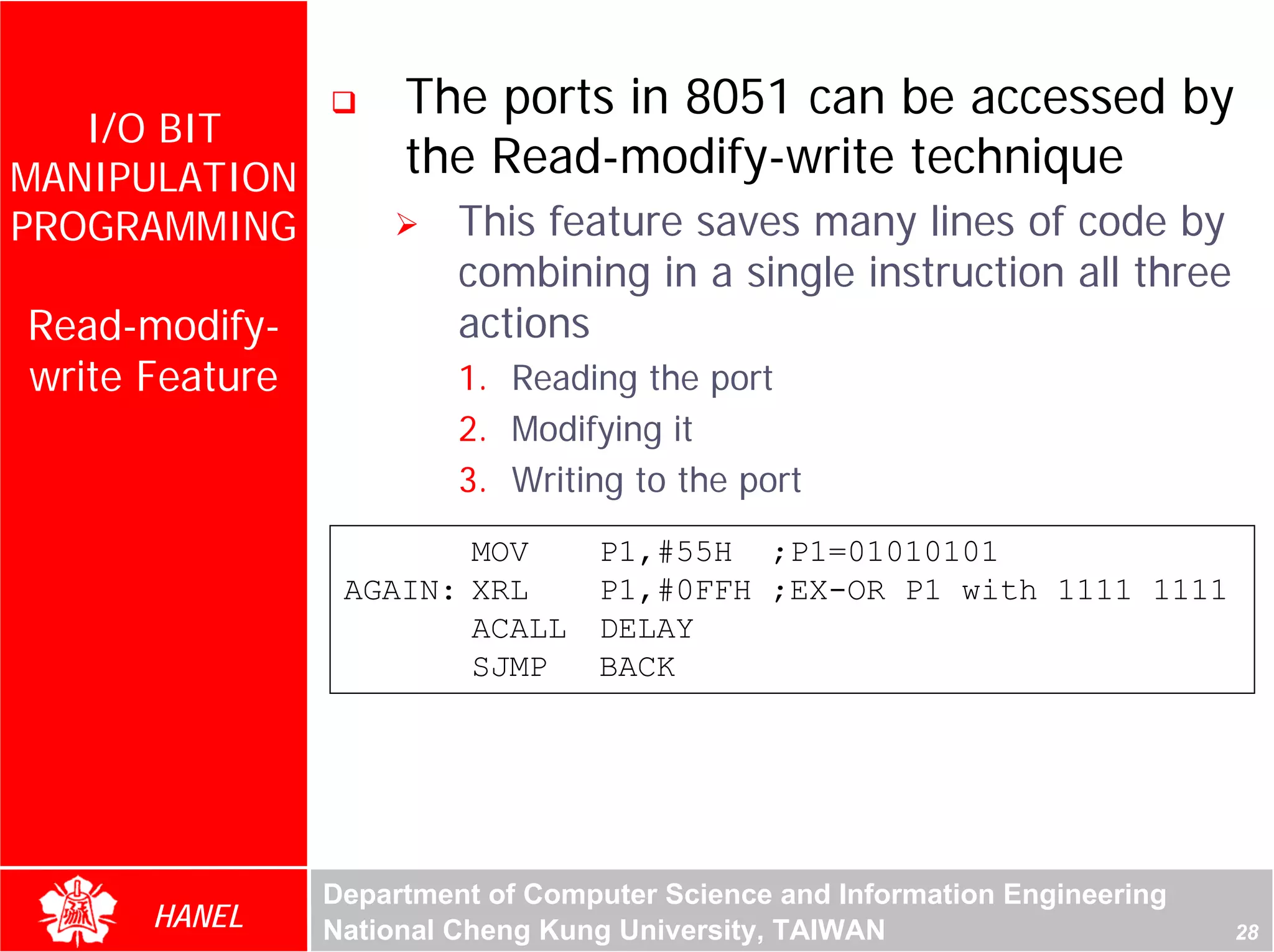
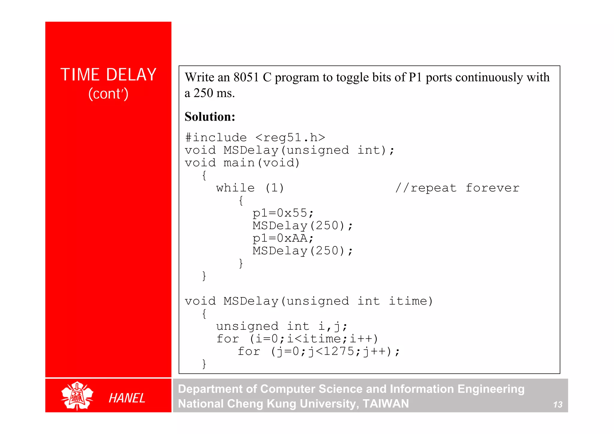
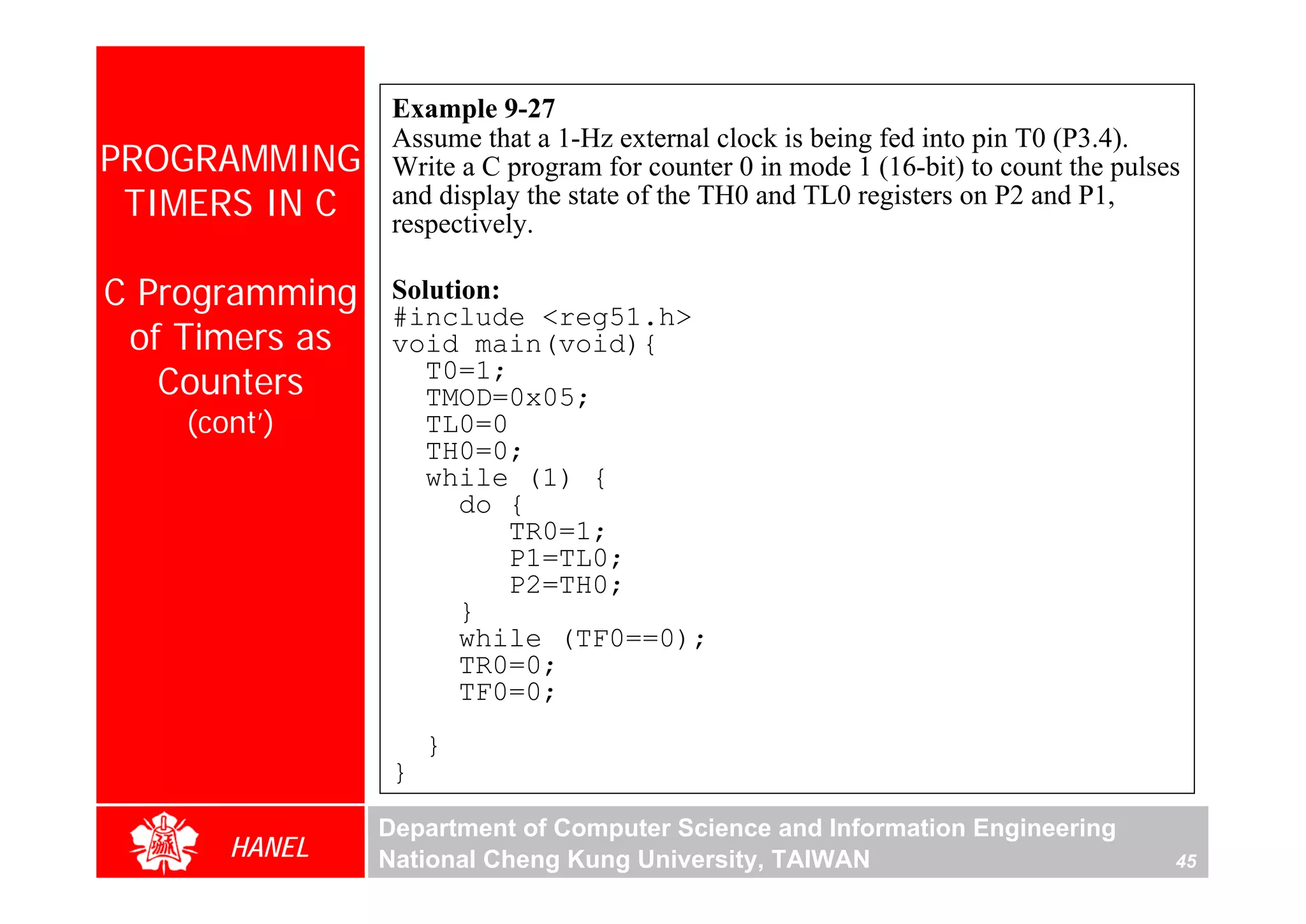
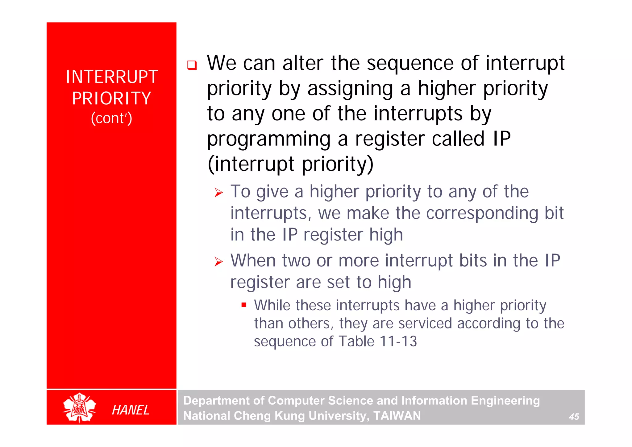
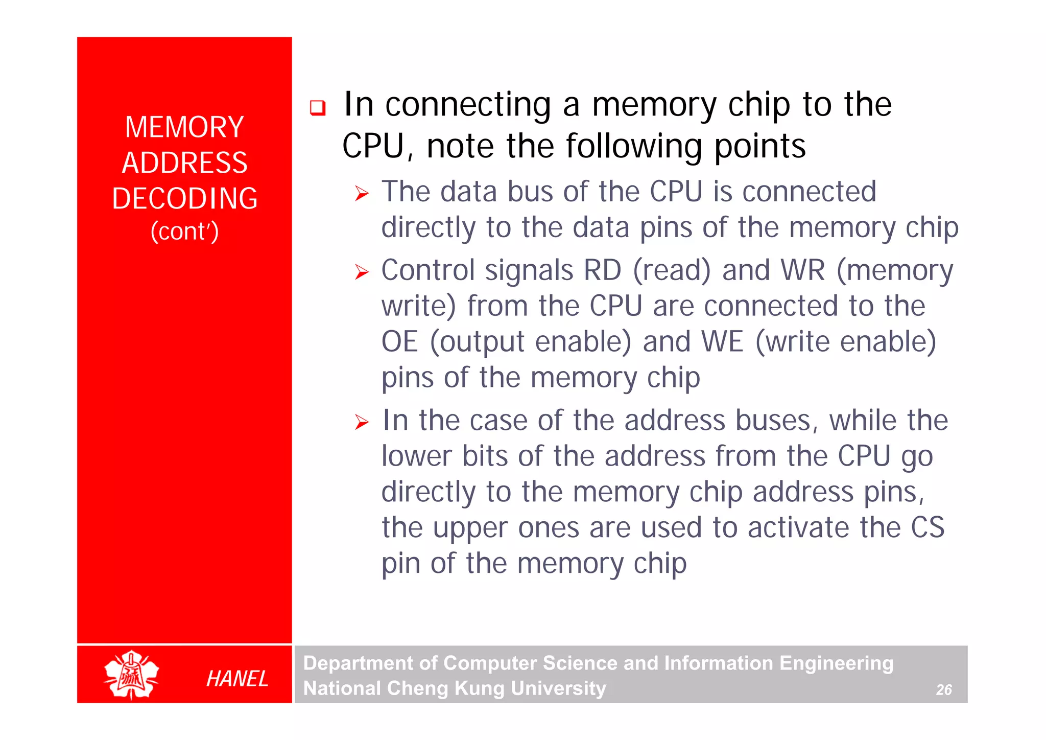
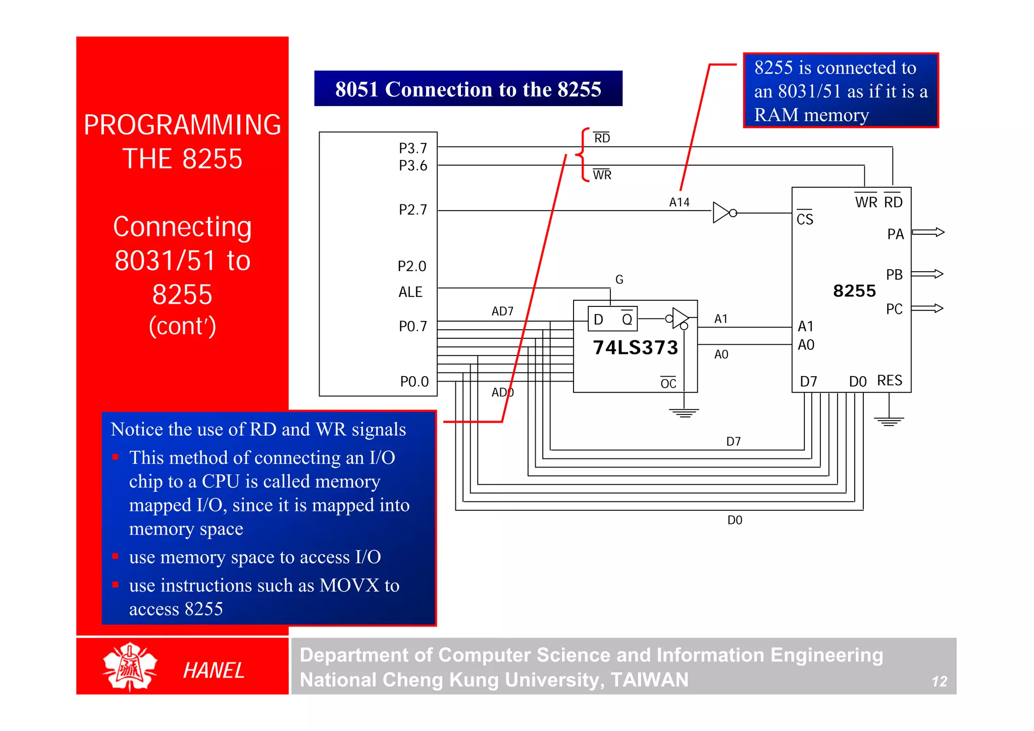
![Find the size of the delay in following program, if the crystal
TIME DELAY frequency is 11.0592MHz.
FOR VARIOUS
8051 CHIPS Machine Cycle
DELAY: MOV R3,#250 1
HERE: NOP 1
Increasing NOP 1
Delay Using NOP 1
NOP 1
NOP DJNZ R3,HERE 2
RET 2
Solution:
The time delay inside HERE loop is
[250(1+1+1+1+2)]x1.085μs = 1627.5μs.
Adding the two instructions outside loop we
have 1627.5μs + 3 x 1.085μs = 1630.755μs
Department of Computer Science and Information Engineering
HANEL National Cheng Kung University, TAIWAN 21](https://image.slidesharecdn.com/the8051microcontrollerandembeddedsystemsusingassemblyandc-2nd-ed-120504220416-phpapp02/75/The-8051-microcontroller-and-embedded-systems-using-assembly-and-c-2nd-ed-124-2048.jpg)


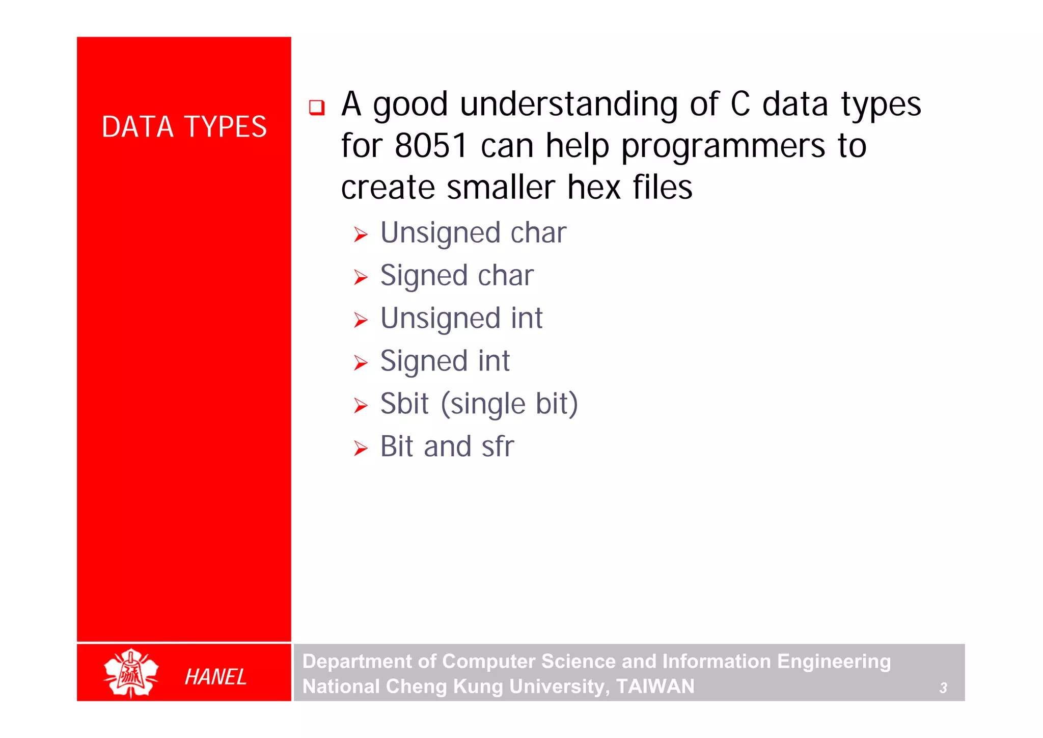
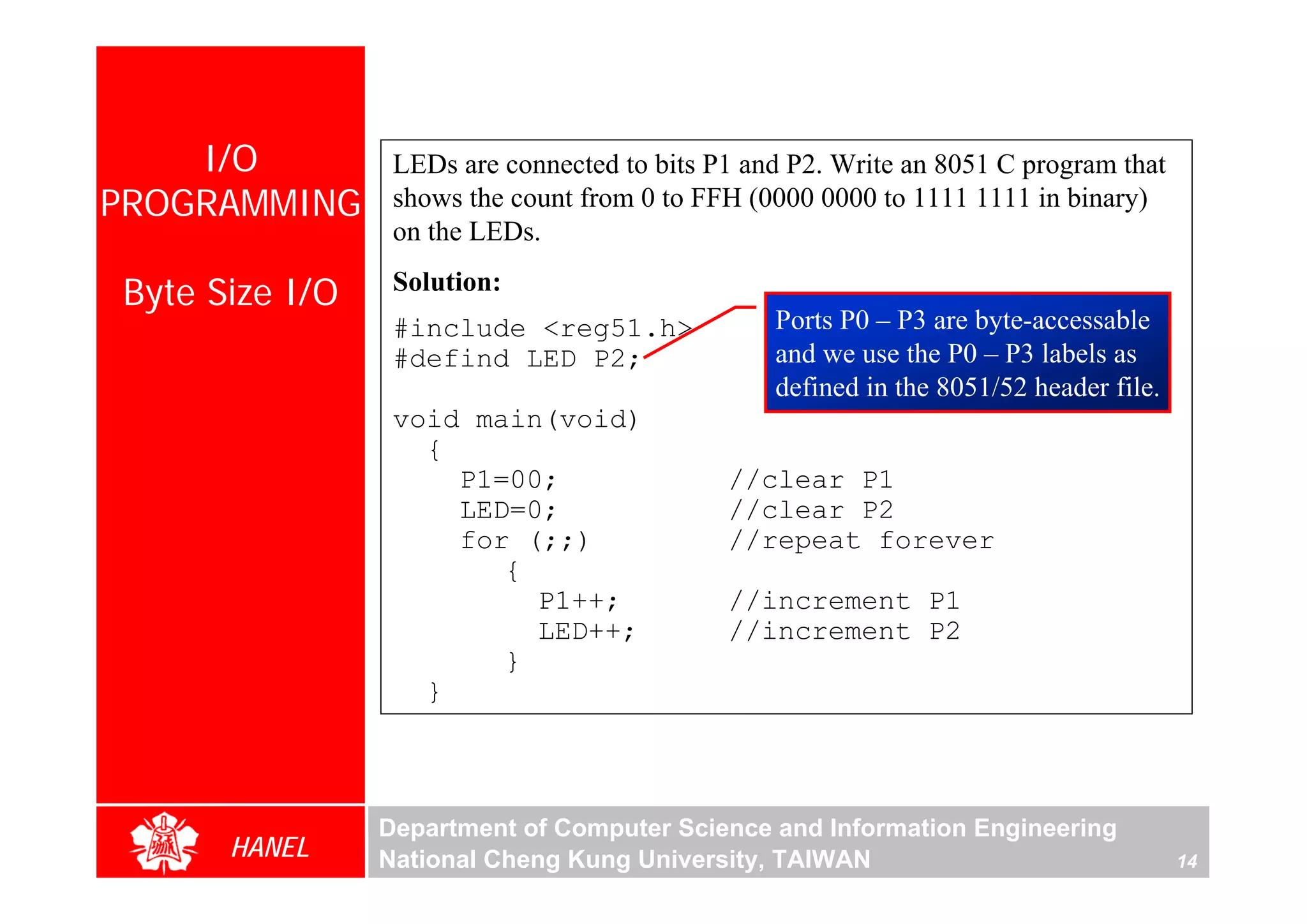
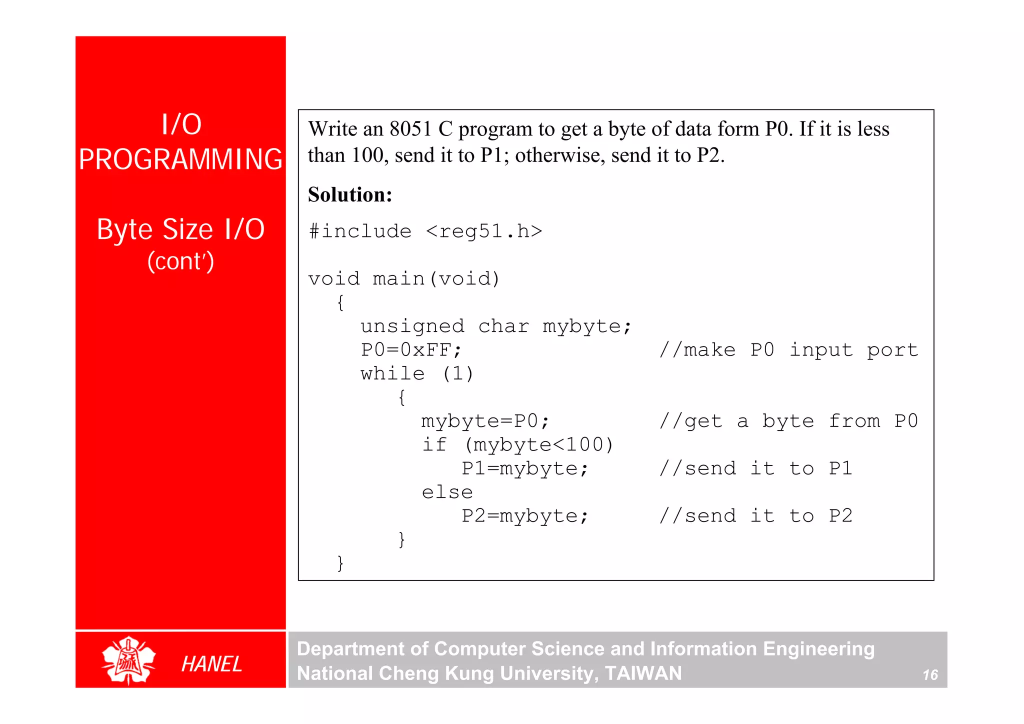
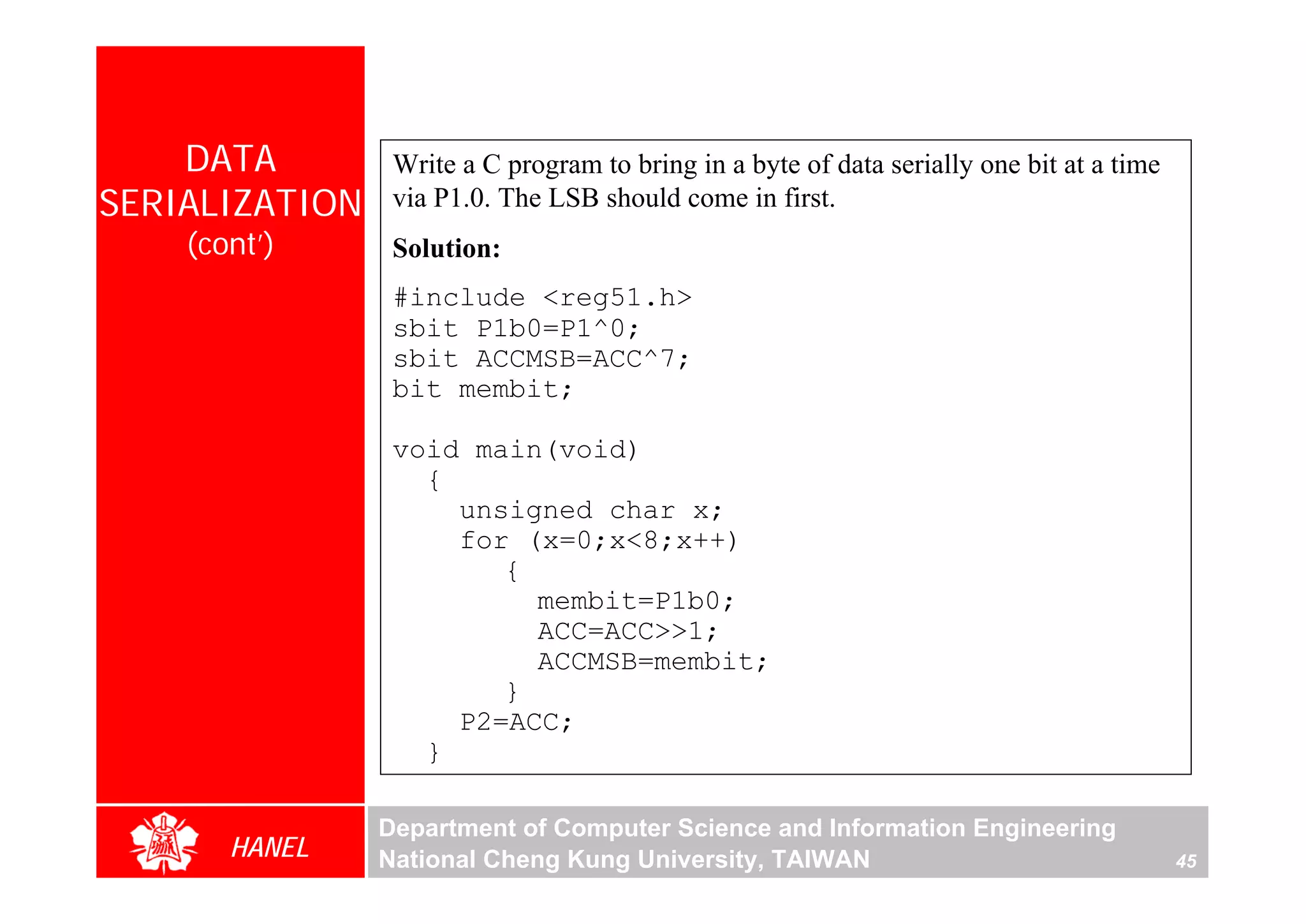
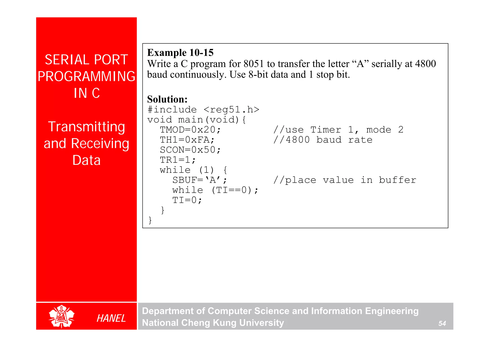
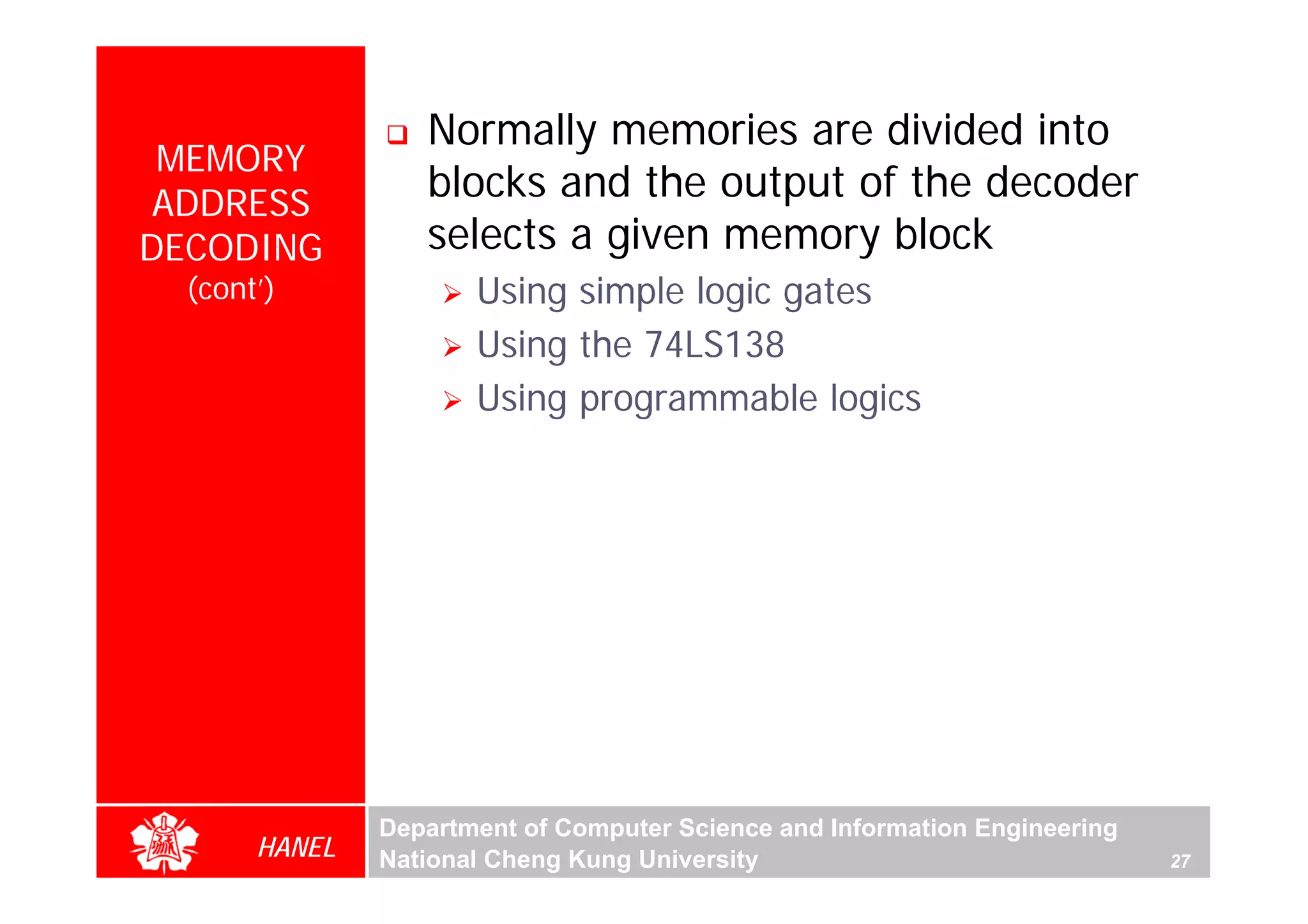
![Write an 8051 C program to send values 00 – FF to port P1.
Solution:
DATA TYPES 1. Pay careful attention to
#include <reg51.h> the size of the data
void main(void) 2. Try to use unsigned char
Unsigned char { instead of int if possible
(cont’) unsigned char z;
for (z=0;z<=255;z++)
P1=z;
}
Write an 8051 C program to send hex values for ASCII characters of
0, 1, 2, 3, 4, 5, A, B, C, and D to port P1.
Solution:
#include <reg51.h>
void main(void)
{
unsigned char mynum[]=“012345ABCD”;
unsigned char z;
for (z=0;z<=10;z++)
P1=mynum[z];
}
Department of Computer Science and Information Engineering
HANEL National Cheng Kung University, TAIWAN 5](https://image.slidesharecdn.com/the8051microcontrollerandembeddedsystemsusingassemblyandc-2nd-ed-120504220416-phpapp02/75/The-8051-microcontroller-and-embedded-systems-using-assembly-and-c-2nd-ed-249-2048.jpg)
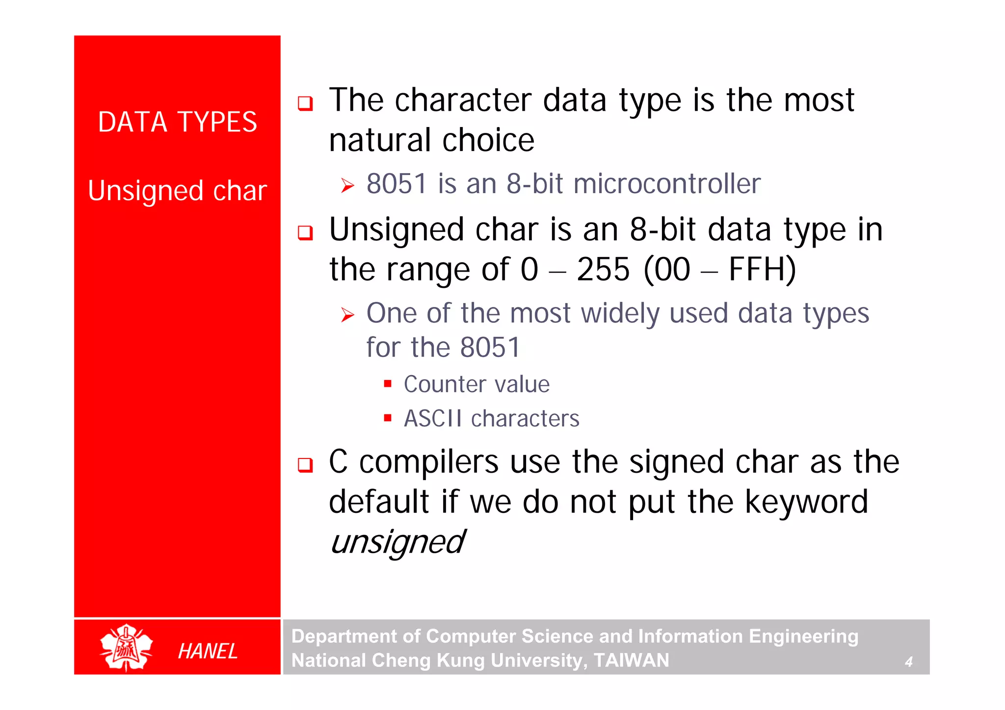
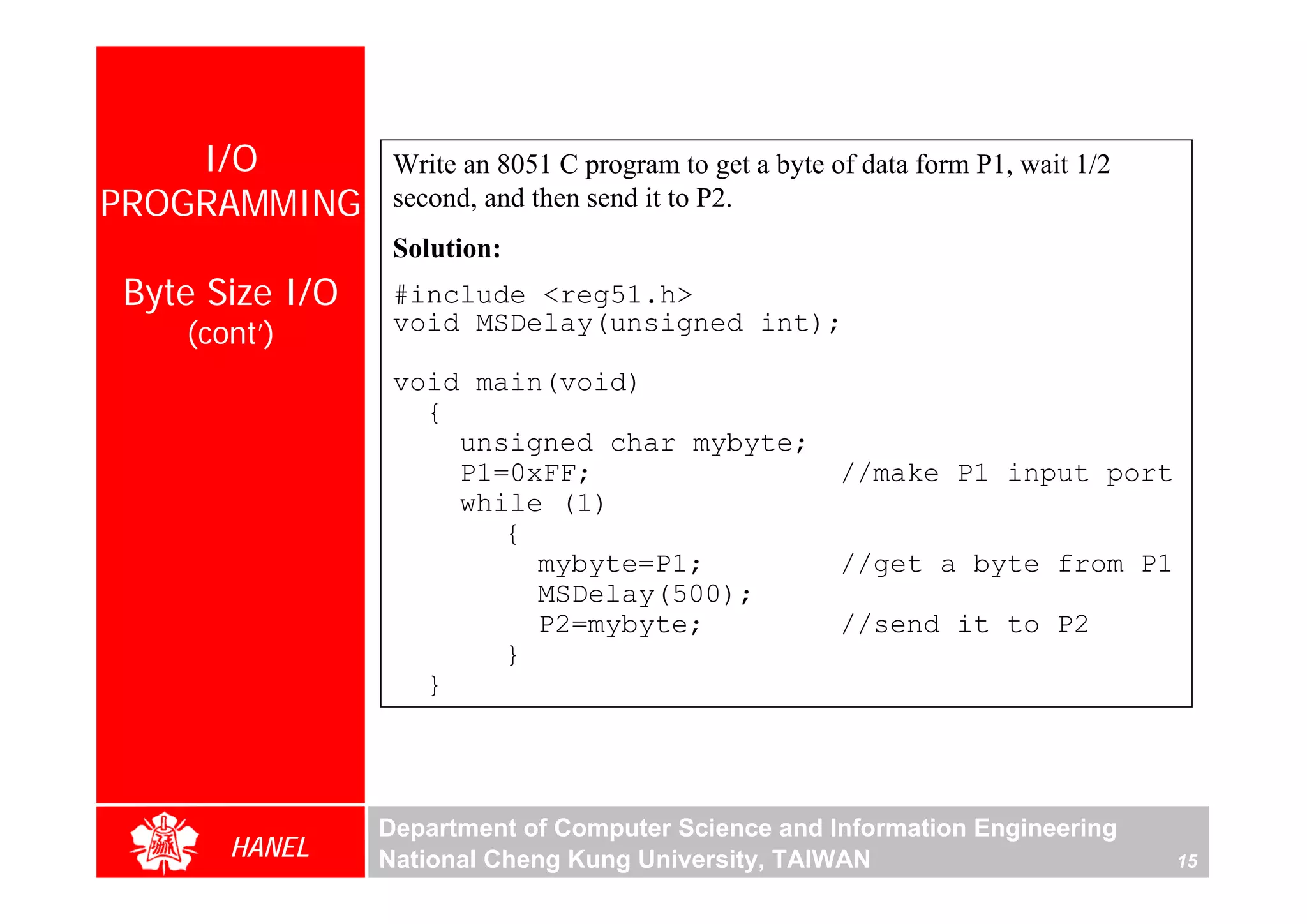
![The signed char is an 8-bit data type
DATA TYPES Use the MSB D7 to represent – or +
Give us values from –128 to +127
Signed char We should stick with the unsigned char
unless the data needs to be
represented as signed numbers
temperature
Write an 8051 C program to send values of –4 to +4 to port P1.
Solution:
//Singed numbers
#include <reg51.h>
void main(void)
{
char mynum[]={+1,-1,+2,-2,+3,-3,+4,-4};
unsigned char z;
for (z=0;z<=8;z++)
P1=mynum[z];
}
Department of Computer Science and Information Engineering
HANEL National Cheng Kung University, TAIWAN 7](https://image.slidesharecdn.com/the8051microcontrollerandembeddedsystemsusingassemblyandc-2nd-ed-120504220416-phpapp02/75/The-8051-microcontroller-and-embedded-systems-using-assembly-and-c-2nd-ed-251-2048.jpg)
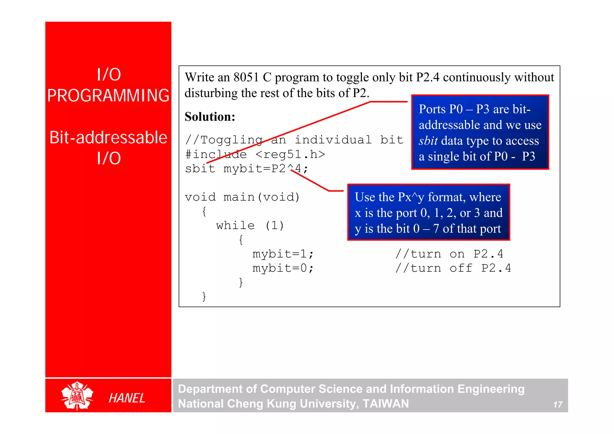
![The data pins of an LCD are connected to P1. The information is
I/O latched into the LCD whenever its Enable pin goes from high to low.
Write an 8051 C program to send “The Earth is but One Country” to
PROGRAMMING this LCD.
Solution:
Bit-addressable #include <reg51.h>
I/O #define LCDData P1 //LCDData declaration
(cont’) sbit En=P2^0; //the enable pin
void main(void)
{
unsigned char message[]
=“The Earth is but One Country”;
unsigned char z;
for (z=0;z<28;z++) //send 28 characters
{
LCDData=message[z];
En=1; //a high-
En=0; //-to-low pulse to latch data
}
}
Department of Computer Science and Information Engineering
HANEL National Cheng Kung University, TAIWAN 20](https://image.slidesharecdn.com/the8051microcontrollerandembeddedsystemsusingassemblyandc-2nd-ed-120504220416-phpapp02/75/The-8051-microcontroller-and-embedded-systems-using-assembly-and-c-2nd-ed-264-2048.jpg)
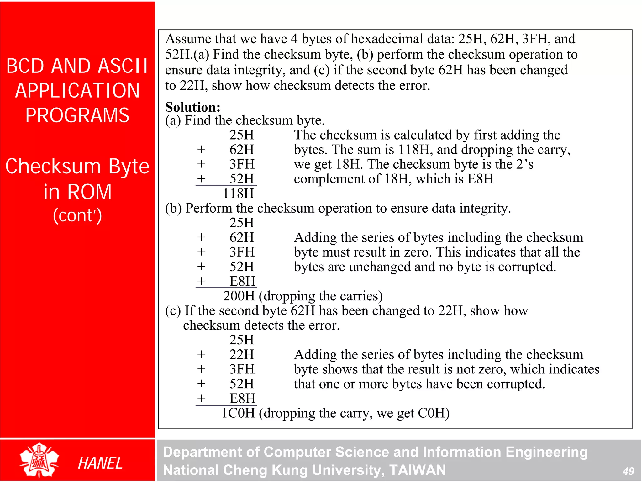
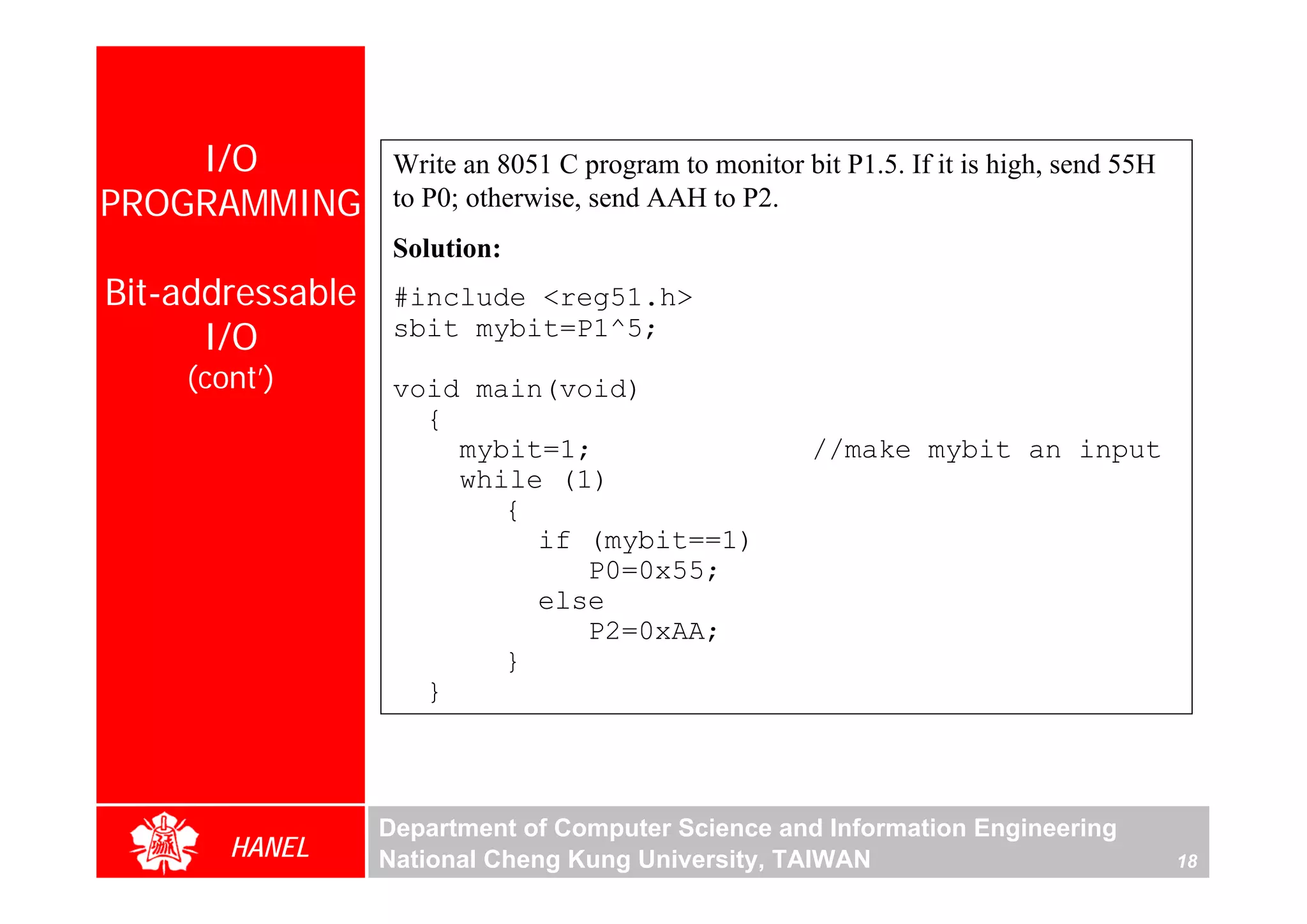
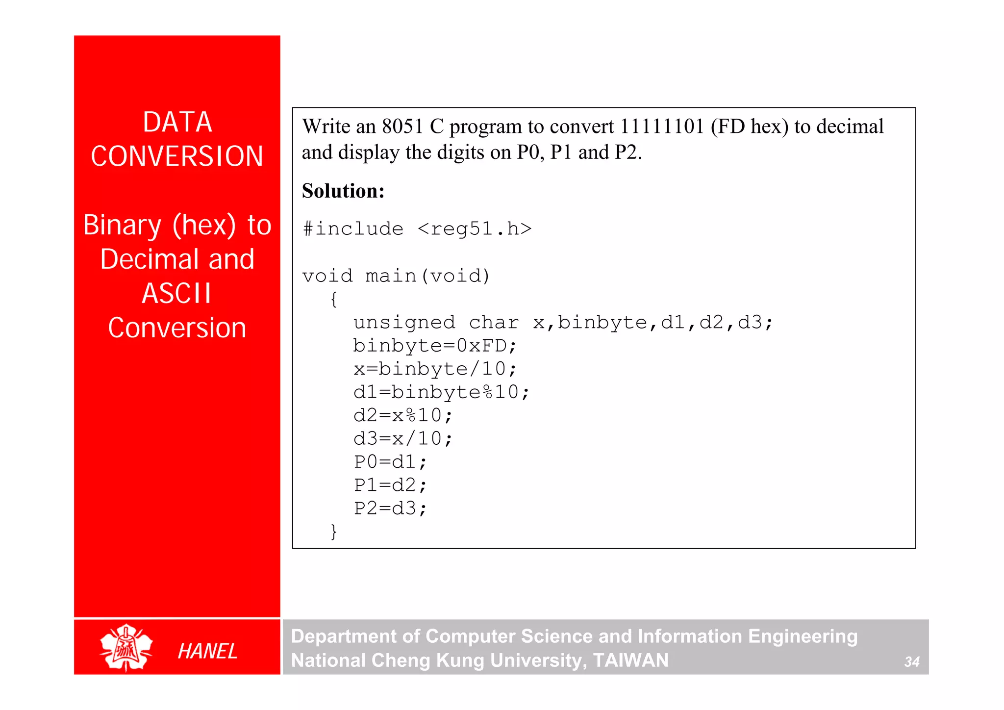
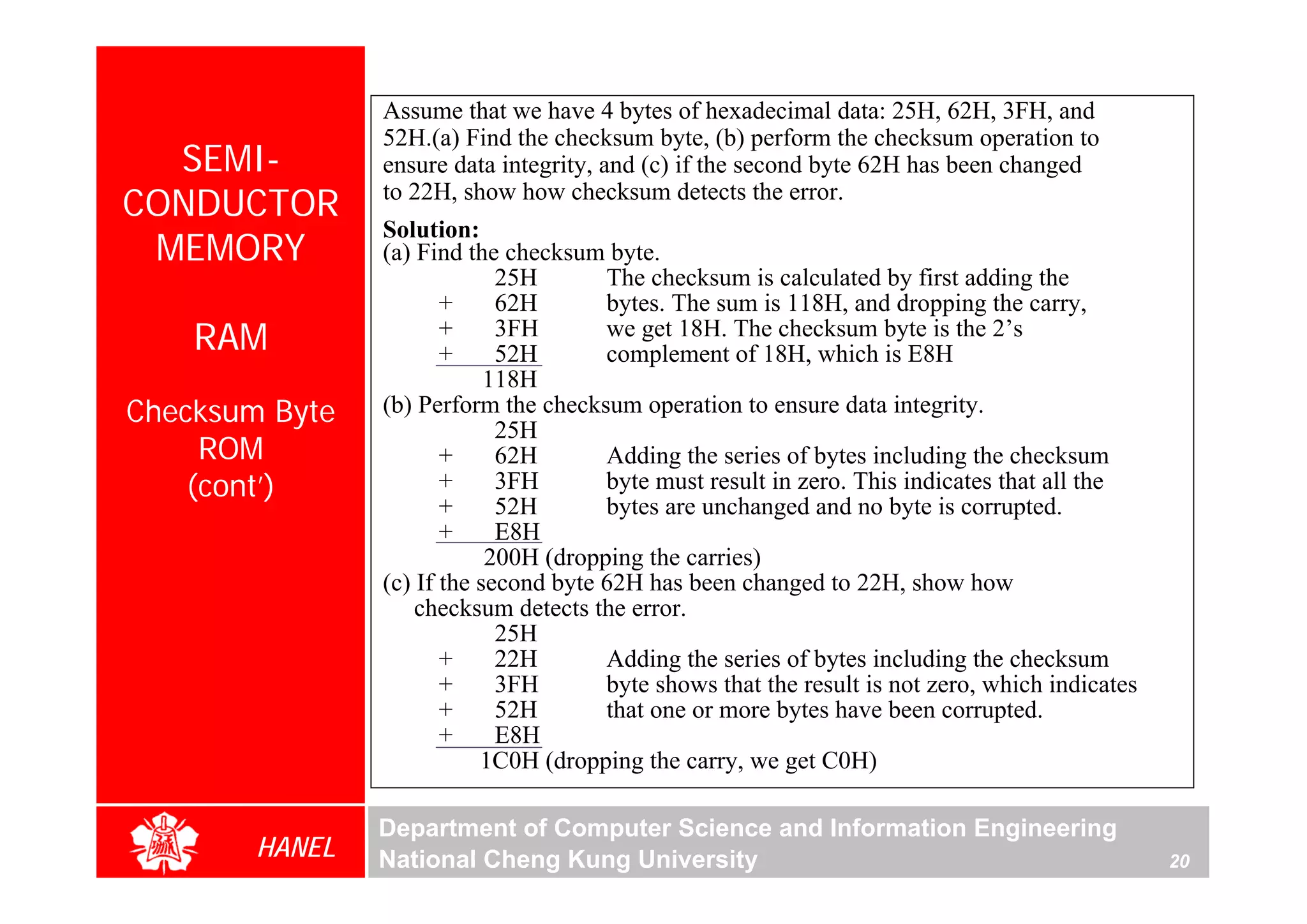
![DATA Write an 8051 C program to calculate the checksum byte for the data
25H, 62H, 3FH, and 52H.
CONVERSION
Solution:
Checksum Byte #include <reg51.h>
in ROM void main(void)
{
unsigned char mydata[]={0x25,0x62,0x3F,0x52};
unsigned char sum=0;
unsigned char x;
unsigned char chksumbyte;
for (x=0;x<4;x++)
{
P2=mydata[x];
sum=sum+mydata[x];
P1=sum;
}
chksumbyte=~sum+1;
P1=chksumbyte;
}
Department of Computer Science and Information Engineering
HANEL National Cheng Kung University, TAIWAN 32](https://image.slidesharecdn.com/the8051microcontrollerandembeddedsystemsusingassemblyandc-2nd-ed-120504220416-phpapp02/75/The-8051-microcontroller-and-embedded-systems-using-assembly-and-c-2nd-ed-276-2048.jpg)
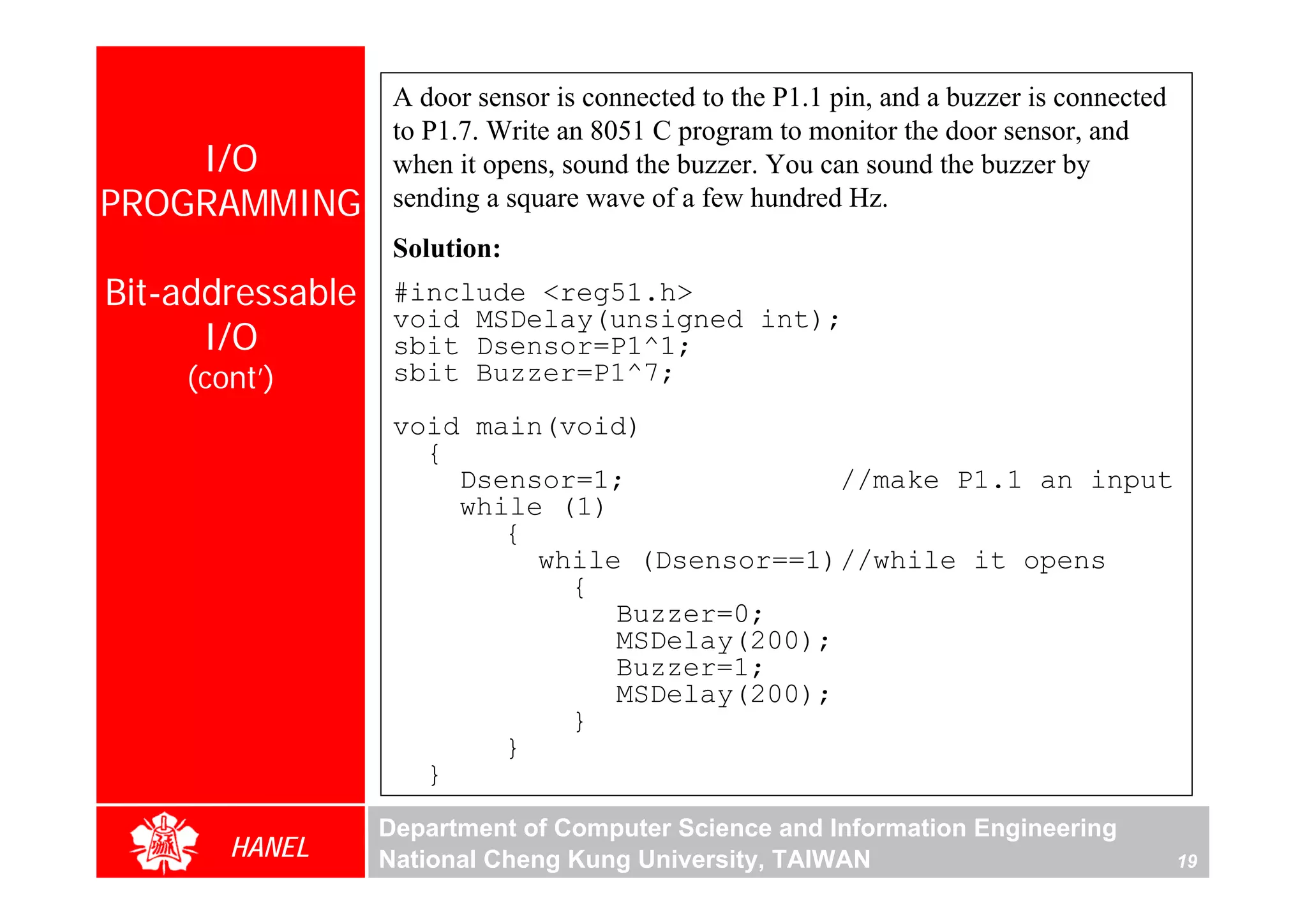
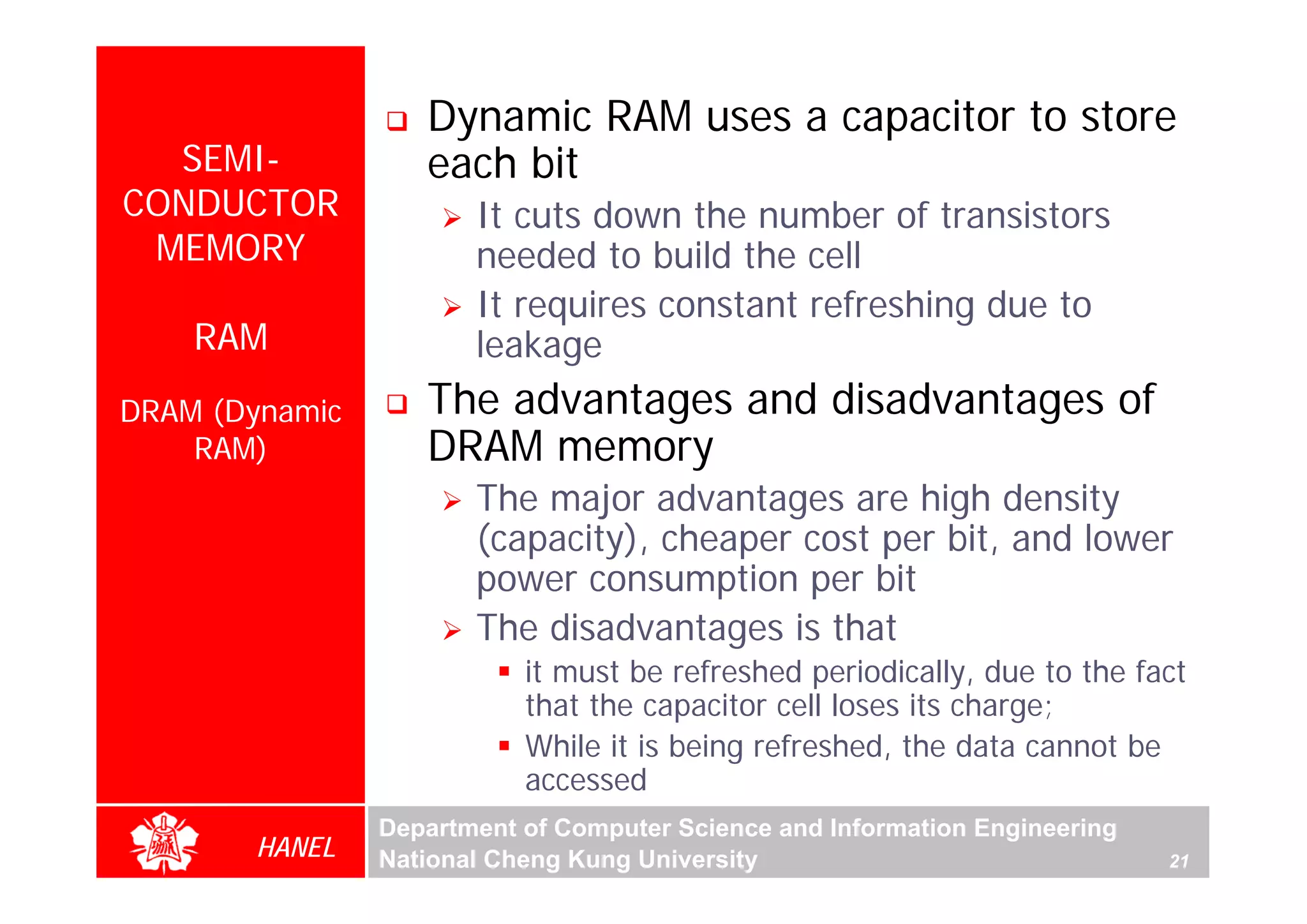
![DATA Write an 8051 C program to perform the checksum operation to
CONVERSION ensure data integrity. If data is good, send ASCII character ‘G’ to P0.
Otherwise send ‘B’ to P0.
Checksum Byte Solution:
in ROM #include <reg51.h>
(cont’) void main(void)
{
unsigned char mydata[]
={0x25,0x62,0x3F,0x52,0xE8};
unsigned char shksum=0;
unsigned char x;
for (x=0;x<5;x++)
chksum=chksum+mydata[x];
if (chksum==0)
P0=‘G’;
else
P0=‘B’;
}
Department of Computer Science and Information Engineering
HANEL National Cheng Kung University, TAIWAN 33](https://image.slidesharecdn.com/the8051microcontrollerandembeddedsystemsusingassemblyandc-2nd-ed-120504220416-phpapp02/75/The-8051-microcontroller-and-embedded-systems-using-assembly-and-c-2nd-ed-277-2048.jpg)
![ACCESSING Compile and single-step the following program on your 8051
CODE ROM simulator. Examine the contents of the 128-byte RAM space to locate
the ASCII values.
RAM Data Solution:
Space Usage #include <reg51.h>
by 8051 C void main(void)
Compiler {
unsigned char mynum[]=“ABCDEF”; //RAM space
(cont’) unsigned char z;
for (z=0;z<=6;z++)
P1=mynum[z];
}
Department of Computer Science and Information Engineering
HANEL National Cheng Kung University, TAIWAN 36](https://image.slidesharecdn.com/the8051microcontrollerandembeddedsystemsusingassemblyandc-2nd-ed-120504220416-phpapp02/75/The-8051-microcontroller-and-embedded-systems-using-assembly-and-c-2nd-ed-280-2048.jpg)
![ACCESSING Write, compile and single-step the following program on your 8051
CODE ROM simulator. Examine the contents of the code space to locate the values.
Solution:
RAM Data #include <reg51.h>
Space Usage void main(void)
by 8051 C {
Compiler unsigned char mydata[100]; //RAM space
unsigned char x,z=0;
(cont’) for (x=0;x<100;x++)
{
z--;
mydata[x]=z;
P1=z;
}
}
Department of Computer Science and Information Engineering
HANEL National Cheng Kung University, TAIWAN 37](https://image.slidesharecdn.com/the8051microcontrollerandembeddedsystemsusingassemblyandc-2nd-ed-120504220416-phpapp02/75/The-8051-microcontroller-and-embedded-systems-using-assembly-and-c-2nd-ed-281-2048.jpg)
![ACCESSING Compile and single-step the following program on your 8051
CODE ROM simulator. Examine the contents of the code space to locate the ASCII
values.
(cont’) To make the C compiler use the
Solution: code space instead of the RAM
#include <reg51.h> space, we need to put the
keyword code in front of the
void main(void) variable declaration
{
code unsigned char mynum[]=“ABCDEF”;
unsigned char z;
for (z=0;z<=6;z++)
P1=mynum[z];
}
Department of Computer Science and Information Engineering
HANEL National Cheng Kung University, TAIWAN 39](https://image.slidesharecdn.com/the8051microcontrollerandembeddedsystemsusingassemblyandc-2nd-ed-120504220416-phpapp02/75/The-8051-microcontroller-and-embedded-systems-using-assembly-and-c-2nd-ed-283-2048.jpg)
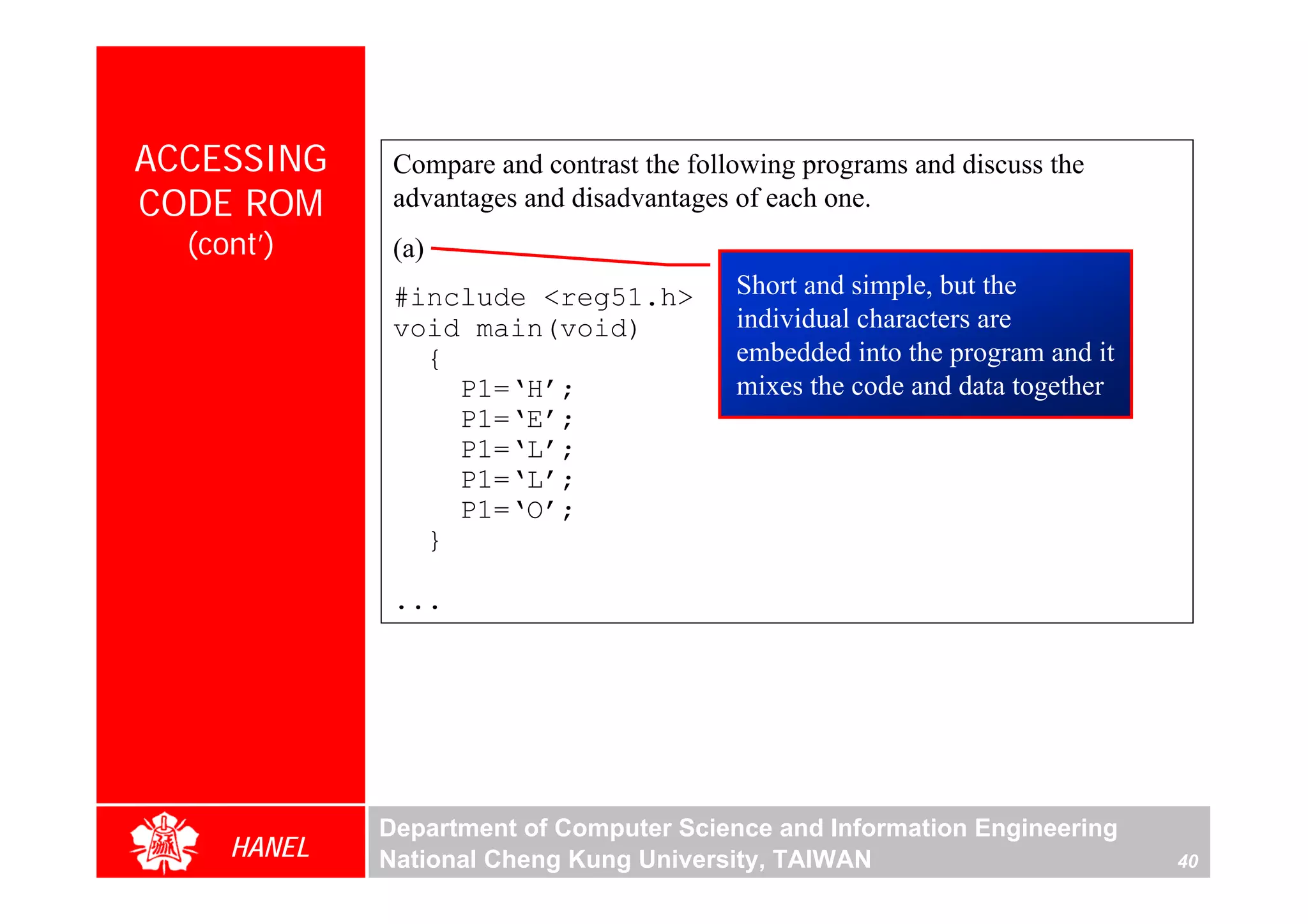
![...
ACCESSING Use the RAM data space to store
CODE ROM (b)
#include <reg51.h>
array elements, therefore the size
(cont’) void main(void) of the array is limited
{
unsigned char mydata[]=“HELLO”;
unsigned char z;
for (z=0;z<=5;z++)
P1=mydata[z]; Use a separate area of the
} code space for data. This
(c) allows the size of the array to
be as long as you want if you
#include <reg51.h>
void main(void) have the on-chip ROM.
{
code unsigned char mydata[]=“HELLO”;
unsigned char z;
for (z=0;z<=5;z++)
P1=mydata[z];
}
However, the more code space you use for data,
the less space is left for your program code
Department of Computer Science and Information Engineering
HANEL National Cheng Kung University, TAIWAN 41](https://image.slidesharecdn.com/the8051microcontrollerandembeddedsystemsusingassemblyandc-2nd-ed-120504220416-phpapp02/75/The-8051-microcontroller-and-embedded-systems-using-assembly-and-c-2nd-ed-285-2048.jpg)


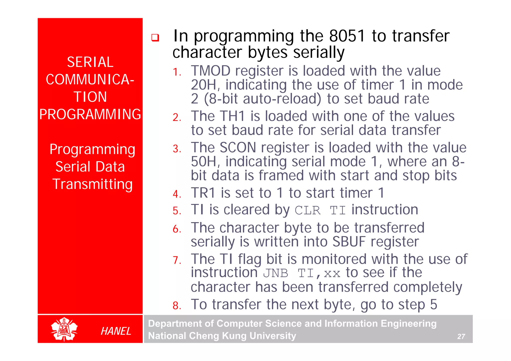
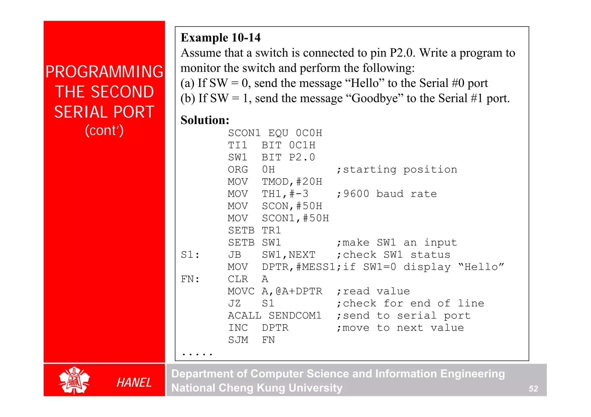
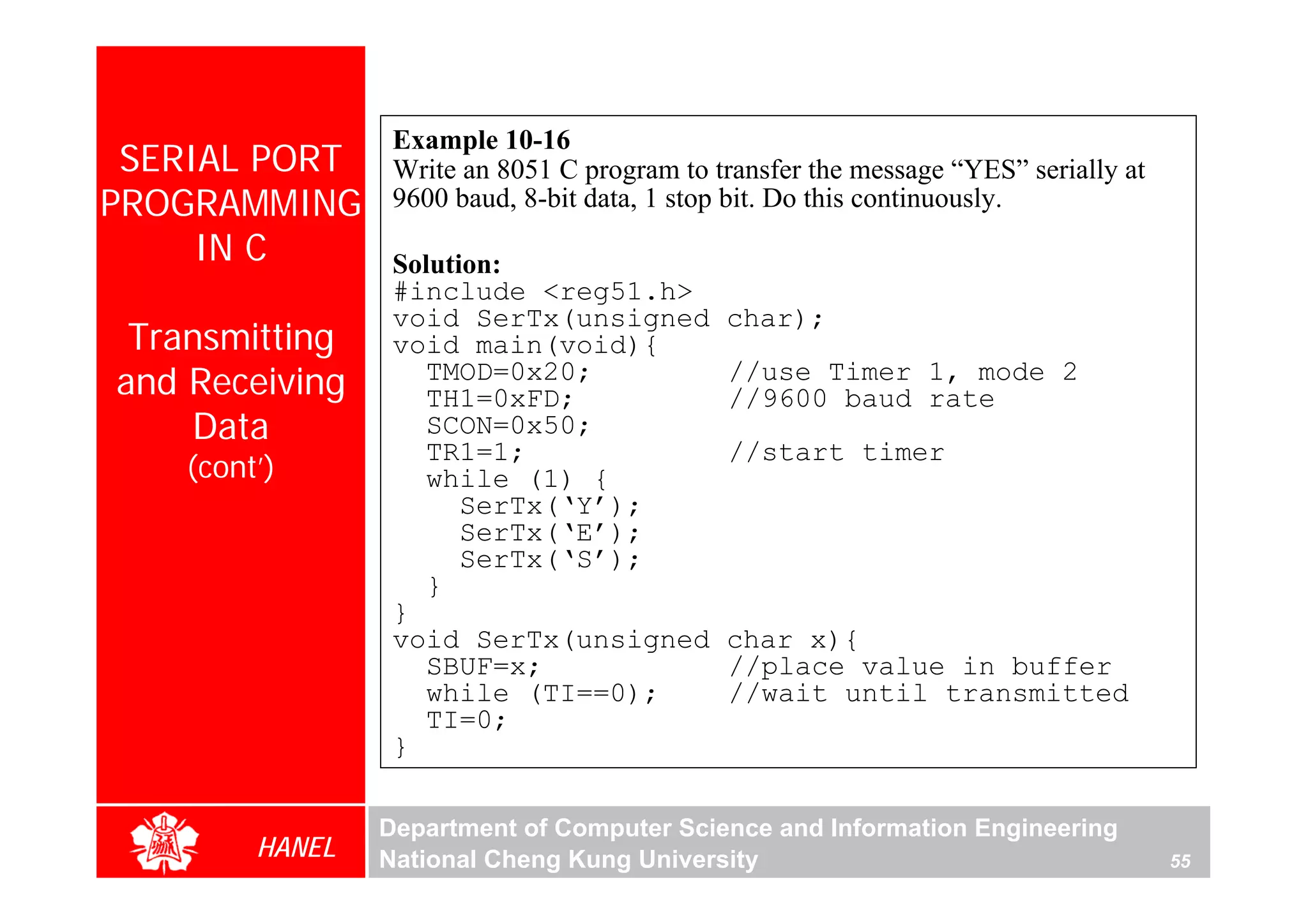
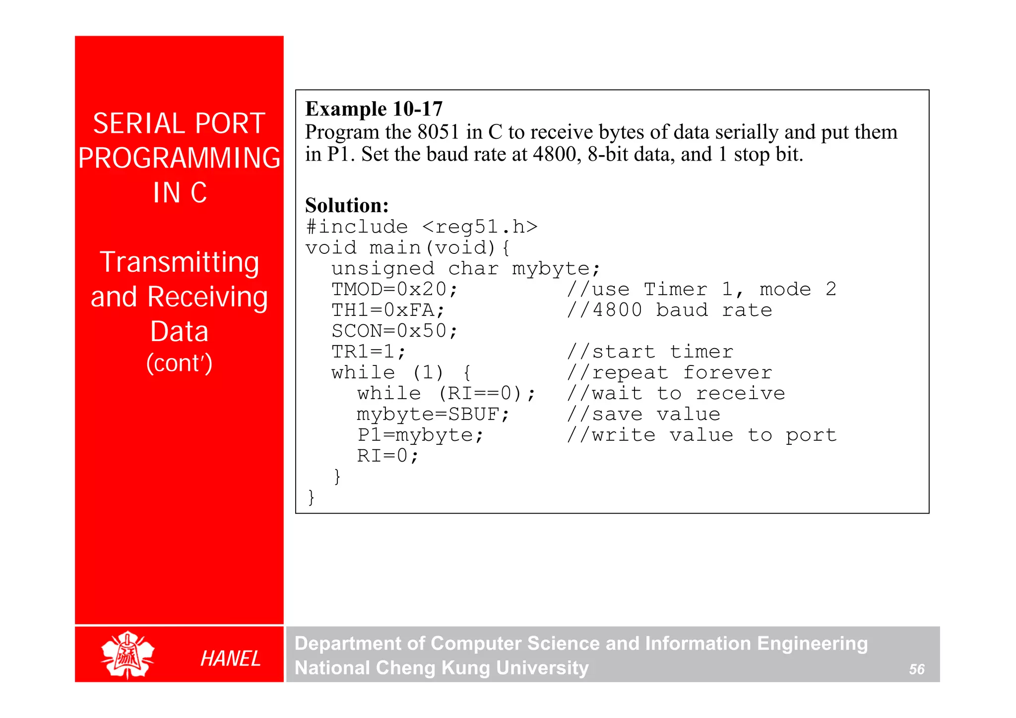
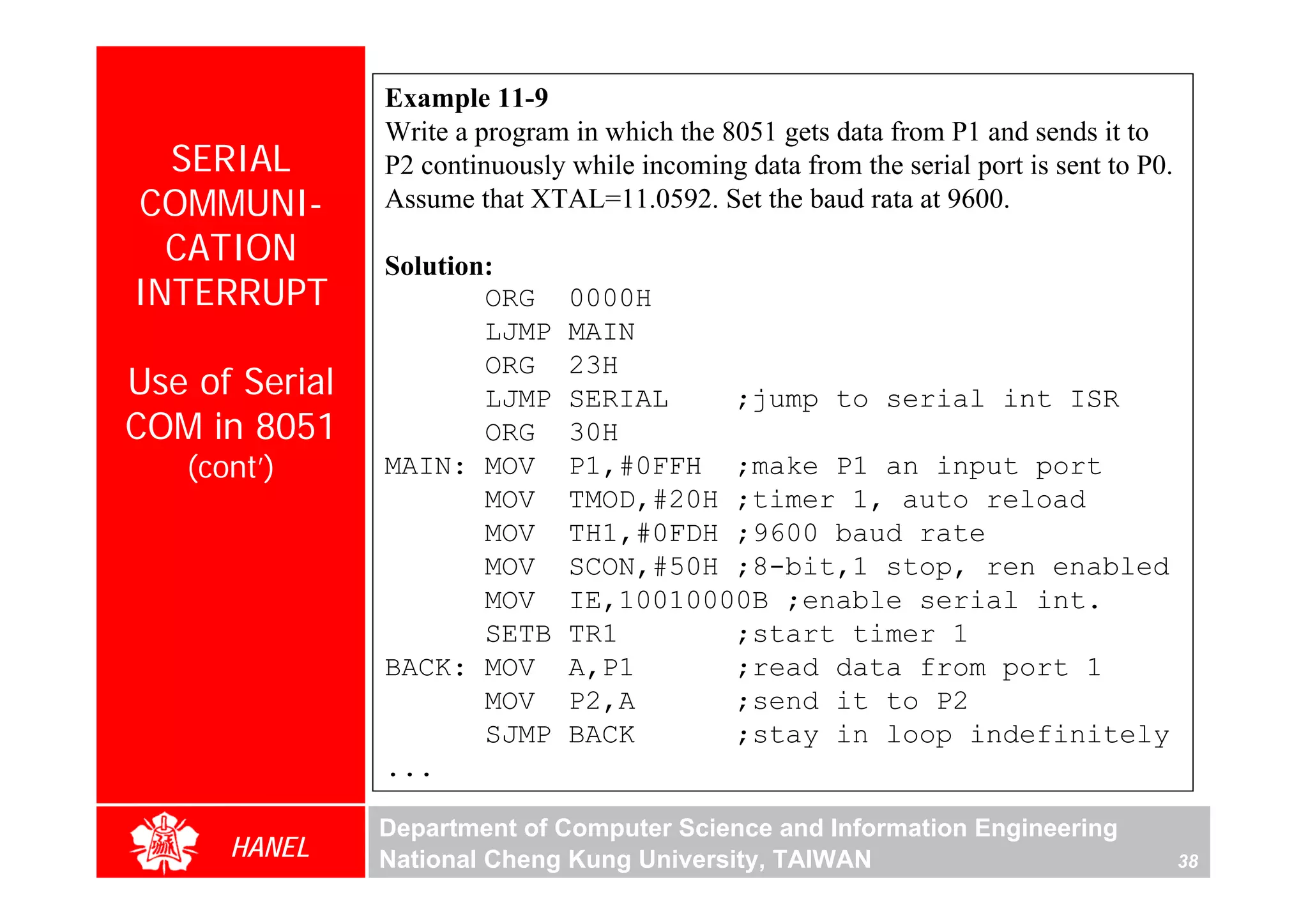
![Example 10-19
SERIAL PORT Write an 8051 C Program to send the two messages “Normal Speed”
PROGRAMMING and “High Speed” to the serial port. Assuming that SW is connected
to pin P2.0, monitor its status and set the baud rate as follows:
IN C SW = 0, 28,800 baud rate
SW = 1, 56K baud rate
Assume that XTAL = 11.0592 MHz for both cases.
Transmitting
and Receiving Solution:
#include <reg51.h>
Data sbit MYSW=P2^0; //input switch
void main(void){
(cont’) unsigned char z;
unsigned char Mess1[]=“Normal Speed”;
unsigned char Mess2[]=“High Speed”;
TMOD=0x20; //use Timer 1, mode 2
TH1=0xFF; //28800 for normal
SCON=0x50;
TR1=1; //start timer
.....
Department of Computer Science and Information Engineering
HANEL National Cheng Kung University 57](https://image.slidesharecdn.com/the8051microcontrollerandembeddedsystemsusingassemblyandc-2nd-ed-120504220416-phpapp02/75/The-8051-microcontroller-and-embedded-systems-using-assembly-and-c-2nd-ed-414-2048.jpg)
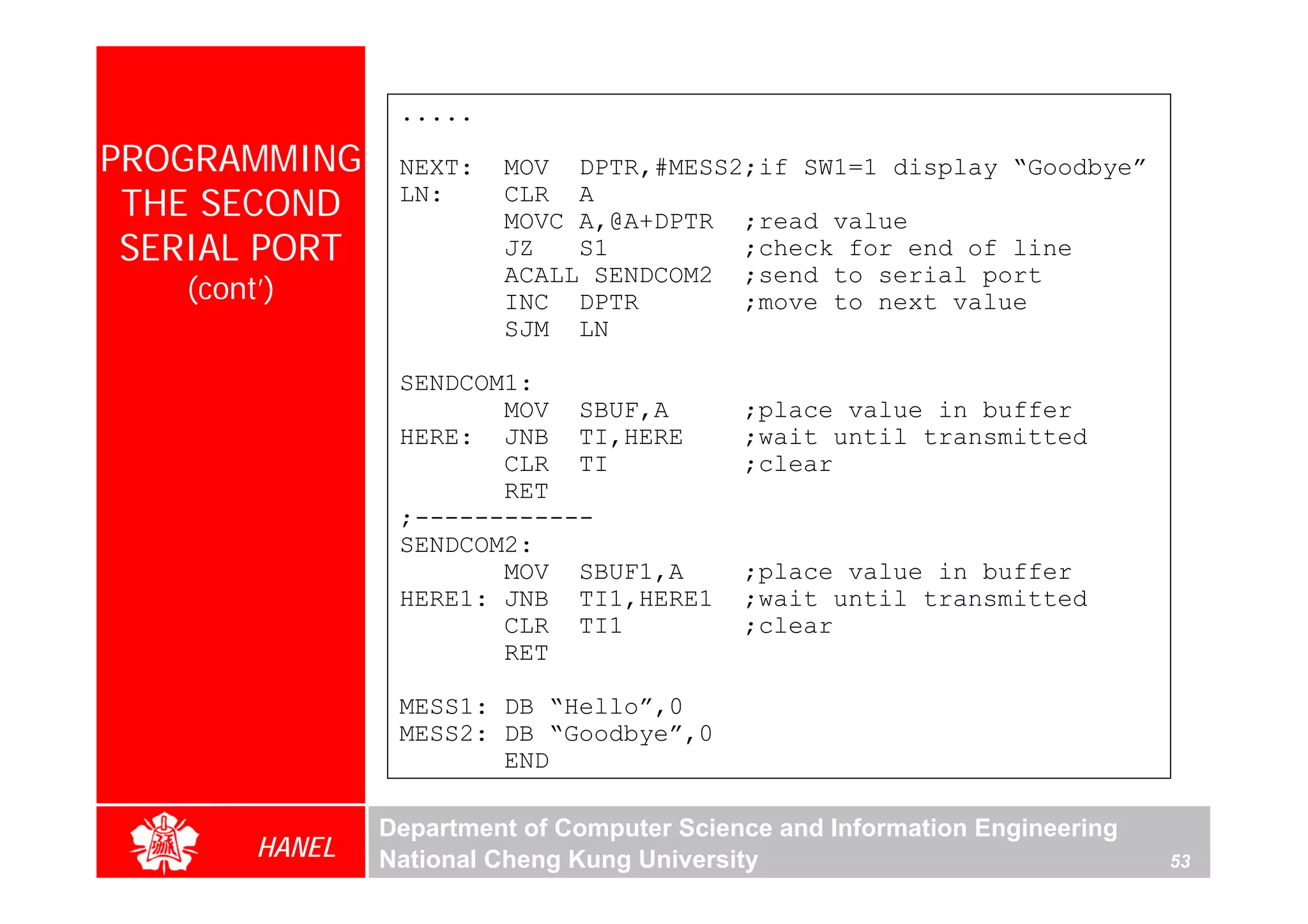
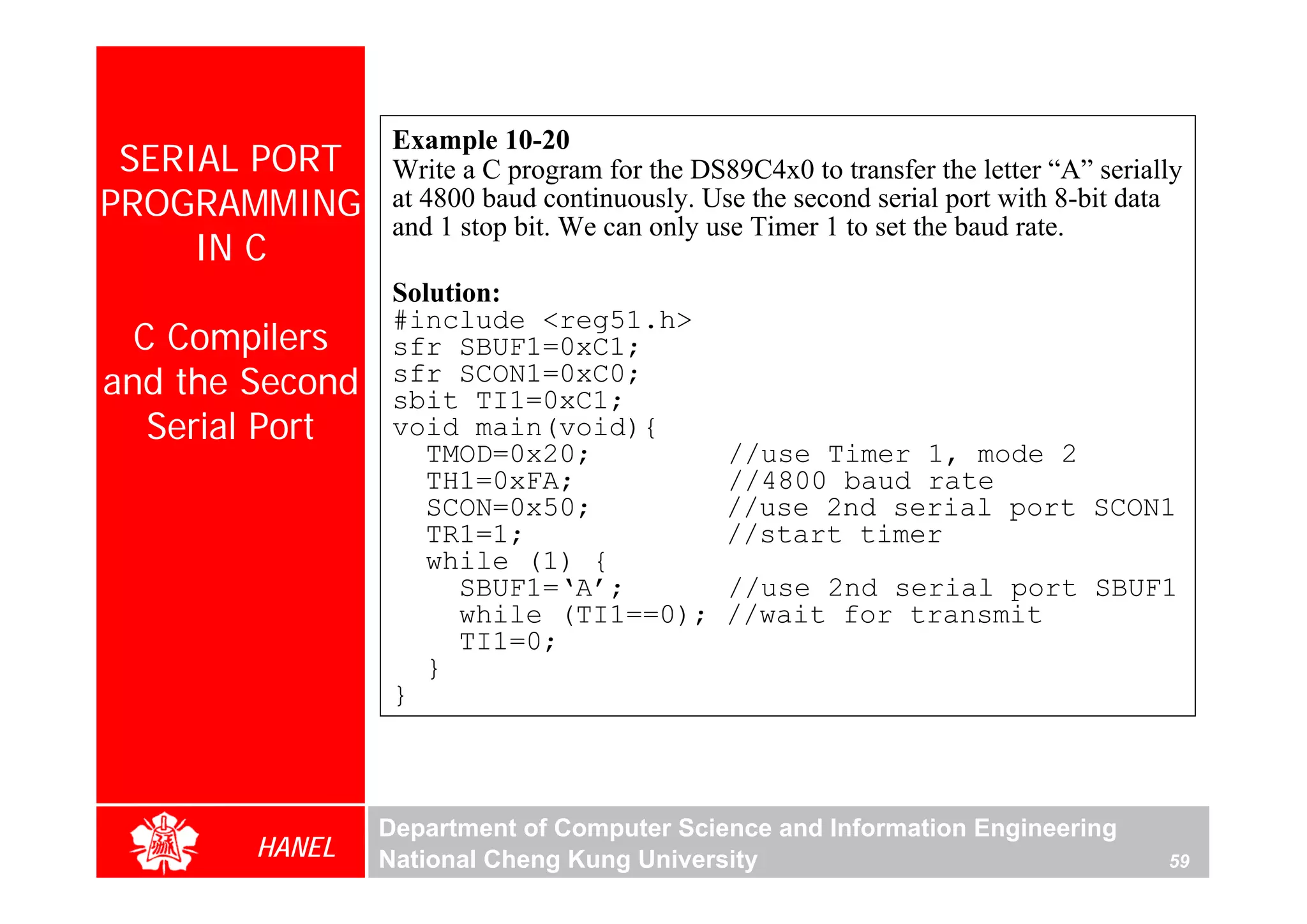
![.....
SERIAL PORT if(MYSW==0) {
PROGRAMMING for (z=0;z<12;z++) {
IN C SBUF=Mess1[z]; //place value in buffer
while(TI==0); //wait for transmit
TI=0;
Transmitting }
and Receiving }
else {
Data PCON=PCON|0x80; //for high speed of 56K
(cont’) for (z=0;z<10;z++) {
SBUF=Mess2[z]; //place value in buffer
while(TI==0); //wait for transmit
TI=0;
}
}
}
Department of Computer Science and Information Engineering
HANEL National Cheng Kung University 58](https://image.slidesharecdn.com/the8051microcontrollerandembeddedsystemsusingassemblyandc-2nd-ed-120504220416-phpapp02/75/The-8051-microcontroller-and-embedded-systems-using-assembly-and-c-2nd-ed-415-2048.jpg)


![An Assembly language instruction
8051
ASSEMBLY consists of four fields:
PROGRAMMING [label:] Mnemonic [operands] [;comment]
ORG 0H ;start(origin) at location
Structure of 0
MOV R5, #25H ;load 25H into R5
Assembly MOV R7, #34H ;load 34H into R7 Directives do not
Language MOV A, #0 ;load 0 into generate any machine
A
ADD A, R5 ;add contents ofand are used
code R5 to A
;now A = A + only by the assembler
R5
Mnemonics ADD A, R7 ;add contents of R7 to A
produce ;now A = A + R7
opcodes ADD A, #12H ;add to A value 12H
;now A = A + 12H
HERE: SJMP HERE ;stay in this loop
END ;end of asm may be at the end of a
Comments source file
The label field allows line or on a line by themselves
the program to refer to a The assembler ignores comments
line of code by name
Department of Computer Science and Information Engineering
HANEL National Cheng Kung University, TAIWAN 10](https://crownmelresort.com/image.slidesharecdn.com/the8051microcontrollerandembeddedsystemsusingassemblyandc-2nd-ed-120504220416-phpapp02/75/The-8051-microcontroller-and-embedded-systems-using-assembly-and-c-2nd-ed-66-2048.jpg)


![Find the size of the delay in following program, if the crystal
TIME DELAY frequency is 11.0592MHz.
FOR VARIOUS
8051 CHIPS MOV A,#55H
AGAIN: MOV P1,A
ACALL DELAY
Delay CPL A
Calculation SJMP AGAIN A simple way to short jump
to itself in order to keep the
;---time delay-------
DELAY: MOV R3,#200 microcontroller busy
HERE: DJNZ R3,HERE HERE: SJMP HERE
RET We can use the following:
SJMP $
Solution:
Machine cycle
DELAY: MOV R3,#200 1
HERE: DJNZ R3,HERE 2
RET 2
Therefore, [(200x2)+1+2]x1.085μs = 436.255μs.
Department of Computer Science and Information Engineering
HANEL National Cheng Kung University, TAIWAN 20](https://crownmelresort.com/image.slidesharecdn.com/the8051microcontrollerandembeddedsystemsusingassemblyandc-2nd-ed-120504220416-phpapp02/75/The-8051-microcontroller-and-embedded-systems-using-assembly-and-c-2nd-ed-123-2048.jpg)
![Find the size of the delay in following program, if the crystal
TIME DELAY frequency is 11.0592MHz.
FOR VARIOUS
8051 CHIPS Machine Cycle
DELAY: MOV R3,#250 1
HERE: NOP 1
Increasing NOP 1
Delay Using NOP 1
NOP 1
NOP DJNZ R3,HERE 2
RET 2
Solution:
The time delay inside HERE loop is
[250(1+1+1+1+2)]x1.085μs = 1627.5μs.
Adding the two instructions outside loop we
have 1627.5μs + 3 x 1.085μs = 1630.755μs
Department of Computer Science and Information Engineering
HANEL National Cheng Kung University, TAIWAN 21](https://crownmelresort.com/image.slidesharecdn.com/the8051microcontrollerandembeddedsystemsusingassemblyandc-2nd-ed-120504220416-phpapp02/75/The-8051-microcontroller-and-embedded-systems-using-assembly-and-c-2nd-ed-124-2048.jpg)


![Write an 8051 C program to send values 00 – FF to port P1.
Solution:
DATA TYPES 1. Pay careful attention to
#include <reg51.h> the size of the data
void main(void) 2. Try to use unsigned char
Unsigned char { instead of int if possible
(cont’) unsigned char z;
for (z=0;z<=255;z++)
P1=z;
}
Write an 8051 C program to send hex values for ASCII characters of
0, 1, 2, 3, 4, 5, A, B, C, and D to port P1.
Solution:
#include <reg51.h>
void main(void)
{
unsigned char mynum[]=“012345ABCD”;
unsigned char z;
for (z=0;z<=10;z++)
P1=mynum[z];
}
Department of Computer Science and Information Engineering
HANEL National Cheng Kung University, TAIWAN 5](https://crownmelresort.com/image.slidesharecdn.com/the8051microcontrollerandembeddedsystemsusingassemblyandc-2nd-ed-120504220416-phpapp02/75/The-8051-microcontroller-and-embedded-systems-using-assembly-and-c-2nd-ed-249-2048.jpg)

![The signed char is an 8-bit data type
DATA TYPES Use the MSB D7 to represent – or +
Give us values from –128 to +127
Signed char We should stick with the unsigned char
unless the data needs to be
represented as signed numbers
temperature
Write an 8051 C program to send values of –4 to +4 to port P1.
Solution:
//Singed numbers
#include <reg51.h>
void main(void)
{
char mynum[]={+1,-1,+2,-2,+3,-3,+4,-4};
unsigned char z;
for (z=0;z<=8;z++)
P1=mynum[z];
}
Department of Computer Science and Information Engineering
HANEL National Cheng Kung University, TAIWAN 7](https://crownmelresort.com/image.slidesharecdn.com/the8051microcontrollerandembeddedsystemsusingassemblyandc-2nd-ed-120504220416-phpapp02/75/The-8051-microcontroller-and-embedded-systems-using-assembly-and-c-2nd-ed-251-2048.jpg)


![The data pins of an LCD are connected to P1. The information is
I/O latched into the LCD whenever its Enable pin goes from high to low.
Write an 8051 C program to send “The Earth is but One Country” to
PROGRAMMING this LCD.
Solution:
Bit-addressable #include <reg51.h>
I/O #define LCDData P1 //LCDData declaration
(cont’) sbit En=P2^0; //the enable pin
void main(void)
{
unsigned char message[]
=“The Earth is but One Country”;
unsigned char z;
for (z=0;z<28;z++) //send 28 characters
{
LCDData=message[z];
En=1; //a high-
En=0; //-to-low pulse to latch data
}
}
Department of Computer Science and Information Engineering
HANEL National Cheng Kung University, TAIWAN 20](https://crownmelresort.com/image.slidesharecdn.com/the8051microcontrollerandembeddedsystemsusingassemblyandc-2nd-ed-120504220416-phpapp02/75/The-8051-microcontroller-and-embedded-systems-using-assembly-and-c-2nd-ed-264-2048.jpg)


![DATA Write an 8051 C program to calculate the checksum byte for the data
25H, 62H, 3FH, and 52H.
CONVERSION
Solution:
Checksum Byte #include <reg51.h>
in ROM void main(void)
{
unsigned char mydata[]={0x25,0x62,0x3F,0x52};
unsigned char sum=0;
unsigned char x;
unsigned char chksumbyte;
for (x=0;x<4;x++)
{
P2=mydata[x];
sum=sum+mydata[x];
P1=sum;
}
chksumbyte=~sum+1;
P1=chksumbyte;
}
Department of Computer Science and Information Engineering
HANEL National Cheng Kung University, TAIWAN 32](https://crownmelresort.com/image.slidesharecdn.com/the8051microcontrollerandembeddedsystemsusingassemblyandc-2nd-ed-120504220416-phpapp02/75/The-8051-microcontroller-and-embedded-systems-using-assembly-and-c-2nd-ed-276-2048.jpg)
![DATA Write an 8051 C program to perform the checksum operation to
CONVERSION ensure data integrity. If data is good, send ASCII character ‘G’ to P0.
Otherwise send ‘B’ to P0.
Checksum Byte Solution:
in ROM #include <reg51.h>
(cont’) void main(void)
{
unsigned char mydata[]
={0x25,0x62,0x3F,0x52,0xE8};
unsigned char shksum=0;
unsigned char x;
for (x=0;x<5;x++)
chksum=chksum+mydata[x];
if (chksum==0)
P0=‘G’;
else
P0=‘B’;
}
Department of Computer Science and Information Engineering
HANEL National Cheng Kung University, TAIWAN 33](https://crownmelresort.com/image.slidesharecdn.com/the8051microcontrollerandembeddedsystemsusingassemblyandc-2nd-ed-120504220416-phpapp02/75/The-8051-microcontroller-and-embedded-systems-using-assembly-and-c-2nd-ed-277-2048.jpg)


![ACCESSING Compile and single-step the following program on your 8051
CODE ROM simulator. Examine the contents of the 128-byte RAM space to locate
the ASCII values.
RAM Data Solution:
Space Usage #include <reg51.h>
by 8051 C void main(void)
Compiler {
unsigned char mynum[]=“ABCDEF”; //RAM space
(cont’) unsigned char z;
for (z=0;z<=6;z++)
P1=mynum[z];
}
Department of Computer Science and Information Engineering
HANEL National Cheng Kung University, TAIWAN 36](https://crownmelresort.com/image.slidesharecdn.com/the8051microcontrollerandembeddedsystemsusingassemblyandc-2nd-ed-120504220416-phpapp02/75/The-8051-microcontroller-and-embedded-systems-using-assembly-and-c-2nd-ed-280-2048.jpg)
![ACCESSING Write, compile and single-step the following program on your 8051
CODE ROM simulator. Examine the contents of the code space to locate the values.
Solution:
RAM Data #include <reg51.h>
Space Usage void main(void)
by 8051 C {
Compiler unsigned char mydata[100]; //RAM space
unsigned char x,z=0;
(cont’) for (x=0;x<100;x++)
{
z--;
mydata[x]=z;
P1=z;
}
}
Department of Computer Science and Information Engineering
HANEL National Cheng Kung University, TAIWAN 37](https://crownmelresort.com/image.slidesharecdn.com/the8051microcontrollerandembeddedsystemsusingassemblyandc-2nd-ed-120504220416-phpapp02/75/The-8051-microcontroller-and-embedded-systems-using-assembly-and-c-2nd-ed-281-2048.jpg)

![ACCESSING Compile and single-step the following program on your 8051
CODE ROM simulator. Examine the contents of the code space to locate the ASCII
values.
(cont’) To make the C compiler use the
Solution: code space instead of the RAM
#include <reg51.h> space, we need to put the
keyword code in front of the
void main(void) variable declaration
{
code unsigned char mynum[]=“ABCDEF”;
unsigned char z;
for (z=0;z<=6;z++)
P1=mynum[z];
}
Department of Computer Science and Information Engineering
HANEL National Cheng Kung University, TAIWAN 39](https://crownmelresort.com/image.slidesharecdn.com/the8051microcontrollerandembeddedsystemsusingassemblyandc-2nd-ed-120504220416-phpapp02/75/The-8051-microcontroller-and-embedded-systems-using-assembly-and-c-2nd-ed-283-2048.jpg)

![...
ACCESSING Use the RAM data space to store
CODE ROM (b)
#include <reg51.h>
array elements, therefore the size
(cont’) void main(void) of the array is limited
{
unsigned char mydata[]=“HELLO”;
unsigned char z;
for (z=0;z<=5;z++)
P1=mydata[z]; Use a separate area of the
} code space for data. This
(c) allows the size of the array to
be as long as you want if you
#include <reg51.h>
void main(void) have the on-chip ROM.
{
code unsigned char mydata[]=“HELLO”;
unsigned char z;
for (z=0;z<=5;z++)
P1=mydata[z];
}
However, the more code space you use for data,
the less space is left for your program code
Department of Computer Science and Information Engineering
HANEL National Cheng Kung University, TAIWAN 41](https://crownmelresort.com/image.slidesharecdn.com/the8051microcontrollerandembeddedsystemsusingassemblyandc-2nd-ed-120504220416-phpapp02/75/The-8051-microcontroller-and-embedded-systems-using-assembly-and-c-2nd-ed-285-2048.jpg)


![Example 10-19
SERIAL PORT Write an 8051 C Program to send the two messages “Normal Speed”
PROGRAMMING and “High Speed” to the serial port. Assuming that SW is connected
to pin P2.0, monitor its status and set the baud rate as follows:
IN C SW = 0, 28,800 baud rate
SW = 1, 56K baud rate
Assume that XTAL = 11.0592 MHz for both cases.
Transmitting
and Receiving Solution:
#include <reg51.h>
Data sbit MYSW=P2^0; //input switch
void main(void){
(cont’) unsigned char z;
unsigned char Mess1[]=“Normal Speed”;
unsigned char Mess2[]=“High Speed”;
TMOD=0x20; //use Timer 1, mode 2
TH1=0xFF; //28800 for normal
SCON=0x50;
TR1=1; //start timer
.....
Department of Computer Science and Information Engineering
HANEL National Cheng Kung University 57](https://crownmelresort.com/image.slidesharecdn.com/the8051microcontrollerandembeddedsystemsusingassemblyandc-2nd-ed-120504220416-phpapp02/75/The-8051-microcontroller-and-embedded-systems-using-assembly-and-c-2nd-ed-414-2048.jpg)
![.....
SERIAL PORT if(MYSW==0) {
PROGRAMMING for (z=0;z<12;z++) {
IN C SBUF=Mess1[z]; //place value in buffer
while(TI==0); //wait for transmit
TI=0;
Transmitting }
and Receiving }
else {
Data PCON=PCON|0x80; //for high speed of 56K
(cont’) for (z=0;z<10;z++) {
SBUF=Mess2[z]; //place value in buffer
while(TI==0); //wait for transmit
TI=0;
}
}
}
Department of Computer Science and Information Engineering
HANEL National Cheng Kung University 58](https://crownmelresort.com/image.slidesharecdn.com/the8051microcontrollerandembeddedsystemsusingassemblyandc-2nd-ed-120504220416-phpapp02/75/The-8051-microcontroller-and-embedded-systems-using-assembly-and-c-2nd-ed-415-2048.jpg)


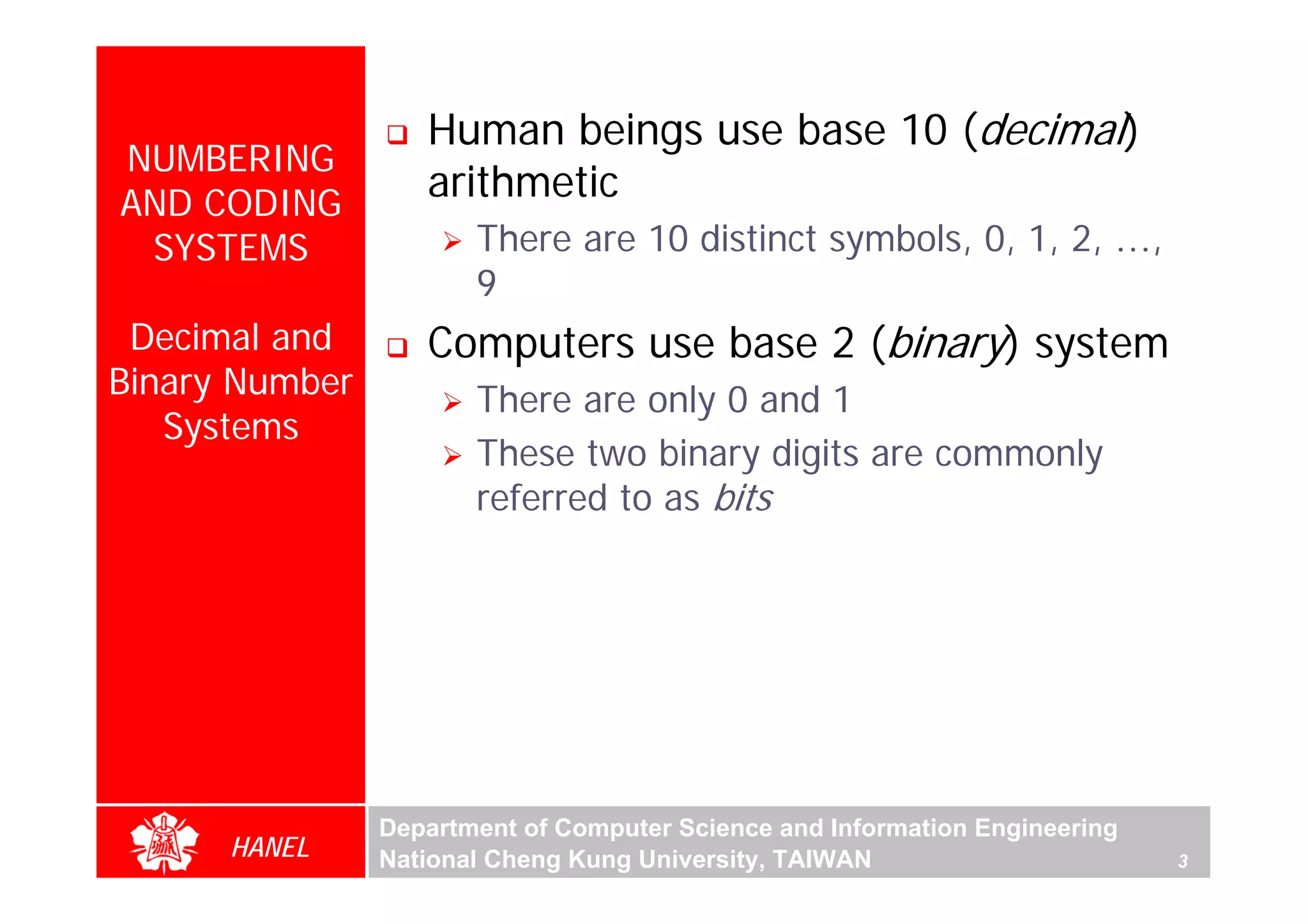
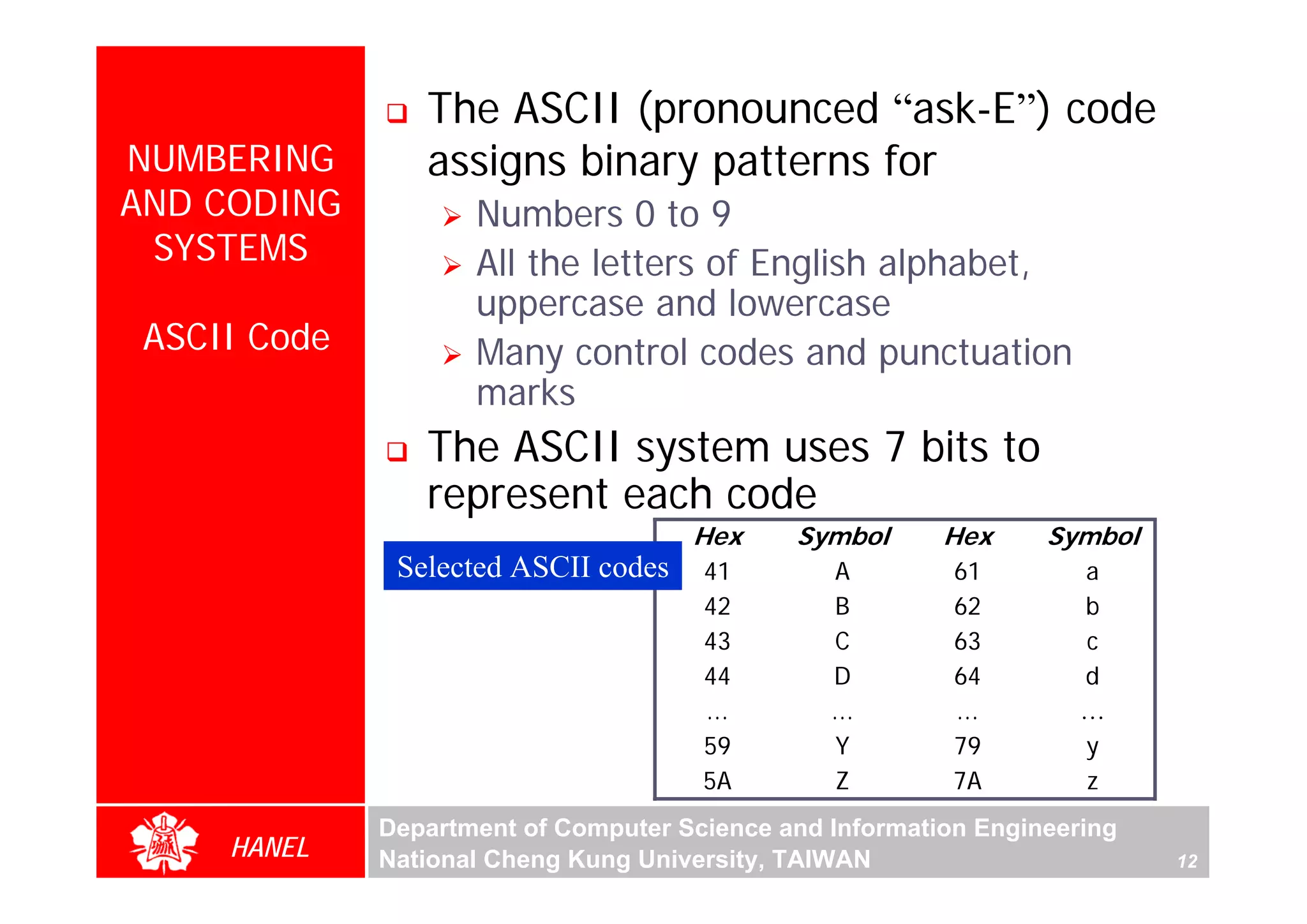
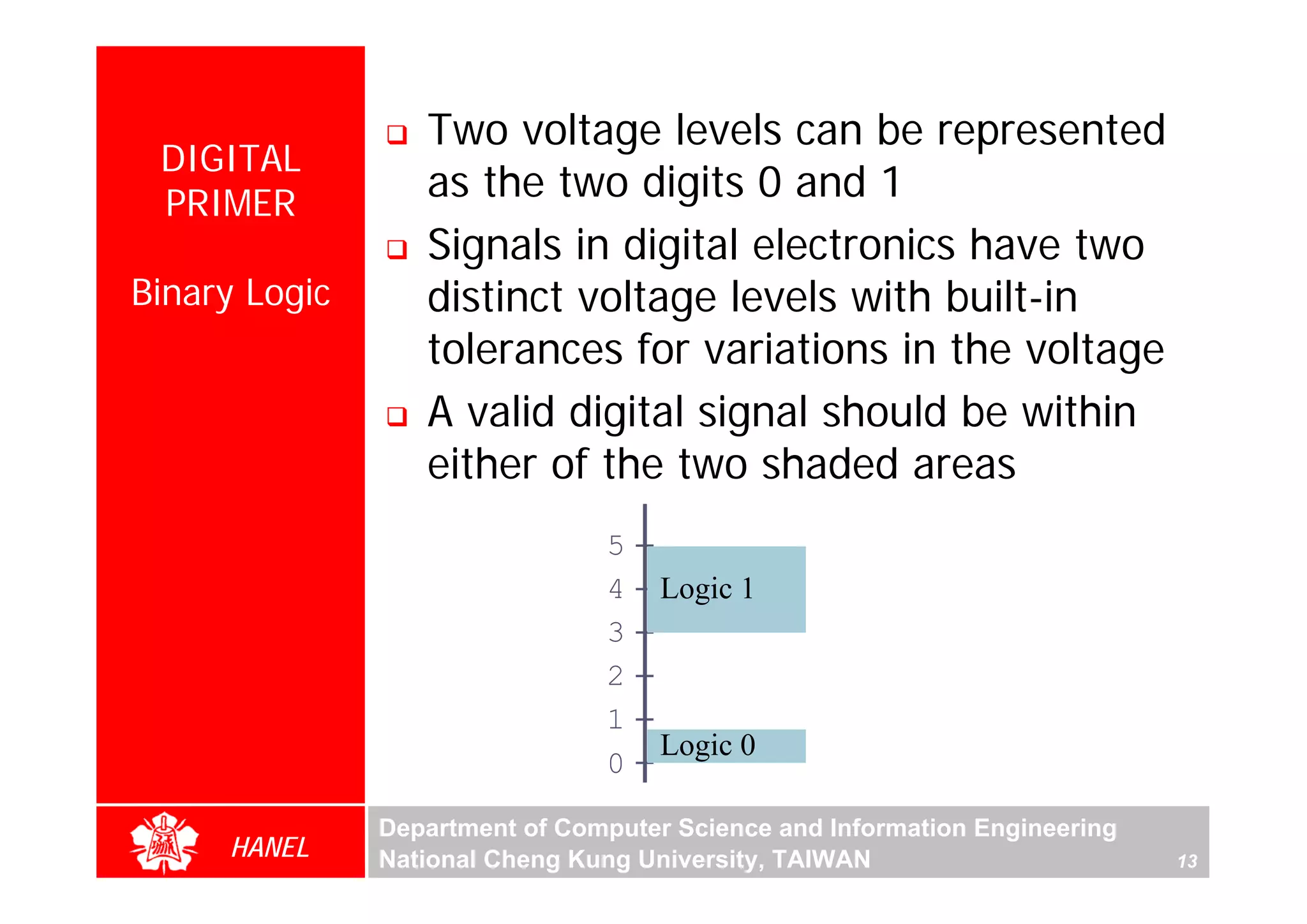
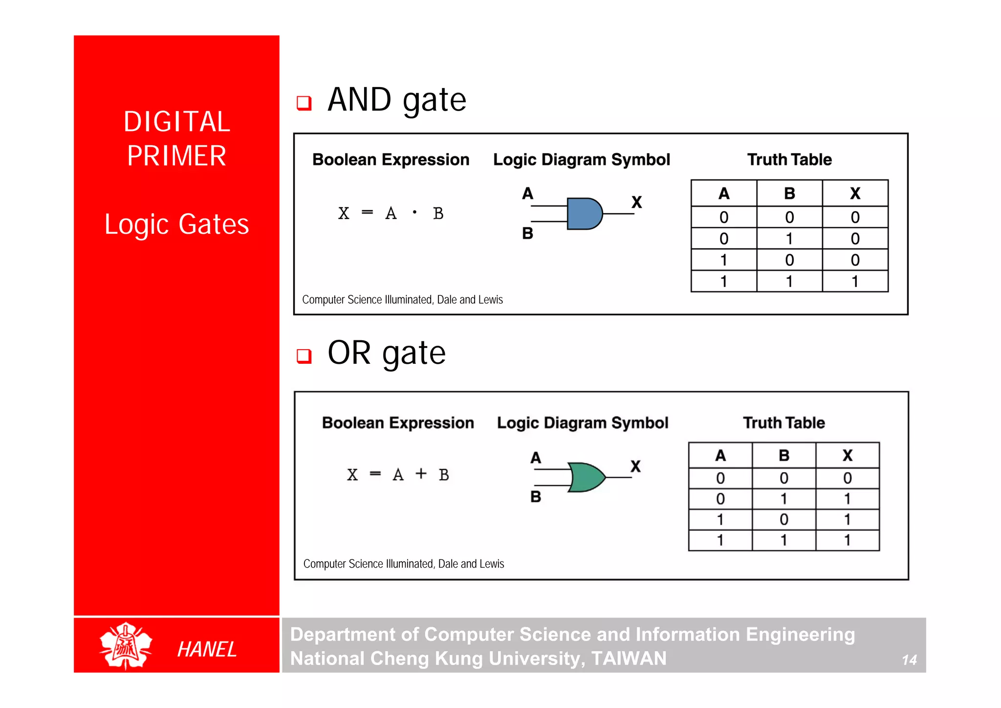
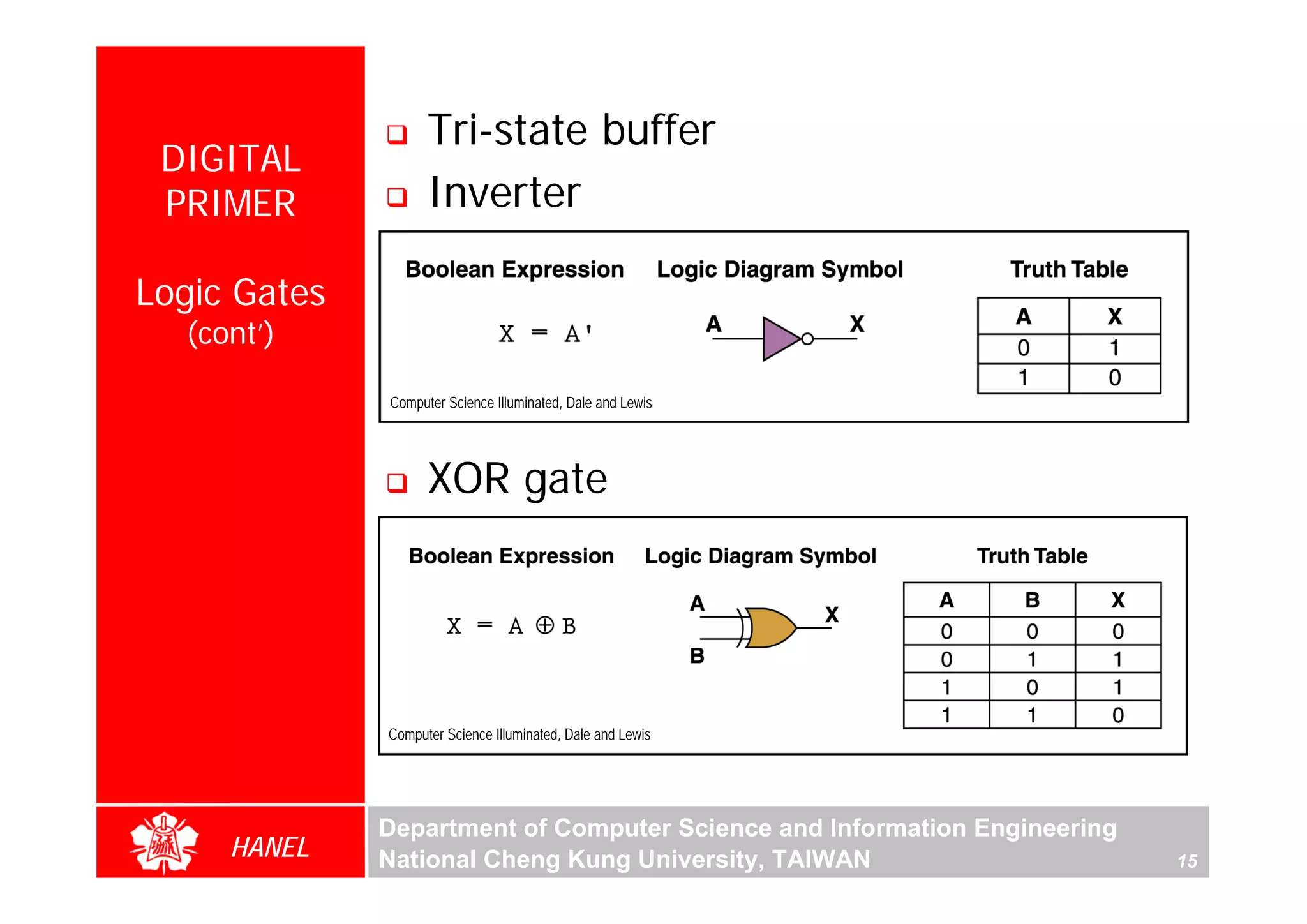
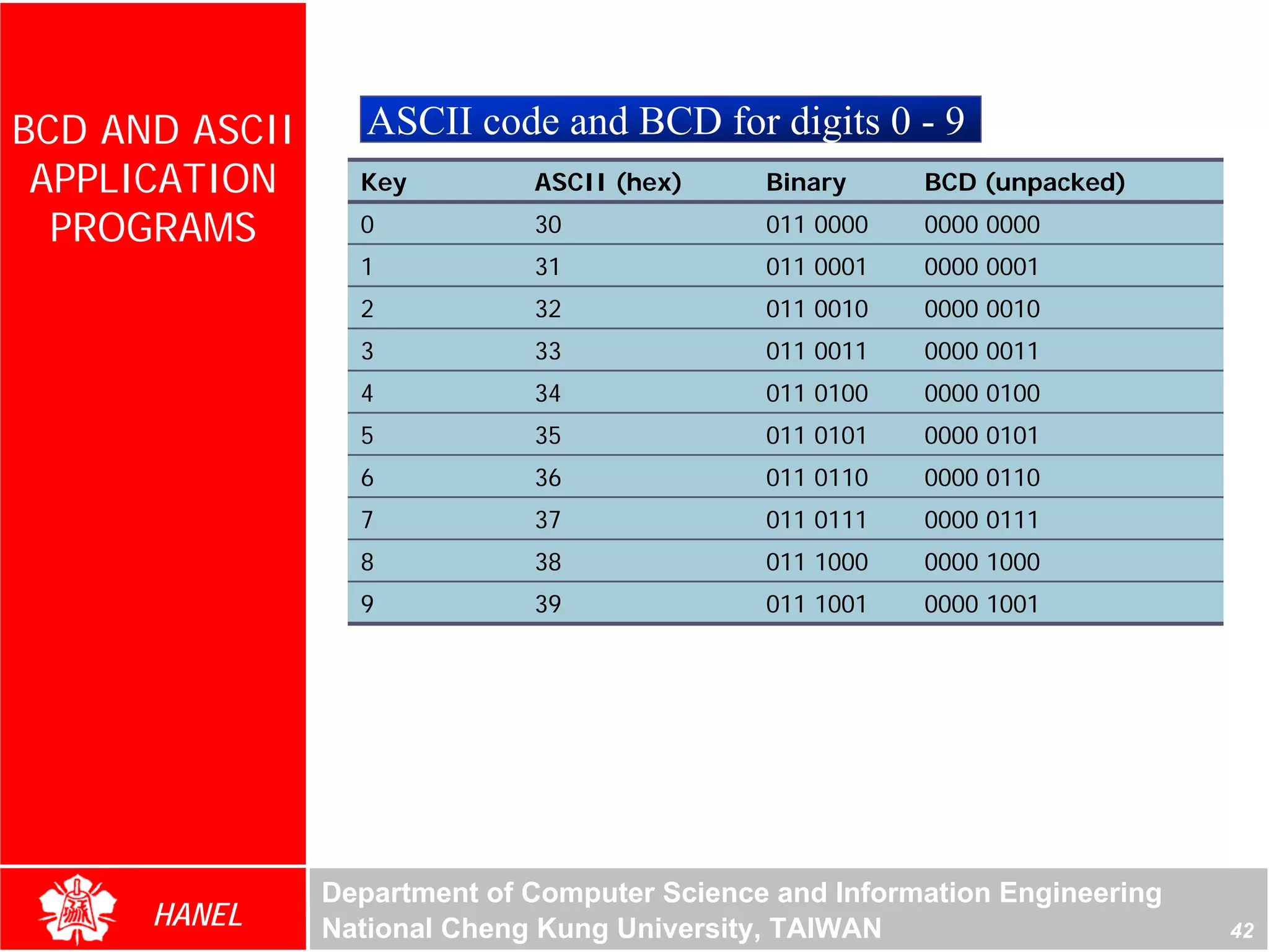
The document is a chapter from the textbook "The 8051 Microcontroller and Embedded Systems: Using Assembly and C" by Muhammad Ali Mazidi, Janice Gillispie Mazidi, and Rolin D. McKinlay. The chapter discusses numbering and coding systems such as binary, decimal, hexadecimal and their conversions. It also covers addition, subtraction and the ASCII code system.


![SHS_Core_CAE_Q3_LE1 FOR THIRD [FINAL].pdf](https://cdn.slidesharecdn.com/ss_thumbnails/shscorecaeq3le1final-251116055110-e3081055-thumbnail.jpg?width=640&height=640&fit=bounds)


