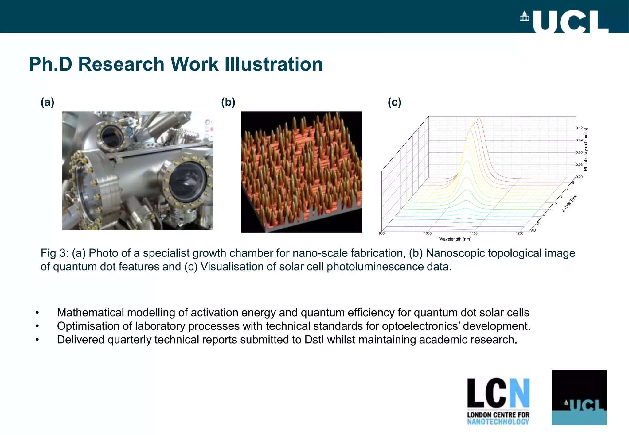
Ph.D Research Work Illustration
• Mathematical modelling of activation energy and quantum efficiency for quantum dot solar cells
• Optimisation of laboratory processes with technical standards for optoelectronics’ development.
• Delivered quarterly technical reports submitted to Dstl whilst maintaining academic research.
900 1000 1100 1200
0.00
0.03
0.06
0.09
0.12
B
F
J
N
P
T
X
AD
Wavelength (nm)
PLIntensity(arb.units)
Z
Axis
Title
(a) (b) (c)
Fig 3: (a) Photo of a specialist growth chamber for nano-scale fabrication, (b) Nanoscopic topological image
of quantum dot features and (c) Visualisation of solar cell photoluminescence data.

LinkedIn Slide presentation_DSTL_179

  • 1.
    Ph.D Research WorkIllustration • Mathematical modelling of activation energy and quantum efficiency for quantum dot solar cells • Optimisation of laboratory processes with technical standards for optoelectronics’ development. • Delivered quarterly technical reports submitted to Dstl whilst maintaining academic research. 900 1000 1100 1200 0.00 0.03 0.06 0.09 0.12 B F J N P T X AD Wavelength (nm) PLIntensity(arb.units) Z Axis Title (a) (b) (c) Fig 3: (a) Photo of a specialist growth chamber for nano-scale fabrication, (b) Nanoscopic topological image of quantum dot features and (c) Visualisation of solar cell photoluminescence data.

Editor's Notes

  • #2 There are three processes throughout the entire investigation for each quantum dot solar cell project. We growth the materials on the substrate wafer. The device structure is the commonly used p-i-n junction, including quantum dots. We can grow different types of quantum dots based on our study. We develop them into workable devices using basic photolithography procedures. We characterise the devices using the available apparatus that we have. They include photoluminesnce, atomic force microscopy, light JV measurements and external quantum efficiency.