Download to read offline


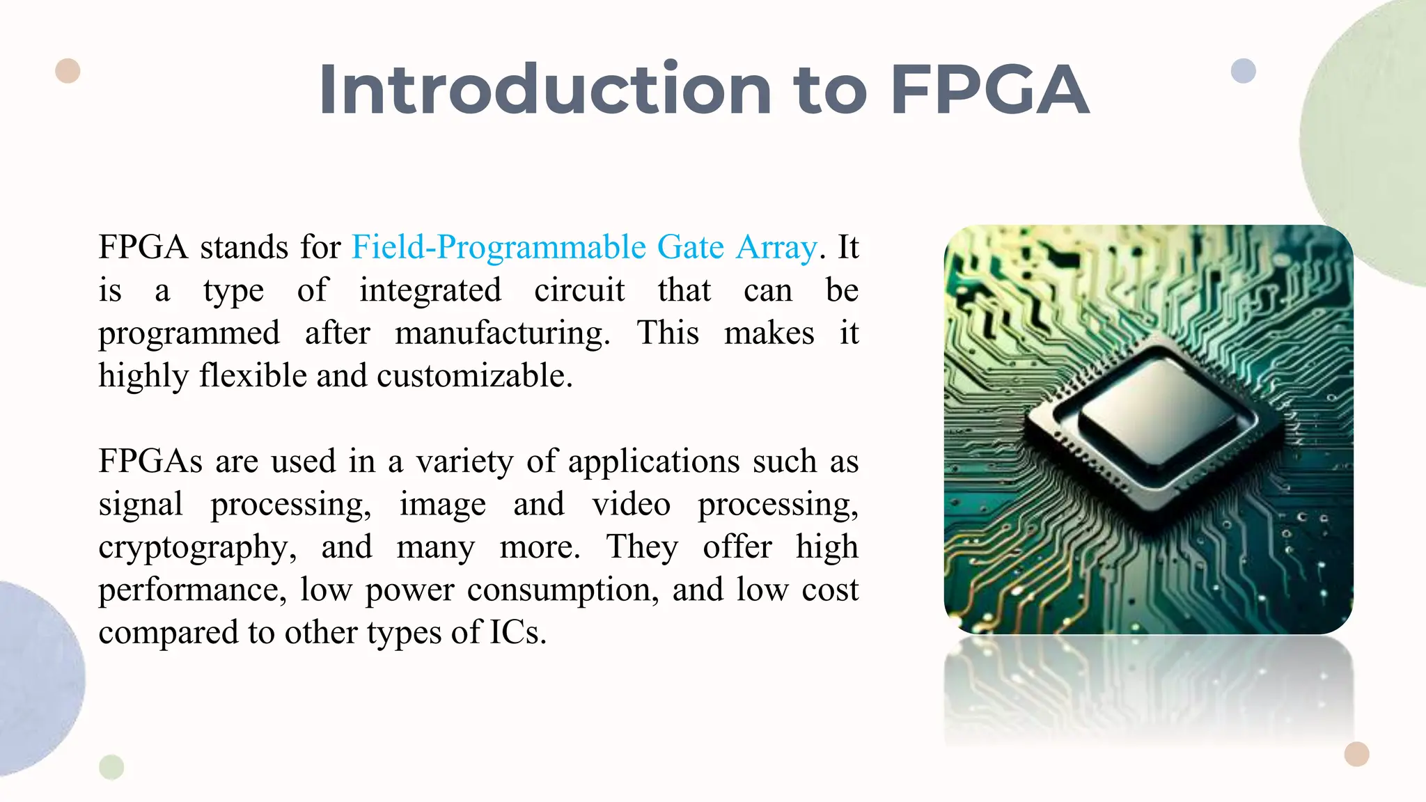


The document provides an overview of field-programmable gate arrays (FPGAs) and the VLSI design flow using hardware description languages (HDLs). It discusses various synthesis processes including behavioral, logic, and physical synthesis, emphasizing their importance in creating efficient and optimized digital circuits. The text highlights the flexibility, performance, and cost-effectiveness of FPGAs and VLSI technologies in modern electronic design.