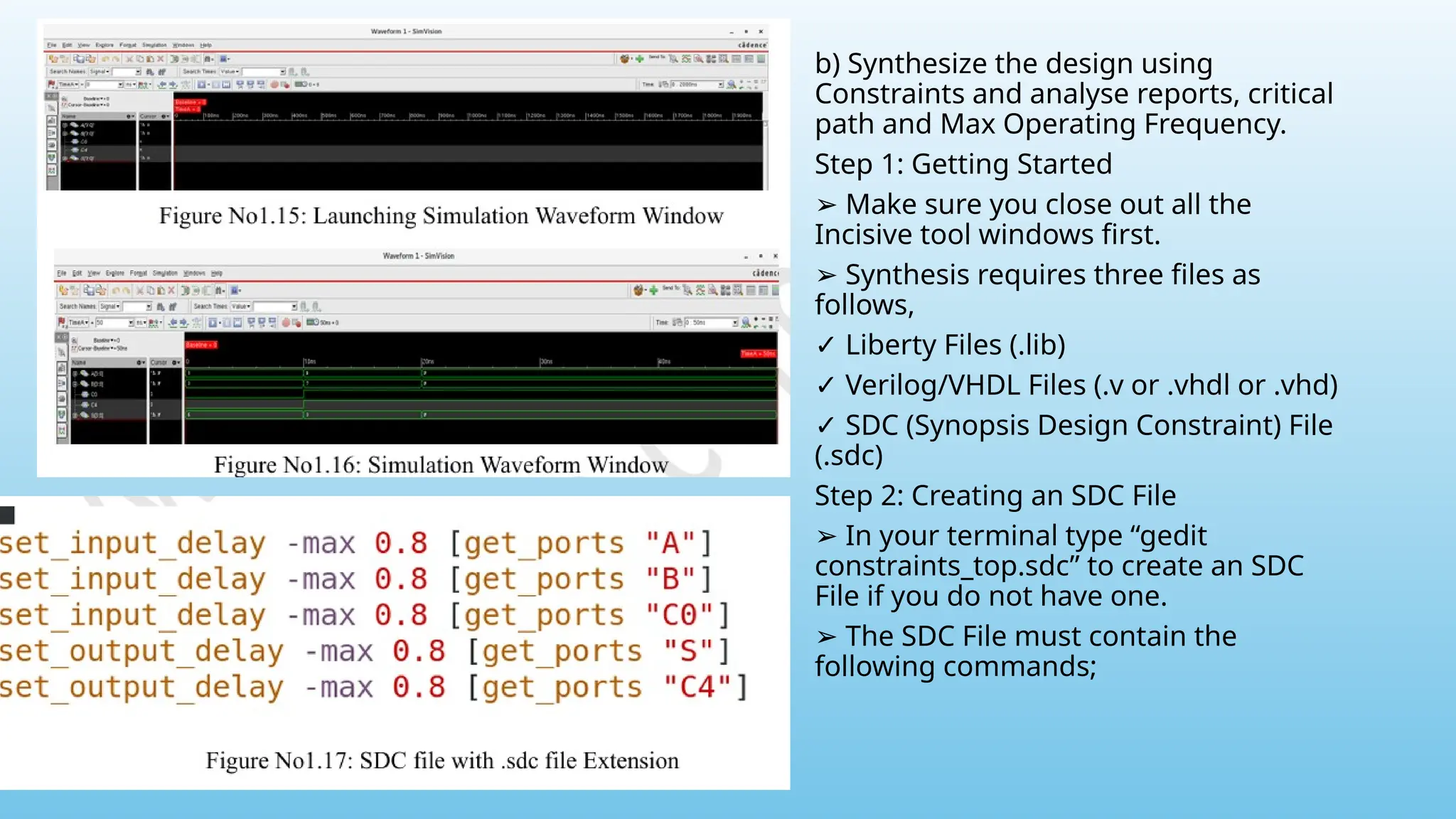
The document provides a comprehensive tutorial on designing and implementing a 4-bit adder circuit using full adders. It includes code examples for the 4-bit adder and test bench, as well as detailed steps for simulation, compilation, elaboration, and synthesis using specific tools and commands. Additionally, it outlines the creation and use of various files, such as .lib and .sdc files, necessary for the synthesis process.

![Code:
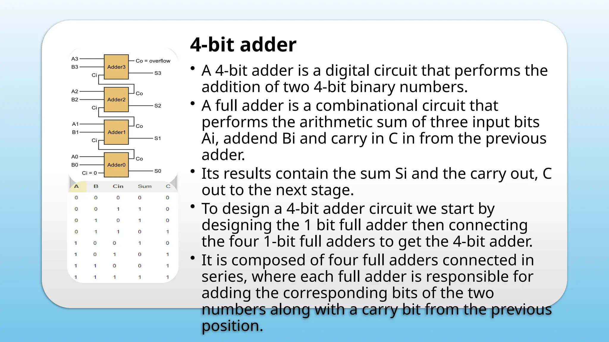
module four_bit_adder(A,B,C0,S,C4);
input [3:0] A,B;
input C0;
output [3:0] S;
output C4;
wire C1,C2,C3;
full_adder fa0(A[0],B[0],C0,S[0],C1);
full_adder fa1(A[1],B[1],C1,S[1],C2);
full_adder fa2(A[2],B[2],C2,S[2],C3);
full_adder fa3(A[3],B[3],C3,S[3],C4);
endmodule
module full_adder(A,B,Ci,S,Co);
input A,B,Ci;
output S,Co;
assign S=A^B^Ci;
assign Co=(A&B) | (Ci&(A^B));
endmodule](https://image.slidesharecdn.com/vlsipresentation-241027142449-b3f3c71e/75/Four-Bit-adder-4-bit-adder-Vlsi-Verilog-3-2048.jpg)
![Test bench code:
module test_4_bit;
reg[3:0] A;
reg[3:0] B;
reg C0;
wire[3:0] S;
wire C4;
four_bit_adder dut(A,B,C0,S,C4); initial begin
A=4’b0011; B=4’b0011; C0=1’b0;
#10; A=4’b1011; B=4’b0111; C0=1’b1;
#10; A=4’b1111; B=4’b1111; C0=1’b1;
#10;
end initial
#50 $finish;
endmodule](https://image.slidesharecdn.com/vlsipresentation-241027142449-b3f3c71e/75/Four-Bit-adder-4-bit-adder-Vlsi-Verilog-4-2048.jpg)
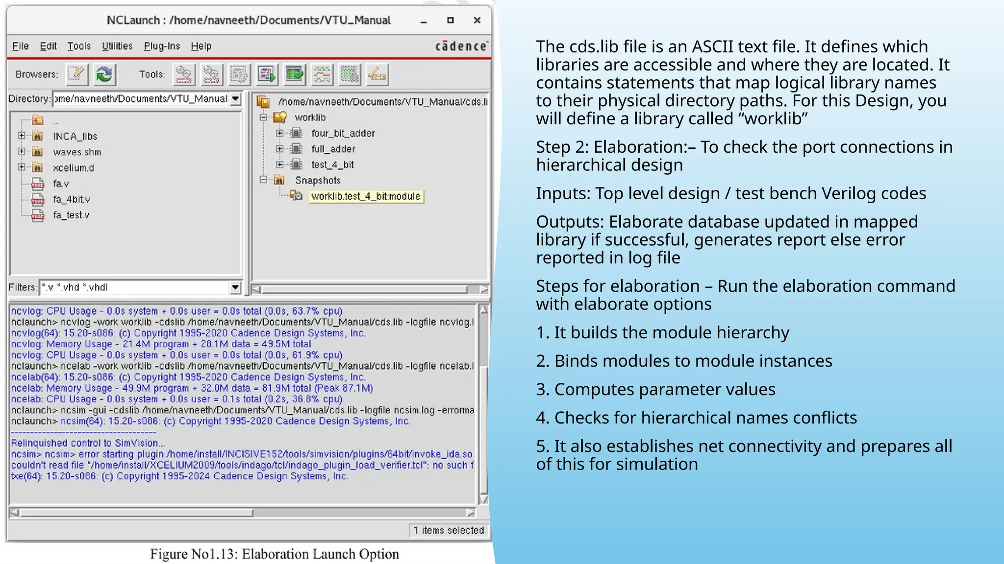
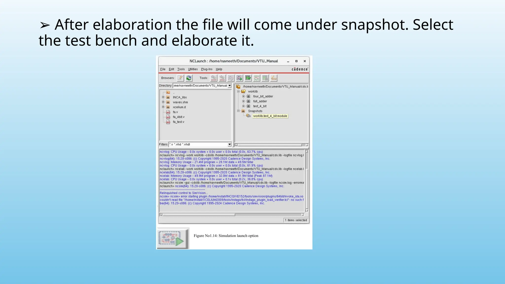
![Creating Source Codes
• In the Terminal, type gedit .v or .vhdl depending on the HDL Language you are to use (ex: 4bitadder.v).
• A Blank Document opens up into which the following source code can be typed down.
Note : File name should be with HDL Extension.
a) Verify the Functionality
➢ Three Codes shall be written for implementation of 4-bit Adder as follows,
✓ fa.v Single Bit 3-Input Full Adder [Sub-Module / Function]
→
✓ fa_4bit.v Top Module for Adding 4-bit Inputs.
→
✓ fa_test.v Test bench
→
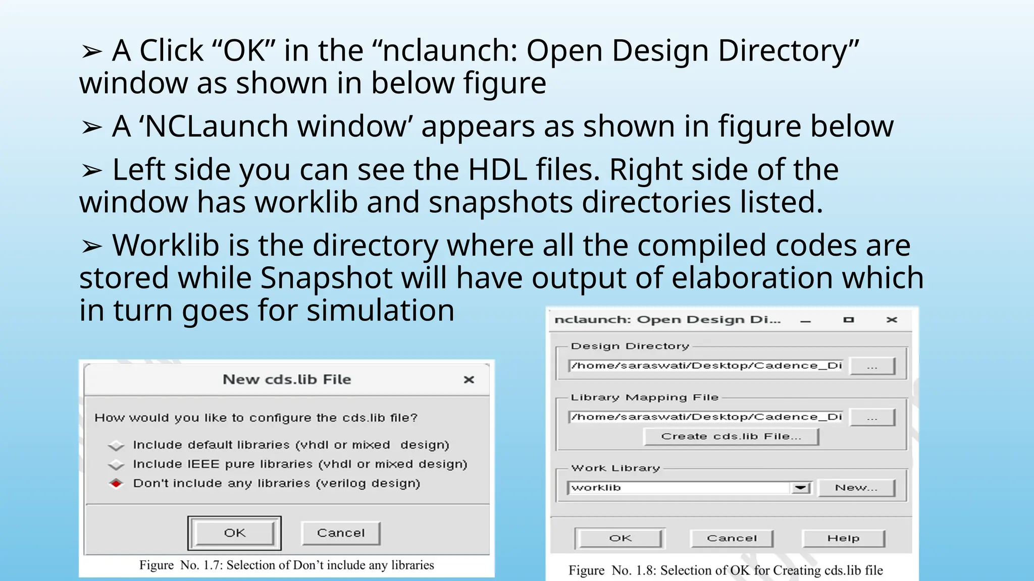
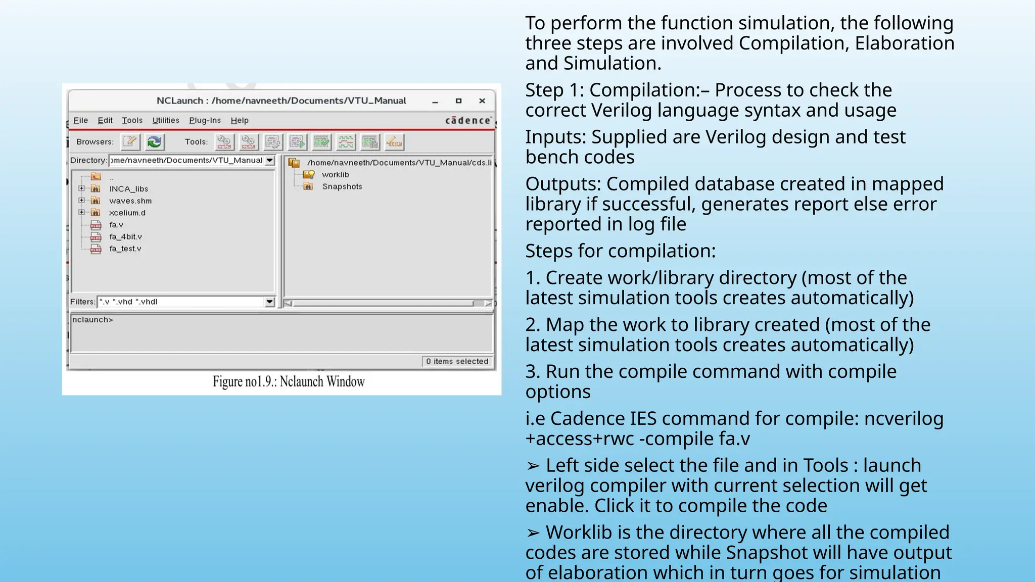
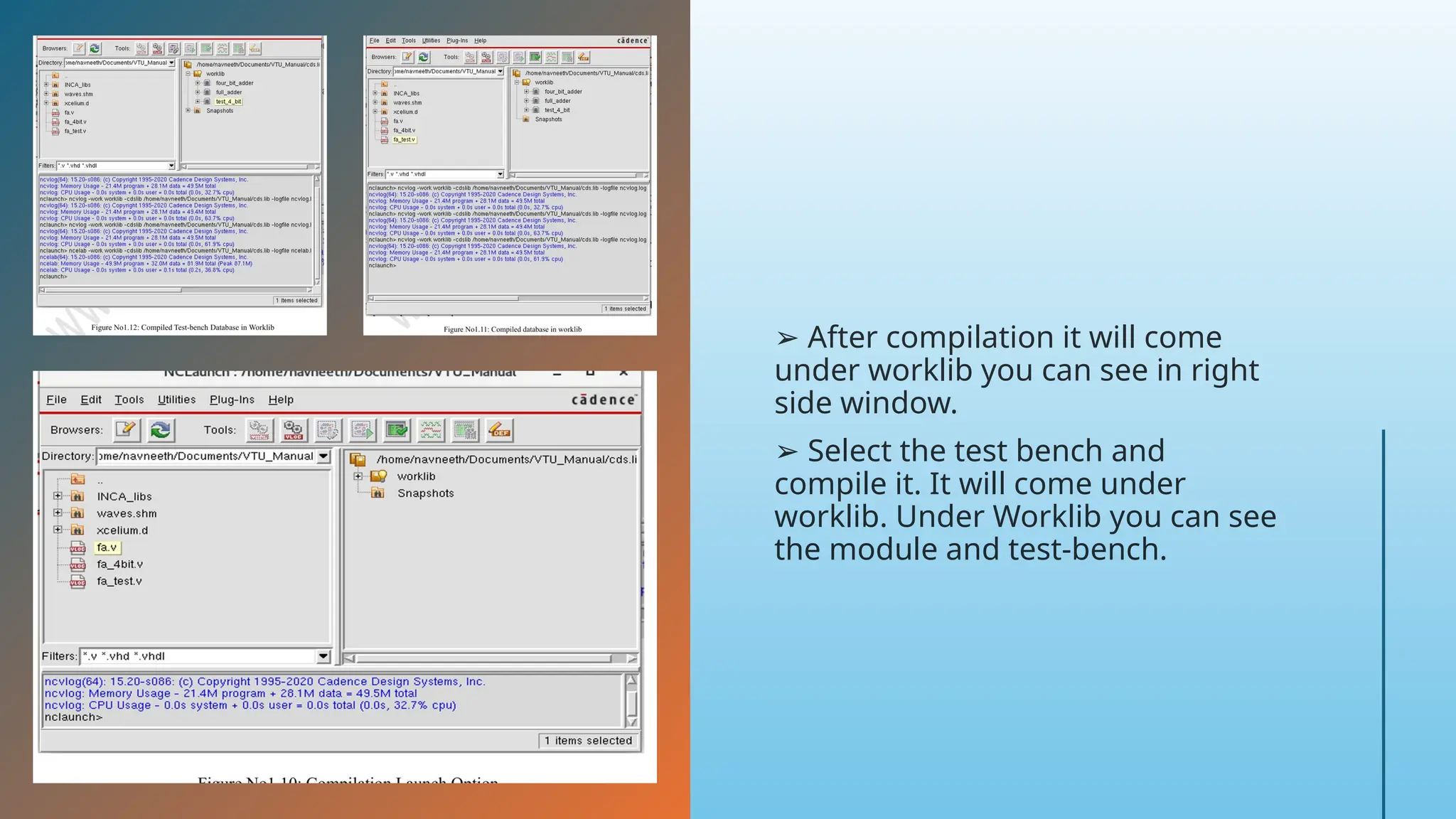
➢ To Launch Simulation tool
✓ linux:/> nclaunch -new& // “-new” option is used for invoking NCVERILOG
for the first time for any design
✓ linux:/> nclaunch& // On subsequent calls to NCVERILOG
➢ It will invoke the nclaunch window for functional simulation we can compile,elaborate and simulate it using
Multiple](https://image.slidesharecdn.com/vlsipresentation-241027142449-b3f3c71e/75/Four-Bit-adder-4-bit-adder-Vlsi-Verilog-5-2048.jpg)


![11. report_timing >
counter_timing.rep //Generates
Timing report for worst
datapath and dumps into file
12. report_area >
counter_area.rep //Generates
Synthesis Area report and
dumps into a file
13. report_power >
counter_power.rep //Generates
Power Report [Pre-Layout]
14. write_hdl > counter_netlist.v
//Creates readable Netlist File
15. write_sdc > counter_sdc.sdc
//Creates Block Level SDC](https://image.slidesharecdn.com/vlsipresentation-241027142449-b3f3c71e/75/Four-Bit-adder-4-bit-adder-Vlsi-Verilog-15-2048.jpg)


![Code:
module four_bit_adder(A,B,C0,S,C4);
input [3:0] A,B;
input C0;
output [3:0] S;
output C4;
wire C1,C2,C3;
full_adder fa0(A[0],B[0],C0,S[0],C1);
full_adder fa1(A[1],B[1],C1,S[1],C2);
full_adder fa2(A[2],B[2],C2,S[2],C3);
full_adder fa3(A[3],B[3],C3,S[3],C4);
endmodule
module full_adder(A,B,Ci,S,Co);
input A,B,Ci;
output S,Co;
assign S=A^B^Ci;
assign Co=(A&B) | (Ci&(A^B));
endmodule](https://crownmelresort.com/image.slidesharecdn.com/vlsipresentation-241027142449-b3f3c71e/75/Four-Bit-adder-4-bit-adder-Vlsi-Verilog-3-2048.jpg)
![Test bench code:
module test_4_bit;
reg[3:0] A;
reg[3:0] B;
reg C0;
wire[3:0] S;
wire C4;
four_bit_adder dut(A,B,C0,S,C4); initial begin
A=4’b0011; B=4’b0011; C0=1’b0;
#10; A=4’b1011; B=4’b0111; C0=1’b1;
#10; A=4’b1111; B=4’b1111; C0=1’b1;
#10;
end initial
#50 $finish;
endmodule](https://crownmelresort.com/image.slidesharecdn.com/vlsipresentation-241027142449-b3f3c71e/75/Four-Bit-adder-4-bit-adder-Vlsi-Verilog-4-2048.jpg)
![Creating Source Codes
• In the Terminal, type gedit .v or .vhdl depending on the HDL Language you are to use (ex: 4bitadder.v).
• A Blank Document opens up into which the following source code can be typed down.
Note : File name should be with HDL Extension.
a) Verify the Functionality
➢ Three Codes shall be written for implementation of 4-bit Adder as follows,
✓ fa.v Single Bit 3-Input Full Adder [Sub-Module / Function]
→
✓ fa_4bit.v Top Module for Adding 4-bit Inputs.
→
✓ fa_test.v Test bench
→
➢ To Launch Simulation tool
✓ linux:/> nclaunch -new& // “-new” option is used for invoking NCVERILOG
for the first time for any design
✓ linux:/> nclaunch& // On subsequent calls to NCVERILOG
➢ It will invoke the nclaunch window for functional simulation we can compile,elaborate and simulate it using
Multiple](https://crownmelresort.com/image.slidesharecdn.com/vlsipresentation-241027142449-b3f3c71e/75/Four-Bit-adder-4-bit-adder-Vlsi-Verilog-5-2048.jpg)


![11. report_timing >
counter_timing.rep //Generates
Timing report for worst
datapath and dumps into file
12. report_area >
counter_area.rep //Generates
Synthesis Area report and
dumps into a file
13. report_power >
counter_power.rep //Generates
Power Report [Pre-Layout]
14. write_hdl > counter_netlist.v
//Creates readable Netlist File
15. write_sdc > counter_sdc.sdc
//Creates Block Level SDC](https://crownmelresort.com/image.slidesharecdn.com/vlsipresentation-241027142449-b3f3c71e/75/Four-Bit-adder-4-bit-adder-Vlsi-Verilog-15-2048.jpg)