Downloaded 12 times
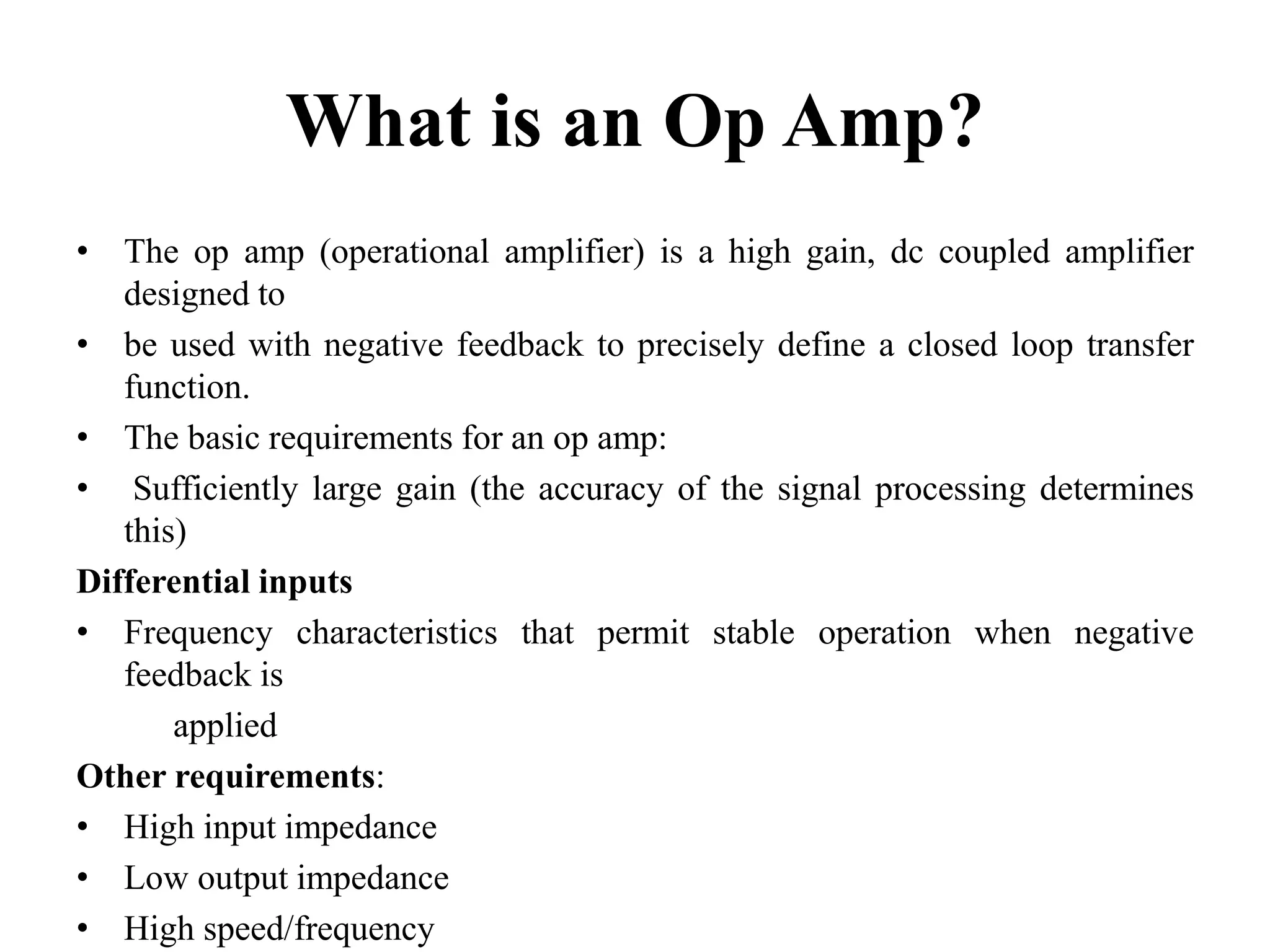
![Linear Op-amp Operation: Non-Inverting Use
• An op-amp can use negative feedback to set the
closed-loop gain as a function of the circuit external
elements (resistors), independent of the op-amp gain,
as long as the internal op-amp gain is very high
• Shown at left is an ideal op-amp in a non-inverting
configuration with negative feedback provided by
voltage divider R1, R2
• Determination of closed-loop gain:
– Since the input current is assumed zero, we can
write v- = R1/(R1 + R2)vOUT
– But, since v+ =~ v- for the opamp operation in its
linear region, we can write
v- = vIN = R1/(R1 + R2)vOUT
or, vOUT = ((R1 + R2)/R1)vIN
• We can derive the same expression by writing
vOUT = A(v+- v-) = A{vIN – [R1/(R1 + R2)] vOUT}
and solving for vOUT with A>>1
Look at Example 2.1 and plot transfer curve.](https://image.slidesharecdn.com/analogcmosdesign-191009075649/75/Analog-CMOS-design-6-2048.jpg)
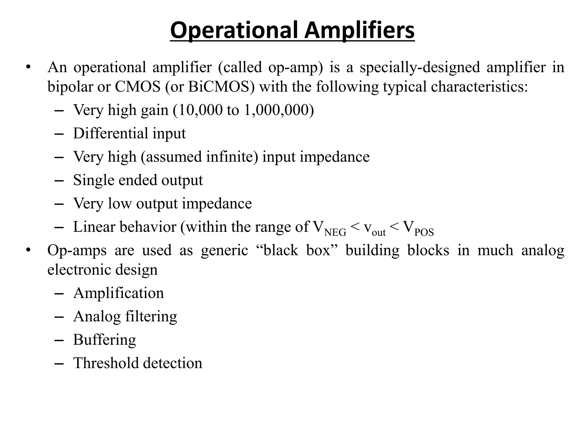
![Input Resistance for Inverting and Non-inverting Op-amps
• The non-inverting op-amp configuration of slide 2-4 has an apparent input
resistance of infinity, since iIN = 0 and RIN = vIN/iIN = vIN/0 = infinity
• The inverting op-amp configuration, however, has an apparent input resistance
of R1
– since RIN = vIN/iIN = vIN/[(vIN – 0)/R1] = R1](https://image.slidesharecdn.com/analogcmosdesign-191009075649/75/Analog-CMOS-design-9-2048.jpg)


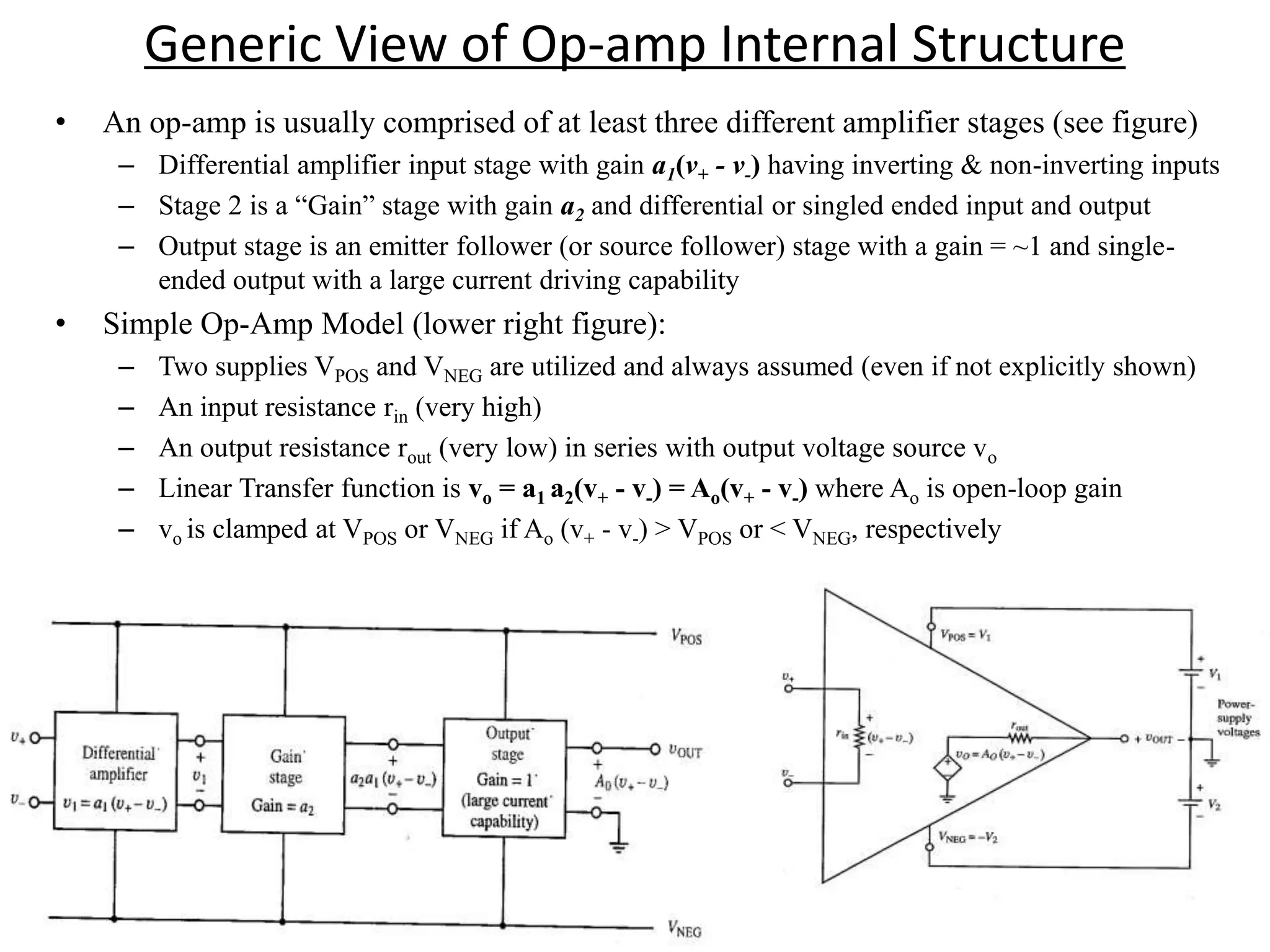
![Linear Op-amp Operation: Non-Inverting Use
• An op-amp can use negative feedback to set the
closed-loop gain as a function of the circuit external
elements (resistors), independent of the op-amp gain,
as long as the internal op-amp gain is very high
• Shown at left is an ideal op-amp in a non-inverting
configuration with negative feedback provided by
voltage divider R1, R2
• Determination of closed-loop gain:
– Since the input current is assumed zero, we can
write v- = R1/(R1 + R2)vOUT
– But, since v+ =~ v- for the opamp operation in its
linear region, we can write
v- = vIN = R1/(R1 + R2)vOUT
or, vOUT = ((R1 + R2)/R1)vIN
• We can derive the same expression by writing
vOUT = A(v+- v-) = A{vIN – [R1/(R1 + R2)] vOUT}
and solving for vOUT with A>>1
Look at Example 2.1 and plot transfer curve.](https://crownmelresort.com/image.slidesharecdn.com/analogcmosdesign-191009075649/75/Analog-CMOS-design-6-2048.jpg)


![Input Resistance for Inverting and Non-inverting Op-amps
• The non-inverting op-amp configuration of slide 2-4 has an apparent input
resistance of infinity, since iIN = 0 and RIN = vIN/iIN = vIN/0 = infinity
• The inverting op-amp configuration, however, has an apparent input resistance
of R1
– since RIN = vIN/iIN = vIN/[(vIN – 0)/R1] = R1](https://crownmelresort.com/image.slidesharecdn.com/analogcmosdesign-191009075649/75/Analog-CMOS-design-9-2048.jpg)


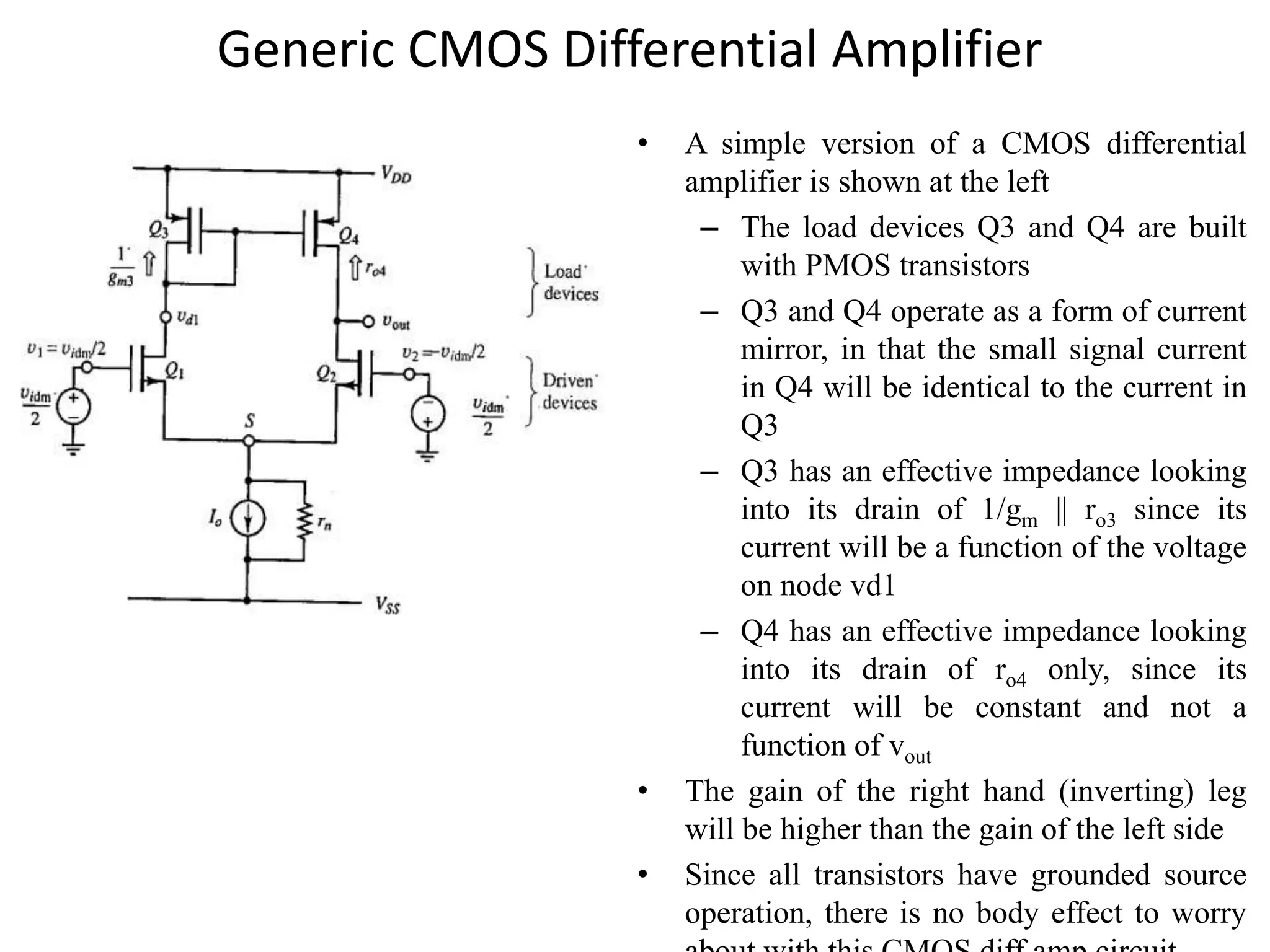
The document discusses operational amplifiers (op-amps) and differential amplifiers. It provides details on the basic requirements and characteristics of op-amps such as high gain, differential inputs, and high input/low output impedance. It describes the typical internal structure of an op-amp including differential, gain, and output stages. Ideal op-amp assumptions and linear op-amp operation in inverting and non-inverting configurations are also covered. The document then discusses differential amplifiers, including their advantages and applications in analog circuits. It provides details on a proposed CMOS differential amplifier design and its high common-mode rejection ratio.
The presentation introduces Analog CMOS Design, emphasizing operational amplifiers.
Op-amps are high-gain amplifiers with various characteristics like high input impedance and low output impedance for precise signal processing.
Description of non-inverting and inverting configurations using negative feedback for closed-loop gain adjustment.
Differentiation in input resistance between non-inverting (infinite) and inverting (equal to R1) configurations.
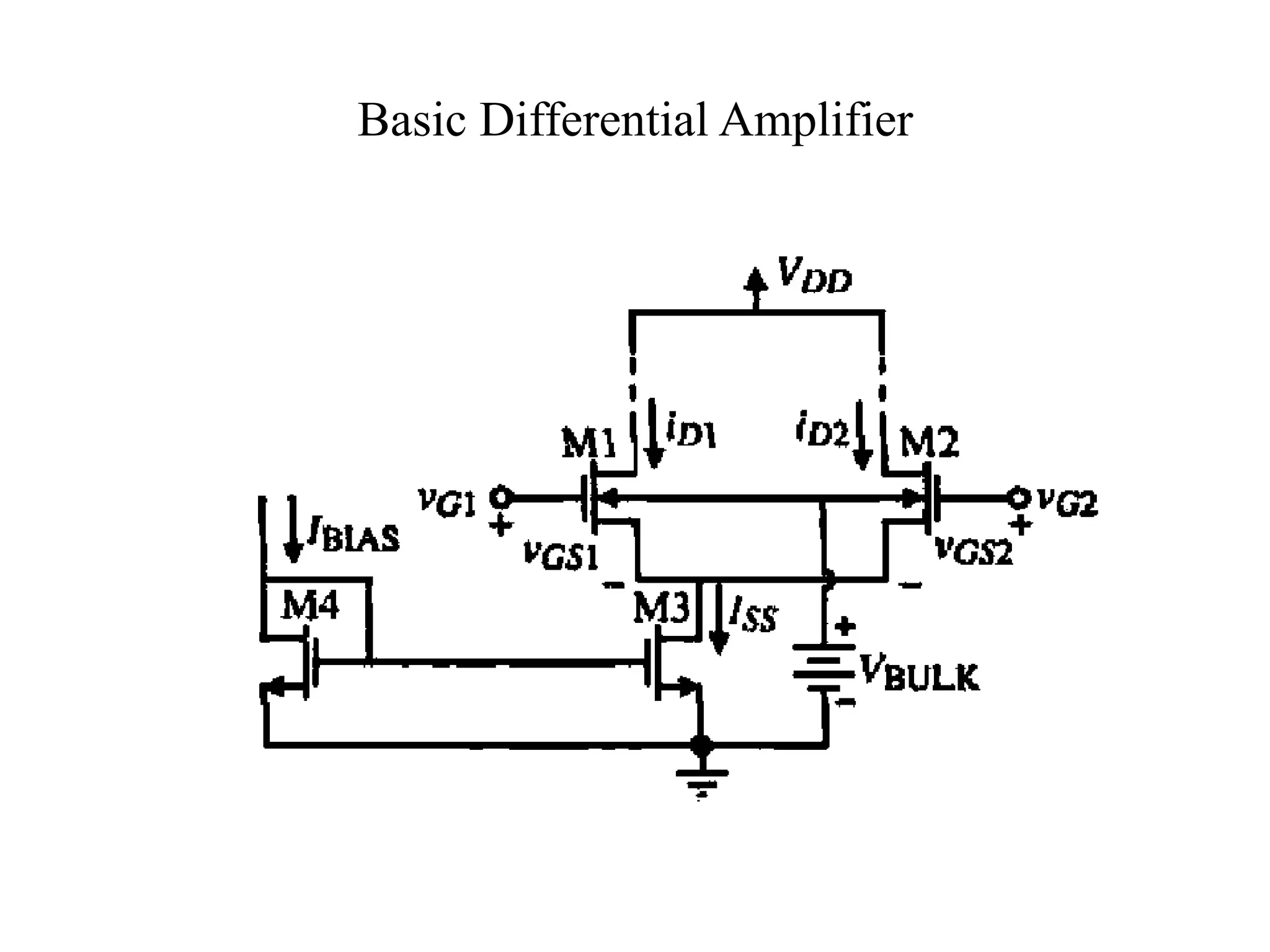
Differential amplifiers used in analog electronics highlighting their advantages, including large input resistance and high gain.
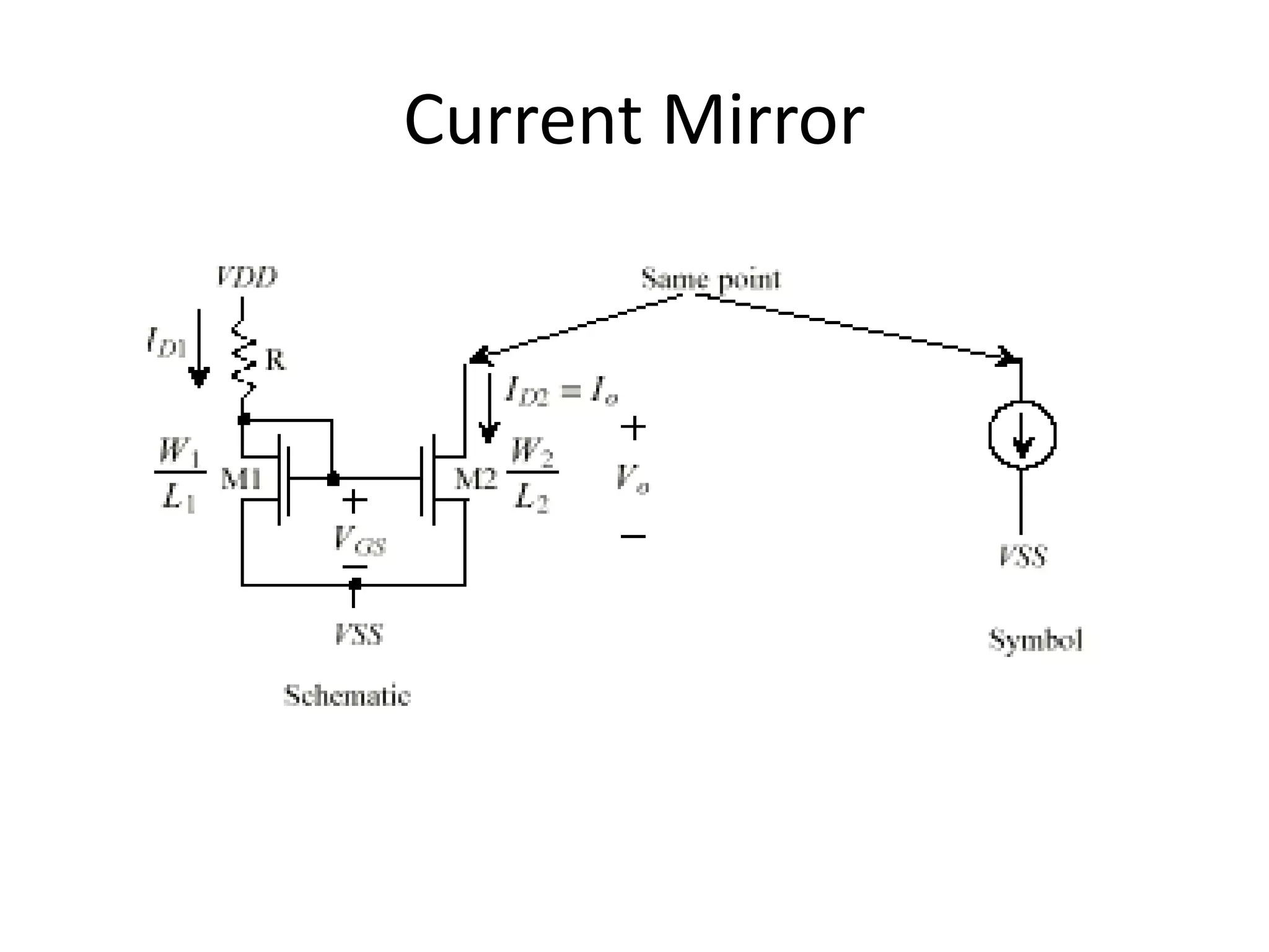
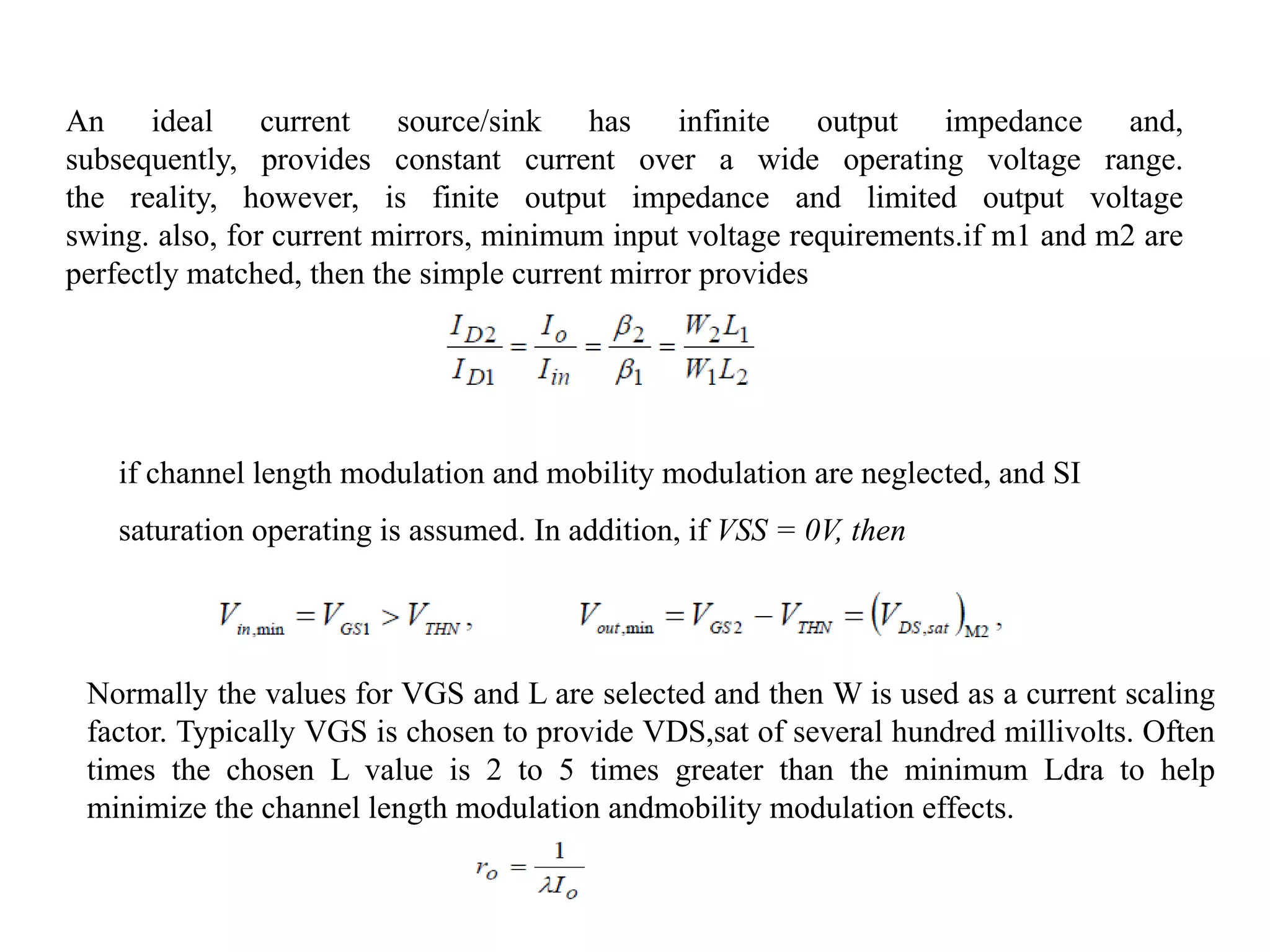
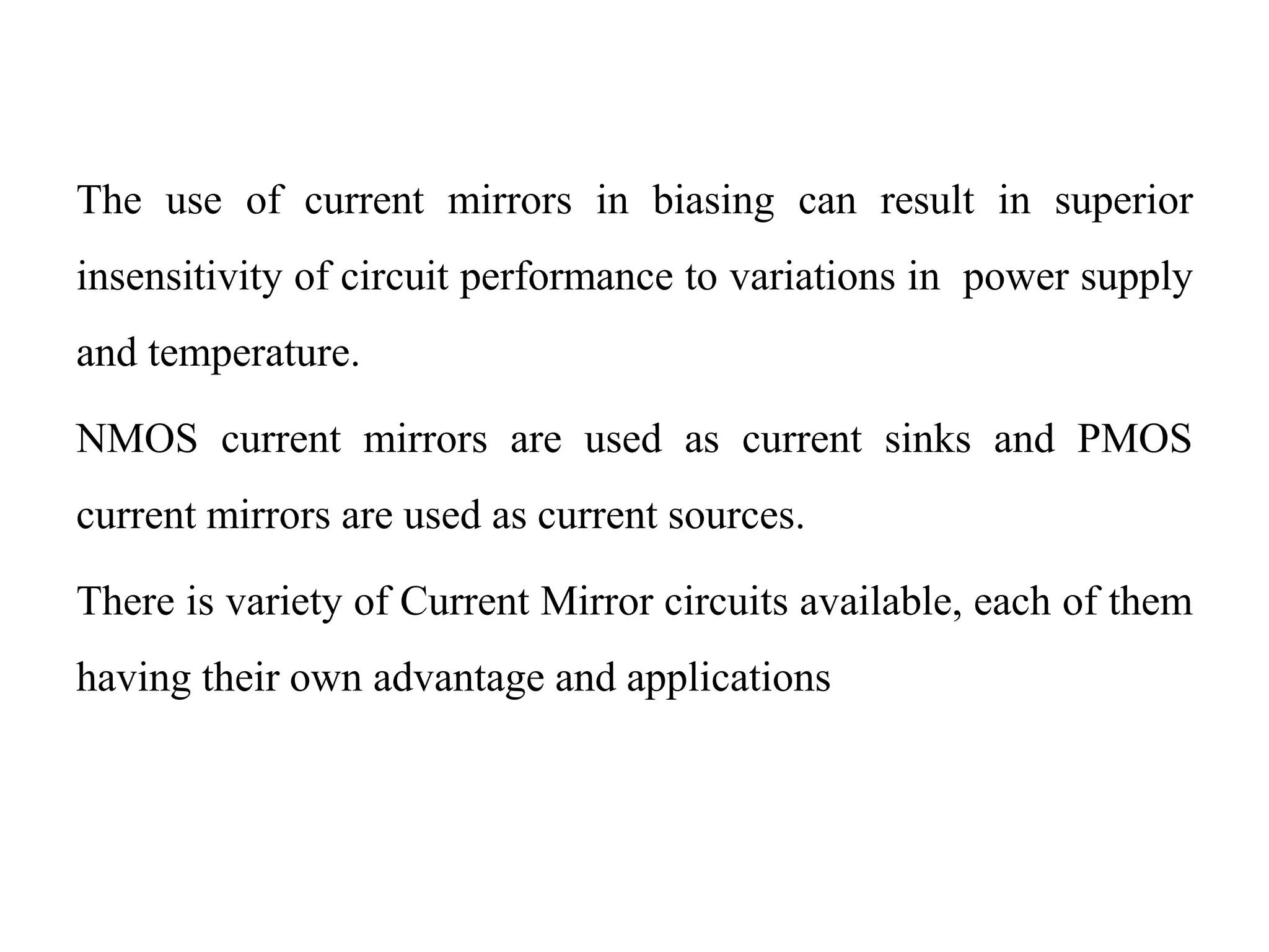
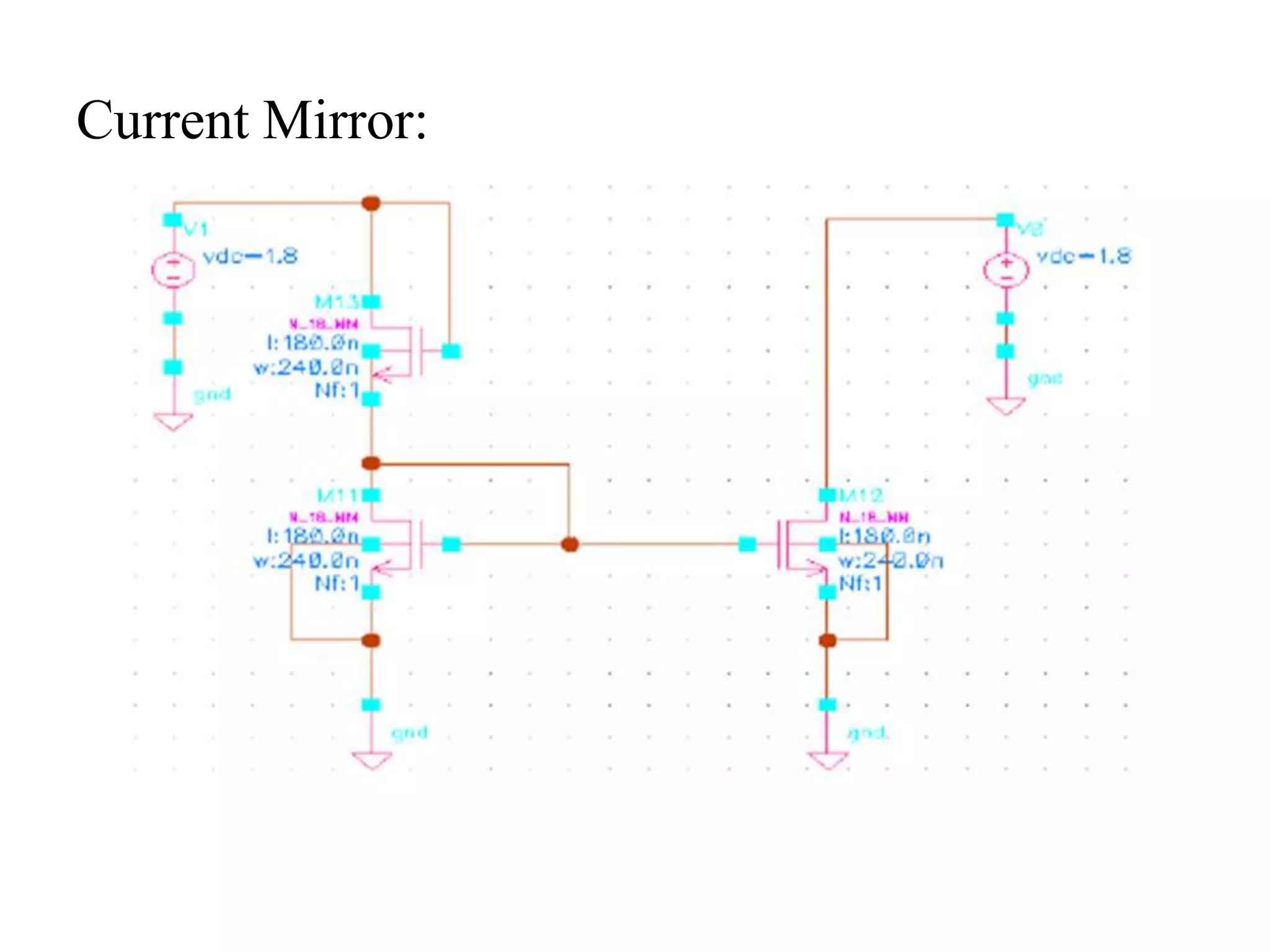
Introduction to current mirrors using MOS transistors for biasing and load devices, explaining how they relate to circuit performance.
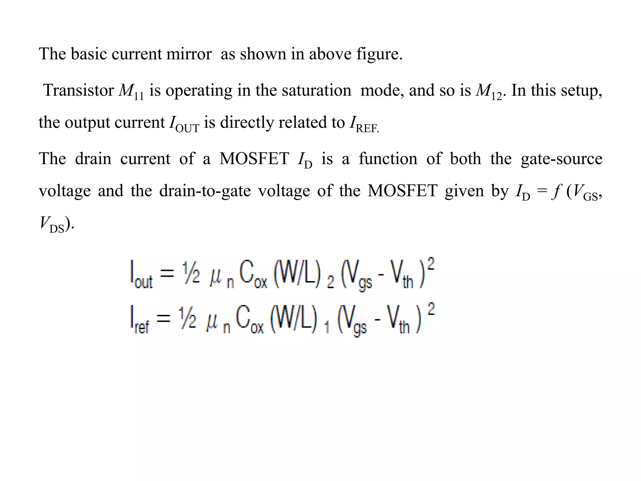
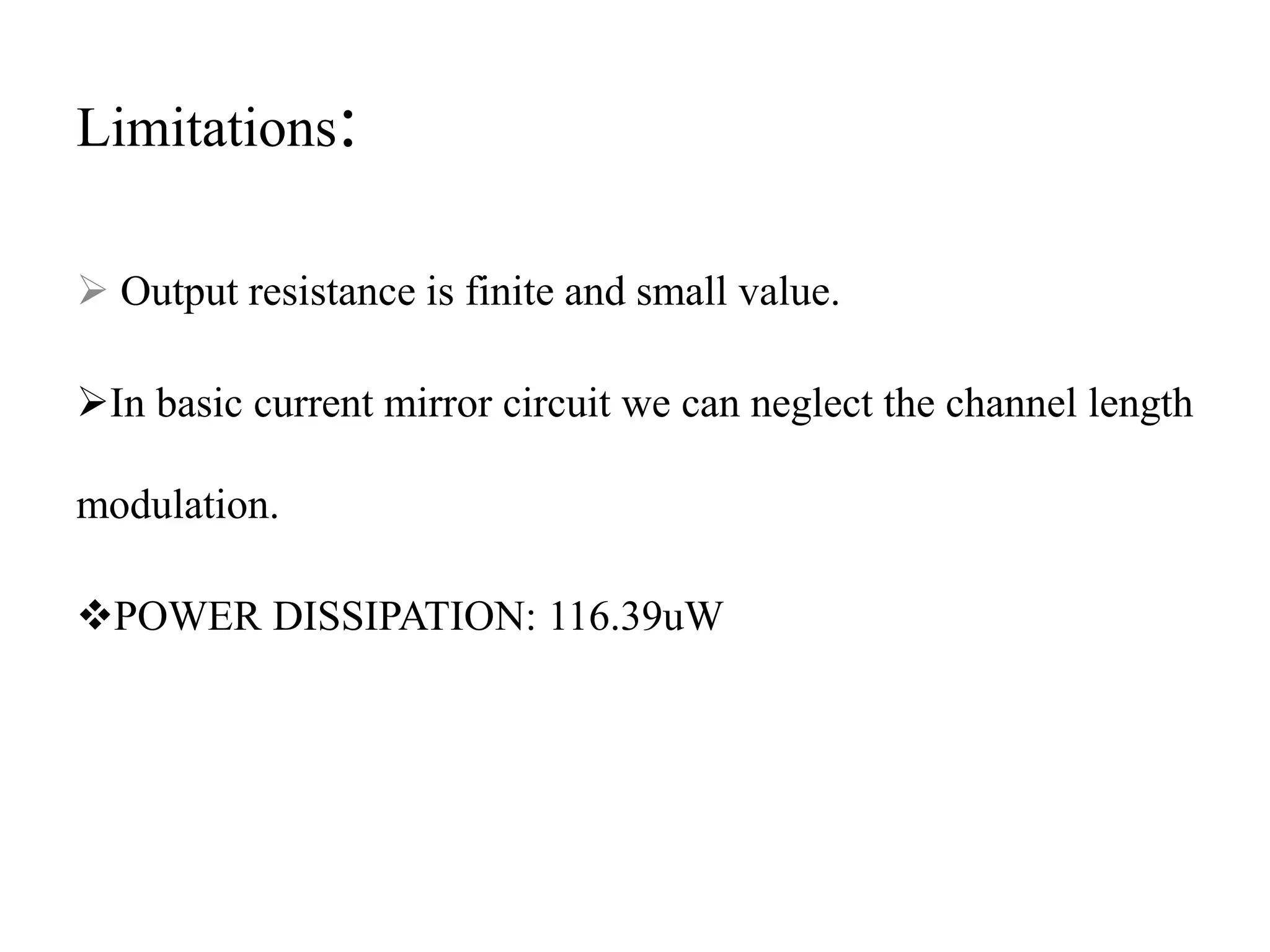
Basic current mirror functionality, including output current relations and limitations in terms of output resistance and power dissipation.
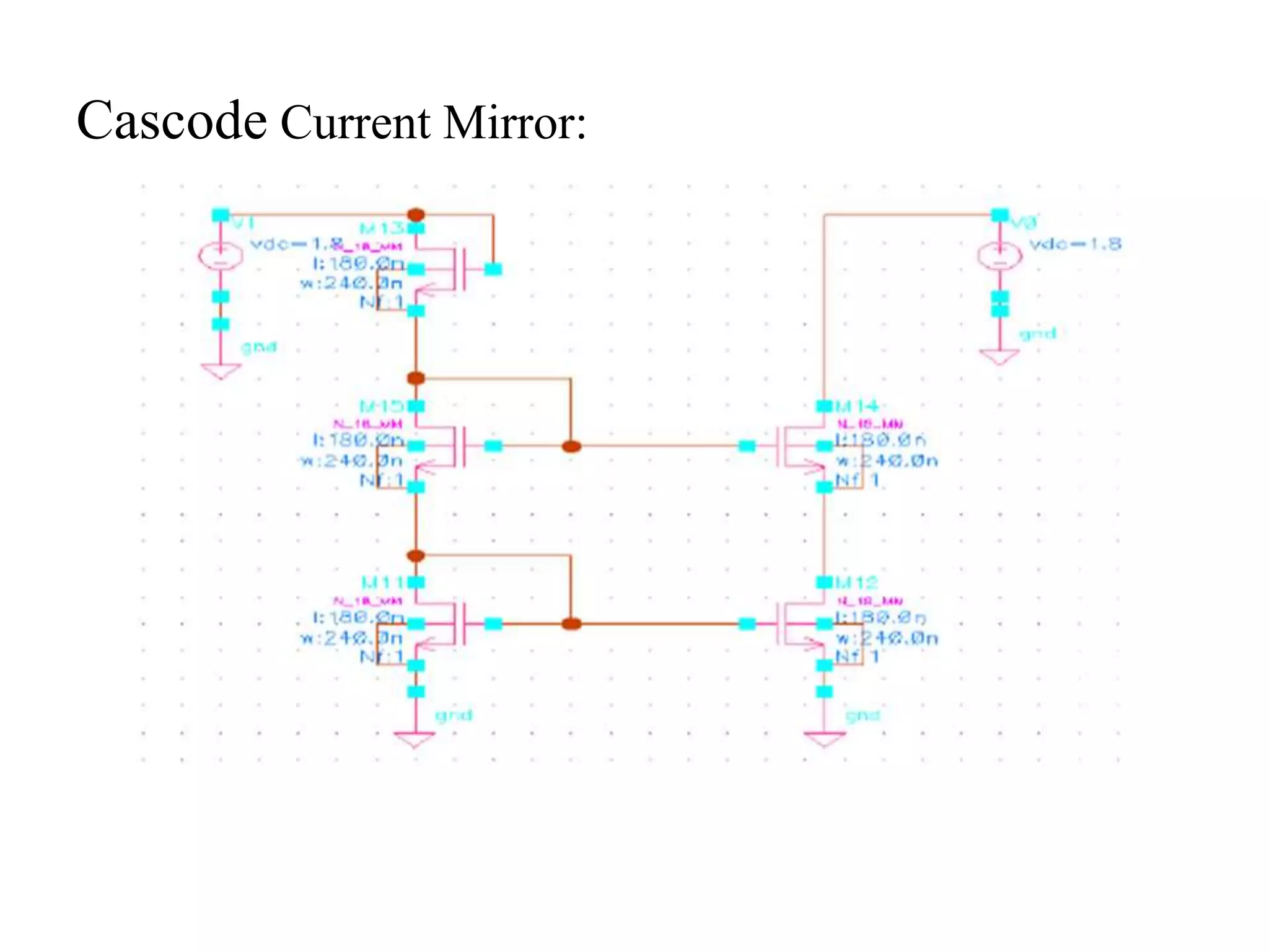
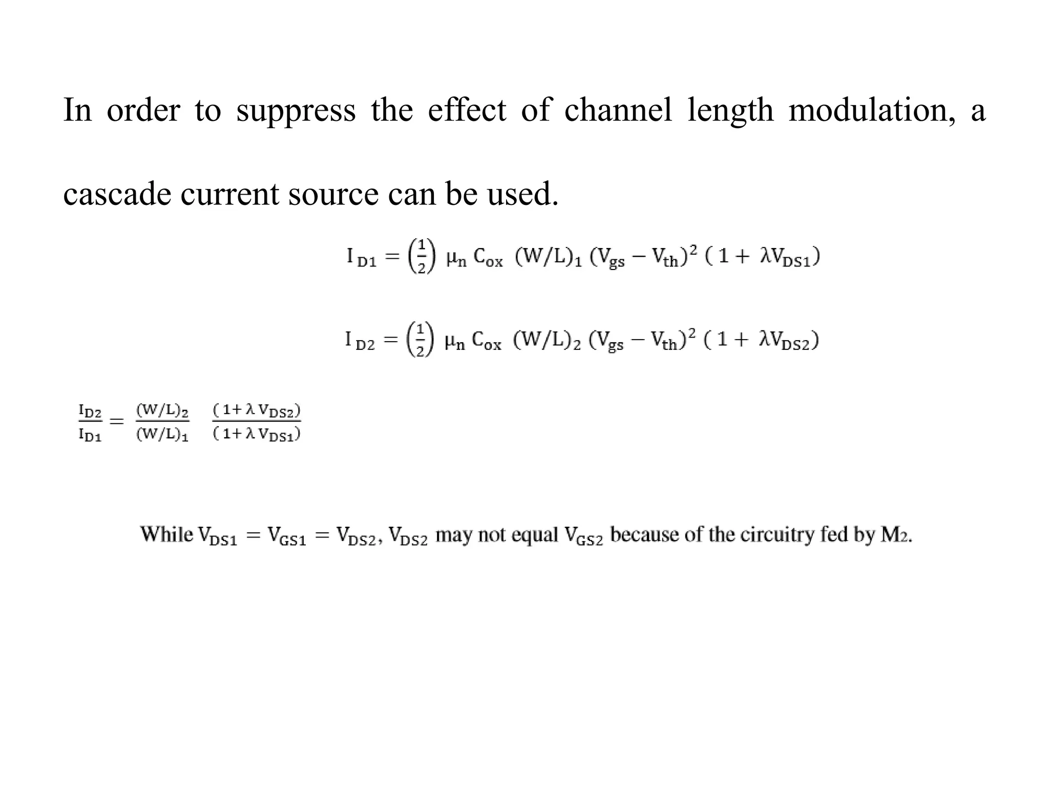
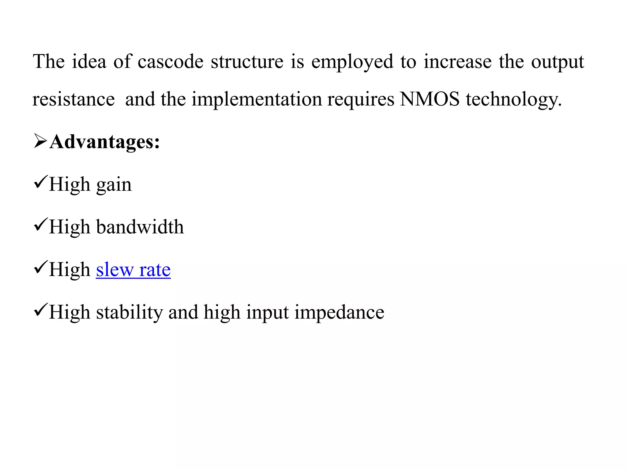
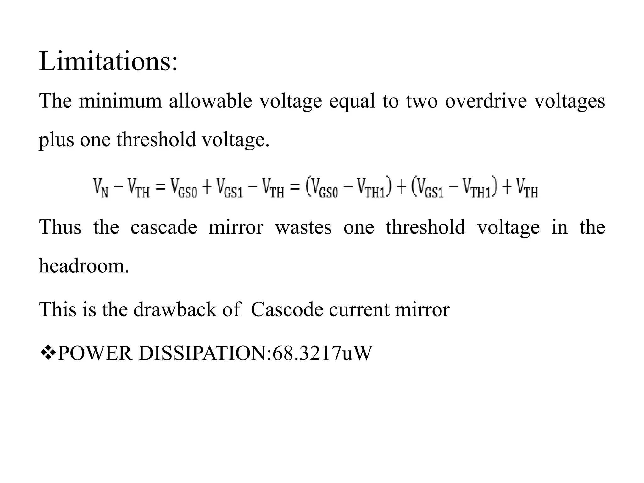
Using cascode current mirrors for higher output resistance, detailing advantages like high gain, bandwidth, and some limitations.
Identifies applications of current mirrors in high-speed data converters and oscillators.
Comparison of CMOS Voltage Divider based Current Mirror with basic and cascode types, focusing on power efficiency.
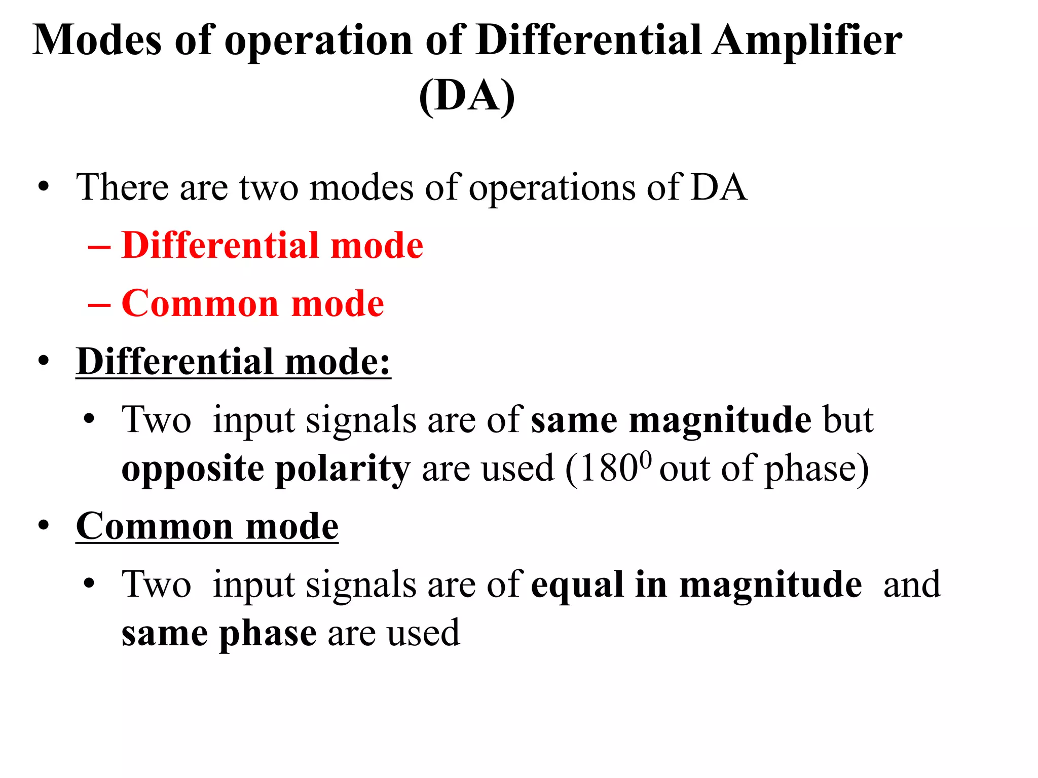
Differential vs common mode operations in amplifiers and their compatibility with integrated circuits.
Behavior of differential amplifiers designed to amplify differences between signals while suppressing noise.
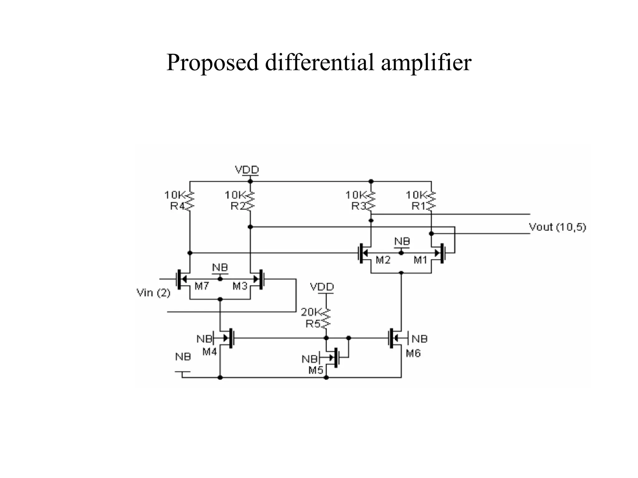
Presentation of a proposed differential amplifier with high common mode rejection ratio focusing on specific transistor configurations.


![RF Module Design - [Chapter 6] Power Amplifier](https://cdn.slidesharecdn.com/ss_thumbnails/rfch6-150613070347-lva1-app6891-thumbnail.jpg?width=640&height=640&fit=bounds)