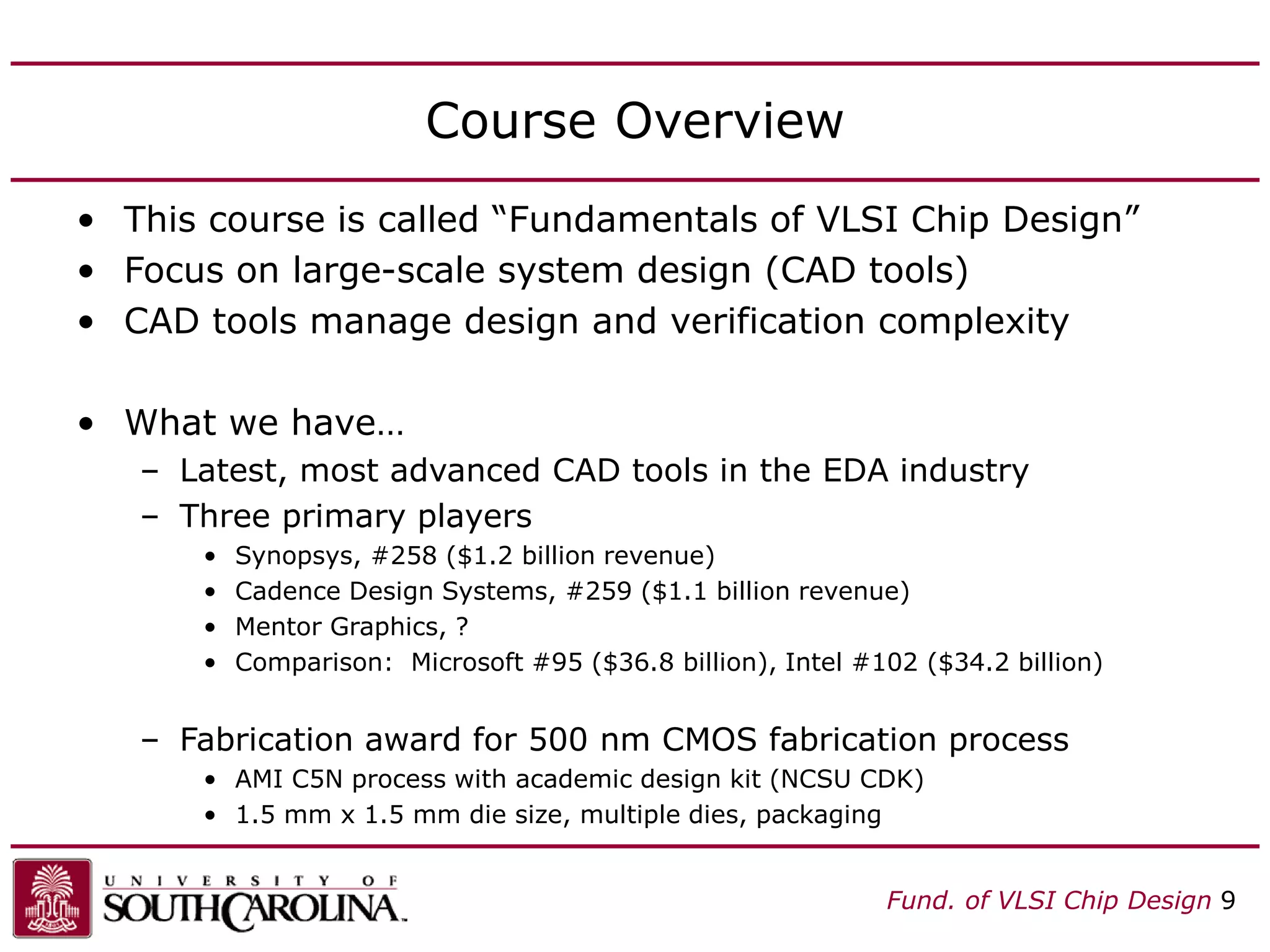
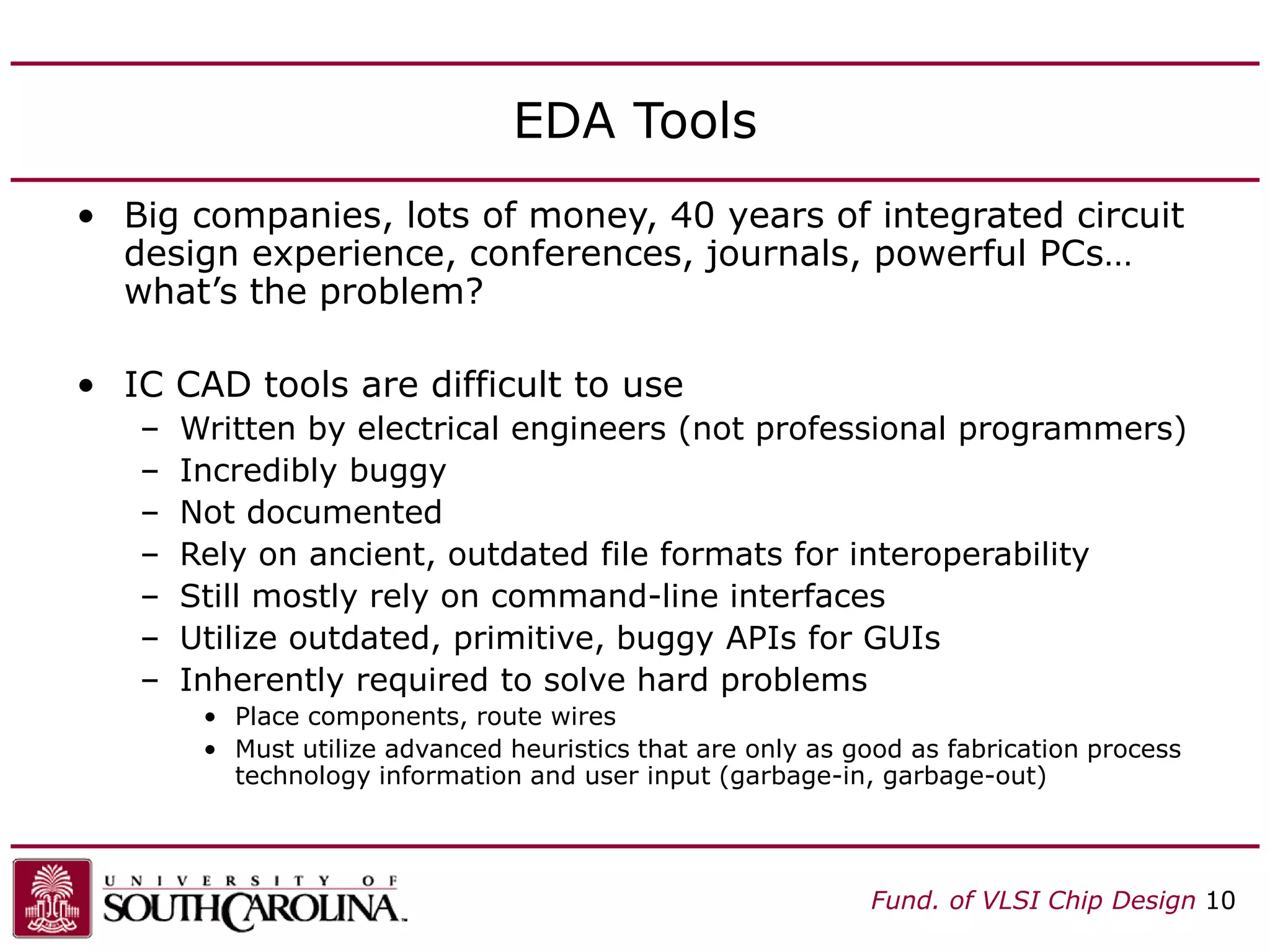
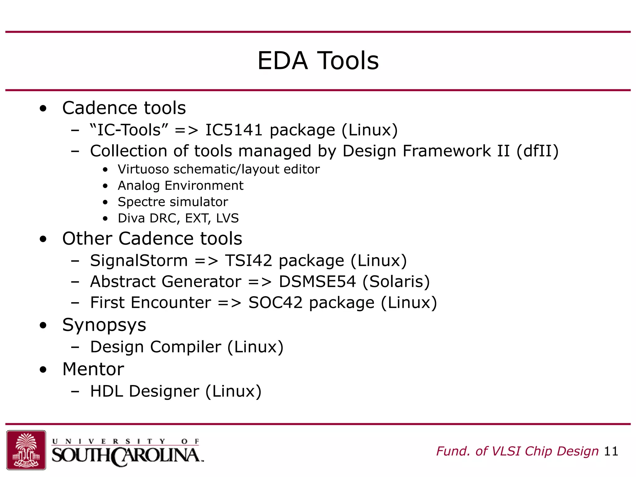
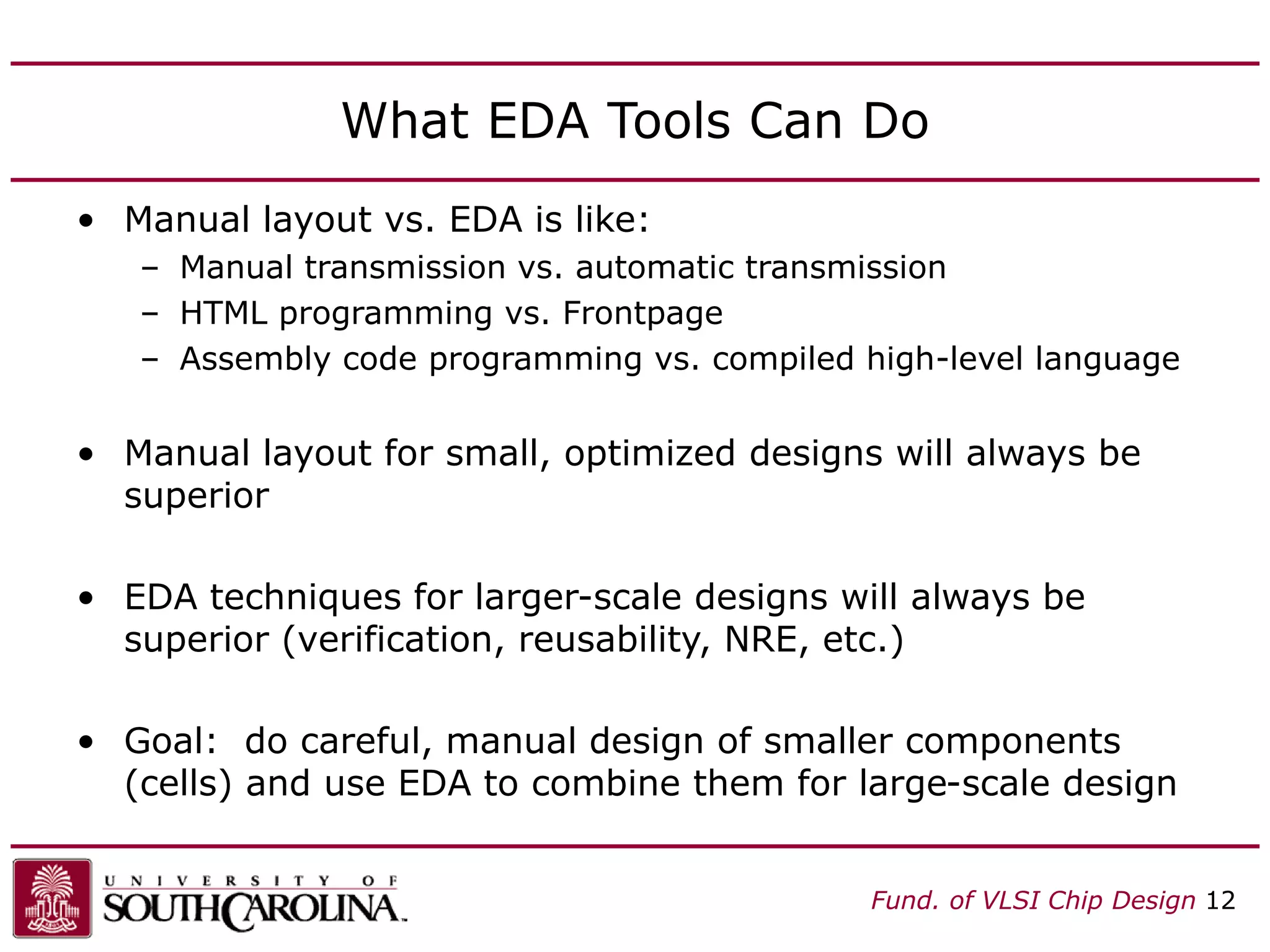
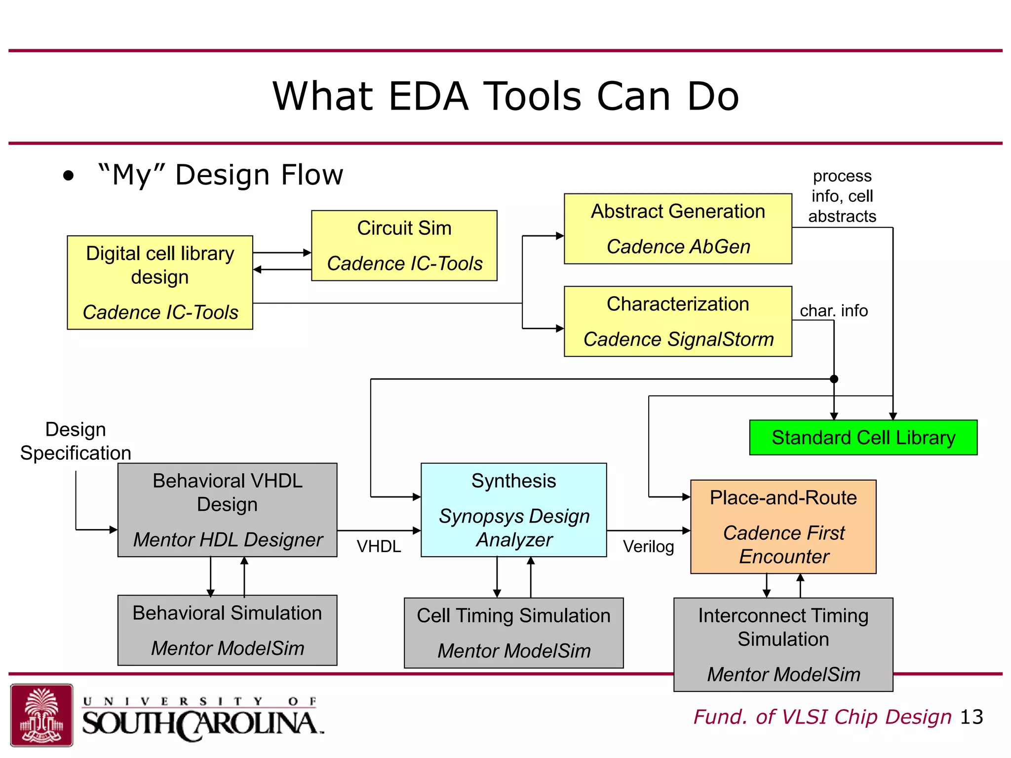
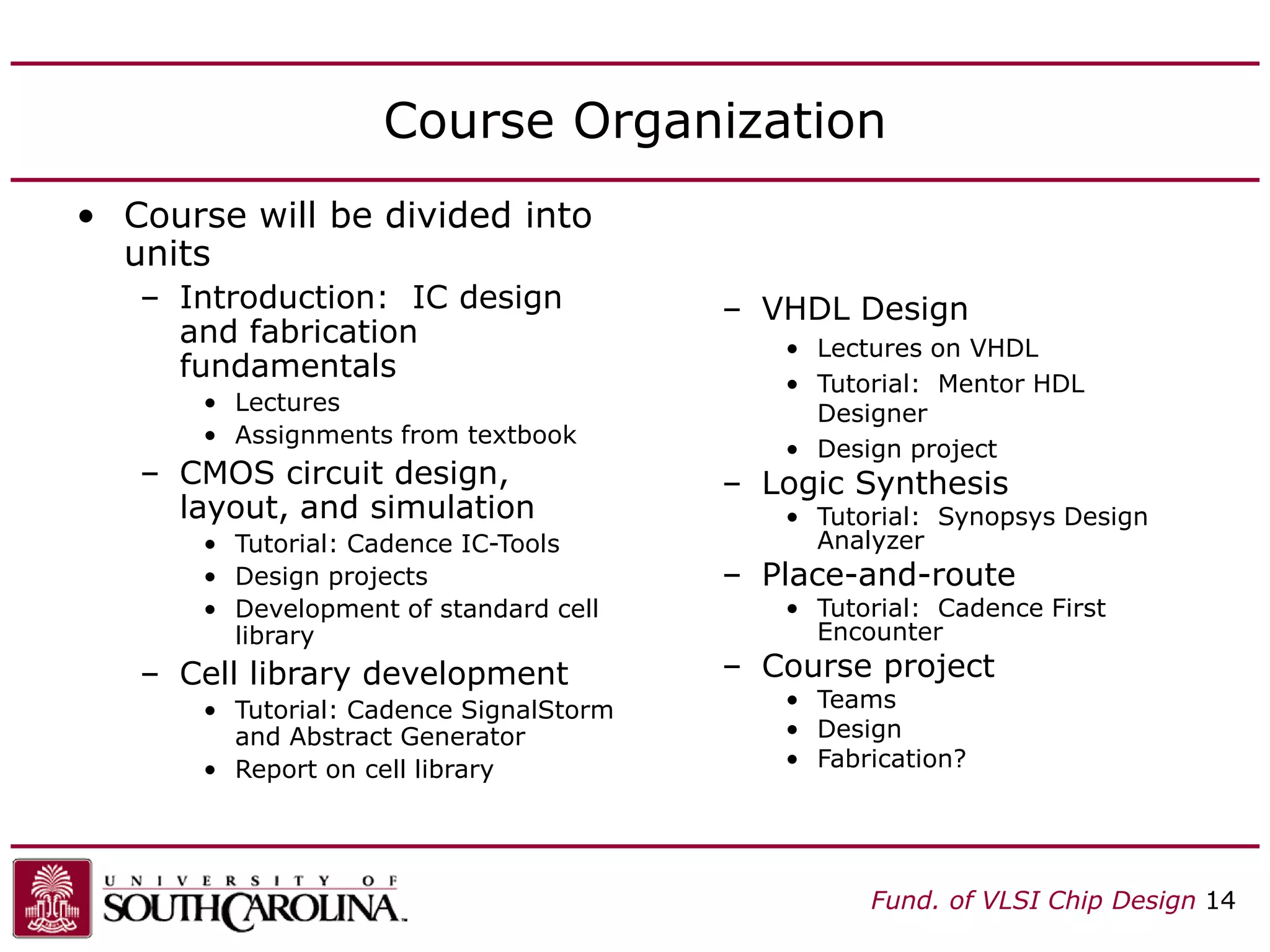
CSCE 613: Fundamentals of VLSI Chip Design
Instructor: Jason D. Bakos
Fund. of VLSI Chip Design 2
VLSI Design
• What is VLSI?
– “Very Large Scale Integration”
– Defines integration level
– 1980s hold-over from outdated taxonomy for integration levels
• Obviously influenced from frequency bands, i.e. HF, VHF, UHF
– Sources disagree on what is measured (gates or transistors?)
• SSI – Small-Scale Integration (0-102)
• MSI – Medium-Scale Integration (102-103)
• LSI – Large-Scale Integration (103-105)
• VLSI – Very Large-Scale Integration (105-107)
• ULSI – Ultra Large-Scale Integration (>=107)
Fund. of VLSI Chip Design 3
Integration Level Trends
Obligatory historical Moore’s law plot
Fund. of VLSI Chip Design 4
Integrated Circuits/MEMs
• Today, VLSI refers to systems impl. w/integrated circuits
– Integrated circuit refers mostly to general manufacturing
technique
• micro/nano-scale devices on a semiconductor (crystalline) substrate
• Formed using chemical/lithography processing
• What kind of devices / structures?
– transistors (bipolar, MOSFET)
– wires (interconnects and passive devices)
– diodes (junction, LEDs, VCSELs, MSM, photoconductor, PiN)
– MEMs (integration of piezoelectrics and mechanics based on
static electrical fields: accelerometers, gyroscopes, pressure
sensors, micro-mirrors)
• For CMOS digital design, we only use MOSFET transistors
(used as switches) and wires
Fund. of VLSI Chip Design 5
Chips
• Integrated circuits consist of:
– A small square or rectangular “die”, < 1mm thick
• Small die: 1.5 mm x 1.5 mm => 2.25 mm2
• Large die: 15 mm x 15 mm => 225 mm2
– Larger die sizes mean:
• More logic, memory
• Less volume
• Less yield
– Dies are made from silicon (substrate)
• Substrate provides mechanical support and electrical common
point
Fund. of VLSI Chip Design 6
VLSI Design
• Draw polygons that represent layers deposited-on or
infused-into the substrate
– More of an art than science
• One 2-input NAND gate with 4 transistors
• Typical microprocessor contains 50 – 200 million transistors
(10-50 million gates)
Scale:
approximately
10 um x 10 um
Fund. of VLSI Chip Design 7
VLSI Design
• Manual layout design is obviously not practical
• Design complexity:
– Manually drawing layout for a billion transistors would take too long
– Even if we could…
• How to verify (test) designs for functionality, speed, power, etc.?
– Complexity scales faster than actual design
• How to reuse designs?
• How to create human-readable designs?
• How to speed-up design process?
• These problems form a great deal of work
– Electronic Design Automation (EDA)
– a.k.a. CAD
• Advancing EDA technology, fabrication technology, designs and
microarchitectures, and IP form bulk of work (and money) in the
industry
Fund. of VLSI Chip Design 8
EDA Tools
• Conclusion:
– This course is about using design tools to manage design
complexity of VLSI systems
– Only way to learn tools: practice and work with tools
individually
– Must teach IC fundamentals, but prevent course from
becoming semiconductor theory, analog electronics, circuits, or
digital logic course
• Target large-scale integration and EDA
• Reach good balance between fundamental IC theory and automated large-
scale design methodology
• 80-90% of course time will be spent in lab
– Tutorials will provide basic knowledge
– Must learn the tools on your own (assisted by instructor)
Fund. of VLSI Chip Design 9
Course Overview
• This course is called “Fundamentals of VLSI Chip Design”
• Focus on large-scale system design (CAD tools)
• CAD tools manage design and verification complexity
• What we have…
– Latest, most advanced CAD tools in the EDA industry
– Three primary players
• Synopsys, #258 ($1.2 billion revenue)
• Cadence Design Systems, #259 ($1.1 billion revenue)
• Mentor Graphics, ?
• Comparison: Microsoft #95 ($36.8 billion), Intel #102 ($34.2 billion)
– Fabrication award for 500 nm CMOS fabrication process
• AMI C5N process with academic design kit (NCSU CDK)
• 1.5 mm x 1.5 mm die size, multiple dies, packaging
Fund. of VLSI Chip Design 10
EDA Tools
• Big companies, lots of money, 40 years of integrated circuit
design experience, conferences, journals, powerful PCs…
what’s the problem?
• IC CAD tools are difficult to use
– Written by electrical engineers (not professional programmers)
– Incredibly buggy
– Not documented
– Rely on ancient, outdated file formats for interoperability
– Still mostly rely on command-line interfaces
– Utilize outdated, primitive, buggy APIs for GUIs
– Inherently required to solve hard problems
• Place components, route wires
• Must utilize advanced heuristics that are only as good as fabrication process
technology information and user input (garbage-in, garbage-out)
Fund. of VLSI Chip Design 11
EDA Tools
• Cadence tools
– “IC-Tools” => IC5141 package (Linux)
– Collection of tools managed by Design Framework II (dfII)
• Virtuoso schematic/layout editor
• Analog Environment
• Spectre simulator
• Diva DRC, EXT, LVS
• Other Cadence tools
– SignalStorm => TSI42 package (Linux)
– Abstract Generator => DSMSE54 (Solaris)
– First Encounter => SOC42 package (Linux)
• Synopsys
– Design Compiler (Linux)
• Mentor
– HDL Designer (Linux)
Fund. of VLSI Chip Design 12
What EDA Tools Can Do
• Manual layout vs. EDA is like:
– Manual transmission vs. automatic transmission
– HTML programming vs. Frontpage
– Assembly code programming vs. compiled high-level language
• Manual layout for small, optimized designs will always be
superior
• EDA techniques for larger-scale designs will always be
superior (verification, reusability, NRE, etc.)
• Goal: do careful, manual design of smaller components
(cells) and use EDA to combine them for large-scale design
Fund. of VLSI Chip Design 13
What EDA Tools Can Do
• “My” Design Flow
Digital cell library
design
Cadence IC-Tools
Circuit Sim
Cadence IC-Tools
Characterization
Cadence SignalStorm
Abstract Generation
Cadence AbGen
Standard Cell Library
Behavioral VHDL
Design
Mentor HDL Designer
Design
Specification
char. info
process
info, cell
abstracts
Synthesis
Synopsys Design
Analyzer
VHDL
Behavioral Simulation
Mentor ModelSim
Place-and-Route
Cadence First
Encounter
Cell Timing Simulation
Mentor ModelSim
Verilog
Interconnect Timing
Simulation
Mentor ModelSim
Fund. of VLSI Chip Design 14
Course Organization
• Course will be divided into
units
– Introduction: IC design
and fabrication
fundamentals
• Lectures
• Assignments from textbook
– CMOS circuit design,
layout, and simulation
• Tutorial: Cadence IC-Tools
• Design projects
• Development of standard cell
library
– Cell library development
• Tutorial: Cadence SignalStorm
and Abstract Generator
• Report on cell library
– VHDL Design
• Lectures on VHDL
• Tutorial: Mentor HDL
Designer
• Design project
– Logic Synthesis
• Tutorial: Synopsys Design
Analyzer
– Place-and-route
• Tutorial: Cadence First
Encounter
– Course project
• Teams
• Design
• Fabrication?

intro (1).ppt

  • 1.
    CSCE 613: Fundamentalsof VLSI Chip Design Instructor: Jason D. Bakos
  • 2.
    Fund. of VLSIChip Design 2 VLSI Design • What is VLSI? – “Very Large Scale Integration” – Defines integration level – 1980s hold-over from outdated taxonomy for integration levels • Obviously influenced from frequency bands, i.e. HF, VHF, UHF – Sources disagree on what is measured (gates or transistors?) • SSI – Small-Scale Integration (0-102) • MSI – Medium-Scale Integration (102-103) • LSI – Large-Scale Integration (103-105) • VLSI – Very Large-Scale Integration (105-107) • ULSI – Ultra Large-Scale Integration (>=107)
  • 3.
    Fund. of VLSIChip Design 3 Integration Level Trends Obligatory historical Moore’s law plot
  • 4.
    Fund. of VLSIChip Design 4 Integrated Circuits/MEMs • Today, VLSI refers to systems impl. w/integrated circuits – Integrated circuit refers mostly to general manufacturing technique • micro/nano-scale devices on a semiconductor (crystalline) substrate • Formed using chemical/lithography processing • What kind of devices / structures? – transistors (bipolar, MOSFET) – wires (interconnects and passive devices) – diodes (junction, LEDs, VCSELs, MSM, photoconductor, PiN) – MEMs (integration of piezoelectrics and mechanics based on static electrical fields: accelerometers, gyroscopes, pressure sensors, micro-mirrors) • For CMOS digital design, we only use MOSFET transistors (used as switches) and wires
  • 5.
    Fund. of VLSIChip Design 5 Chips • Integrated circuits consist of: – A small square or rectangular “die”, < 1mm thick • Small die: 1.5 mm x 1.5 mm => 2.25 mm2 • Large die: 15 mm x 15 mm => 225 mm2 – Larger die sizes mean: • More logic, memory • Less volume • Less yield – Dies are made from silicon (substrate) • Substrate provides mechanical support and electrical common point
  • 6.
    Fund. of VLSIChip Design 6 VLSI Design • Draw polygons that represent layers deposited-on or infused-into the substrate – More of an art than science • One 2-input NAND gate with 4 transistors • Typical microprocessor contains 50 – 200 million transistors (10-50 million gates) Scale: approximately 10 um x 10 um
  • 7.
    Fund. of VLSIChip Design 7 VLSI Design • Manual layout design is obviously not practical • Design complexity: – Manually drawing layout for a billion transistors would take too long – Even if we could… • How to verify (test) designs for functionality, speed, power, etc.? – Complexity scales faster than actual design • How to reuse designs? • How to create human-readable designs? • How to speed-up design process? • These problems form a great deal of work – Electronic Design Automation (EDA) – a.k.a. CAD • Advancing EDA technology, fabrication technology, designs and microarchitectures, and IP form bulk of work (and money) in the industry
  • 8.
    Fund. of VLSIChip Design 8 EDA Tools • Conclusion: – This course is about using design tools to manage design complexity of VLSI systems – Only way to learn tools: practice and work with tools individually – Must teach IC fundamentals, but prevent course from becoming semiconductor theory, analog electronics, circuits, or digital logic course • Target large-scale integration and EDA • Reach good balance between fundamental IC theory and automated large- scale design methodology • 80-90% of course time will be spent in lab – Tutorials will provide basic knowledge – Must learn the tools on your own (assisted by instructor)
  • 9.
    Fund. of VLSIChip Design 9 Course Overview • This course is called “Fundamentals of VLSI Chip Design” • Focus on large-scale system design (CAD tools) • CAD tools manage design and verification complexity • What we have… – Latest, most advanced CAD tools in the EDA industry – Three primary players • Synopsys, #258 ($1.2 billion revenue) • Cadence Design Systems, #259 ($1.1 billion revenue) • Mentor Graphics, ? • Comparison: Microsoft #95 ($36.8 billion), Intel #102 ($34.2 billion) – Fabrication award for 500 nm CMOS fabrication process • AMI C5N process with academic design kit (NCSU CDK) • 1.5 mm x 1.5 mm die size, multiple dies, packaging
  • 10.
    Fund. of VLSIChip Design 10 EDA Tools • Big companies, lots of money, 40 years of integrated circuit design experience, conferences, journals, powerful PCs… what’s the problem? • IC CAD tools are difficult to use – Written by electrical engineers (not professional programmers) – Incredibly buggy – Not documented – Rely on ancient, outdated file formats for interoperability – Still mostly rely on command-line interfaces – Utilize outdated, primitive, buggy APIs for GUIs – Inherently required to solve hard problems • Place components, route wires • Must utilize advanced heuristics that are only as good as fabrication process technology information and user input (garbage-in, garbage-out)
  • 11.
    Fund. of VLSIChip Design 11 EDA Tools • Cadence tools – “IC-Tools” => IC5141 package (Linux) – Collection of tools managed by Design Framework II (dfII) • Virtuoso schematic/layout editor • Analog Environment • Spectre simulator • Diva DRC, EXT, LVS • Other Cadence tools – SignalStorm => TSI42 package (Linux) – Abstract Generator => DSMSE54 (Solaris) – First Encounter => SOC42 package (Linux) • Synopsys – Design Compiler (Linux) • Mentor – HDL Designer (Linux)
  • 12.
    Fund. of VLSIChip Design 12 What EDA Tools Can Do • Manual layout vs. EDA is like: – Manual transmission vs. automatic transmission – HTML programming vs. Frontpage – Assembly code programming vs. compiled high-level language • Manual layout for small, optimized designs will always be superior • EDA techniques for larger-scale designs will always be superior (verification, reusability, NRE, etc.) • Goal: do careful, manual design of smaller components (cells) and use EDA to combine them for large-scale design
  • 13.
    Fund. of VLSIChip Design 13 What EDA Tools Can Do • “My” Design Flow Digital cell library design Cadence IC-Tools Circuit Sim Cadence IC-Tools Characterization Cadence SignalStorm Abstract Generation Cadence AbGen Standard Cell Library Behavioral VHDL Design Mentor HDL Designer Design Specification char. info process info, cell abstracts Synthesis Synopsys Design Analyzer VHDL Behavioral Simulation Mentor ModelSim Place-and-Route Cadence First Encounter Cell Timing Simulation Mentor ModelSim Verilog Interconnect Timing Simulation Mentor ModelSim
  • 14.
    Fund. of VLSIChip Design 14 Course Organization • Course will be divided into units – Introduction: IC design and fabrication fundamentals • Lectures • Assignments from textbook – CMOS circuit design, layout, and simulation • Tutorial: Cadence IC-Tools • Design projects • Development of standard cell library – Cell library development • Tutorial: Cadence SignalStorm and Abstract Generator • Report on cell library – VHDL Design • Lectures on VHDL • Tutorial: Mentor HDL Designer • Design project – Logic Synthesis • Tutorial: Synopsys Design Analyzer – Place-and-route • Tutorial: Cadence First Encounter – Course project • Teams • Design • Fabrication?