21CS43-Microcontroller and Embedded Systems - Mod 4 Notes
21CS43-Microcontroller and Embedded Systems - Mod 4 Notes
Embedded Sytems Notes
Microcontroller Notes
4th Sem AIML - VTU
Classification Application of Embedded System
Purpose and core of Embedded System Memory sensors and actuators
Embedded System Components
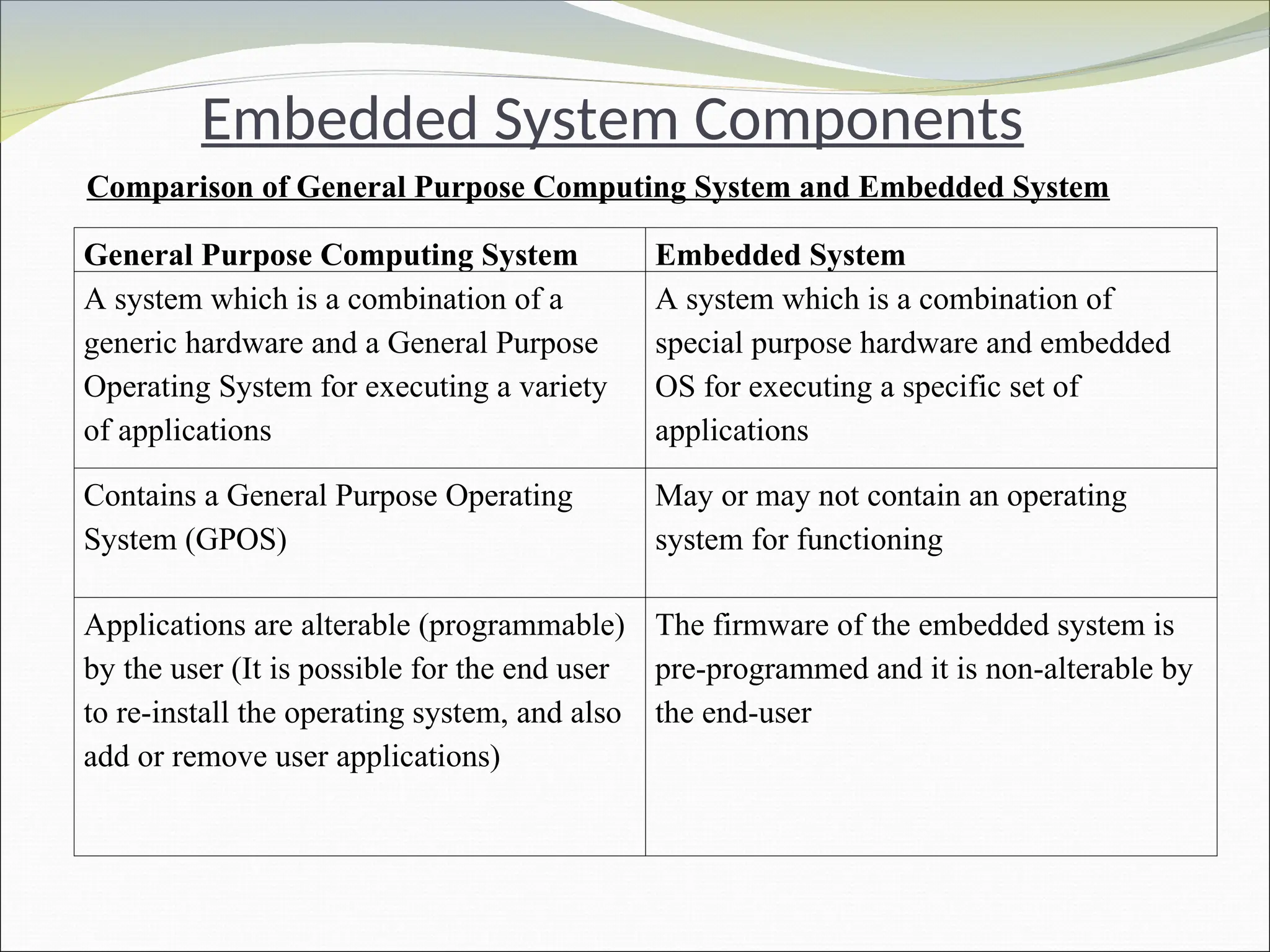
GeneralPurpose Computing System Embedded System
A system which is a combination of a
generic hardware and a General Purpose
Operating System for executing a variety
of applications
A system which is a combination of
special purpose hardware and embedded
OS for executing a specific set of
applications
Contains a General Purpose Operating
System (GPOS)
May or may not contain an operating
system for functioning
Applications are alterable (programmable)
by the user (It is possible for the end user
to re-install the operating system, and also
add or remove user applications)
The firmware of the embedded system is
pre-programmed and it is non-alterable by
the end-user
Comparison of General Purpose Computing System and Embedded System
3.
Embedded System Components
Parameter
GeneralPurpose Computing
System – Computer
Embedded System
Basic
A computer is a general purpose
electronic device used to perform
different types of tasks.
An embedded system is a
specialized computer system
that used to perform one or a
few specific tasks.
Purpose
Computers are used for
accomplishing general purpose
computing tasks.
Embedded systems are used
for accomplishing specific
tasks in a larger system.
System
hardware
A computer typically consists of a
CPU, storage unit, and I/O units.
Embedded system are
designed with a microcontroller
which consists of a CPU,
memory unit, and I/O interface
on a single IC chip.
Processing
power
Computers have very high
processing power.
Embedded systems have
relatively low processing
power.
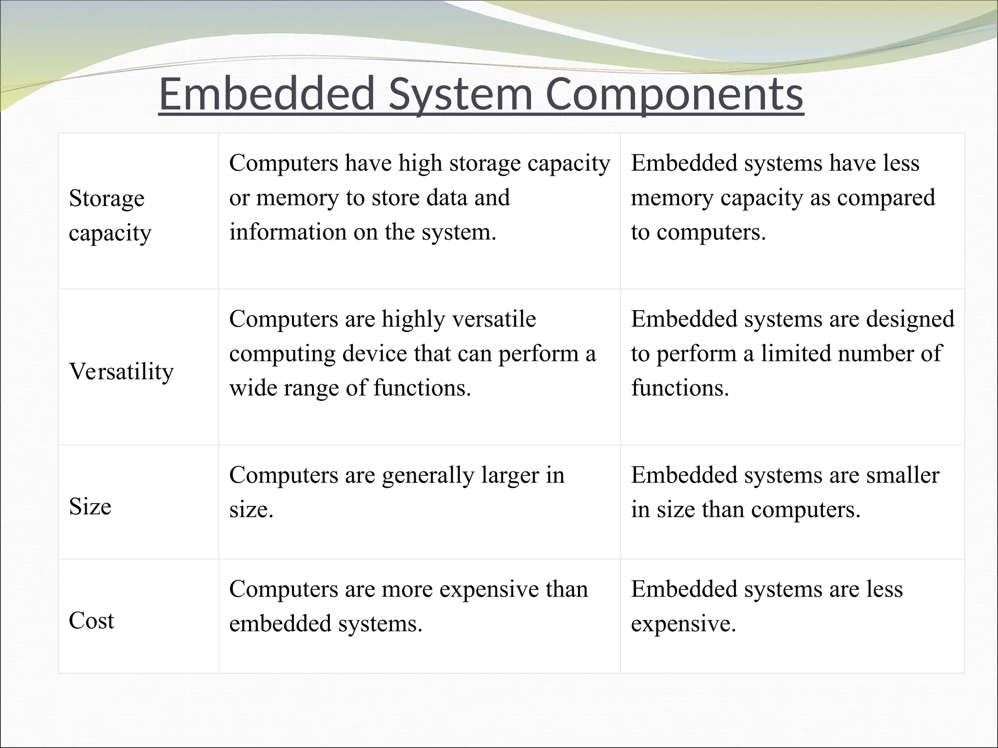
4.
Embedded System Components
Storage
capacity
Computershave high storage capacity
or memory to store data and
information on the system.
Embedded systems have less
memory capacity as compared
to computers.
Versatility
Computers are highly versatile
computing device that can perform a
wide range of functions.
Embedded systems are designed
to perform a limited number of
functions.
Size
Computers are generally larger in
size.
Embedded systems are smaller
in size than computers.
Cost
Computers are more expensive than
embedded systems.
Embedded systems are less
expensive.
5.
Embedded System Components
Operating
system
Computersuse a full-featured
operating system to run
Ex: Windows,Ubuntu,MAC
Os,Fedora ,Solaris, Chrome
OS,Cent OS,Debian
Embedded systems use a
specialized operating
system to run.
Ex: Linux,Vx works,Integrity
Human-
machine
interface
(HMI)
Computers have a human-
machine interface that allows
end-users to interact with the
computer.
Embedded systems
generally have a limited or
no human-machine
interface.
Software
developme
nt tools
For computers, the general
purpose development tools can
be used to develop computer
software.
The development of
software for embedded
systems requires
specialized and expert
tools. MATLAB , LABVIEW
6.
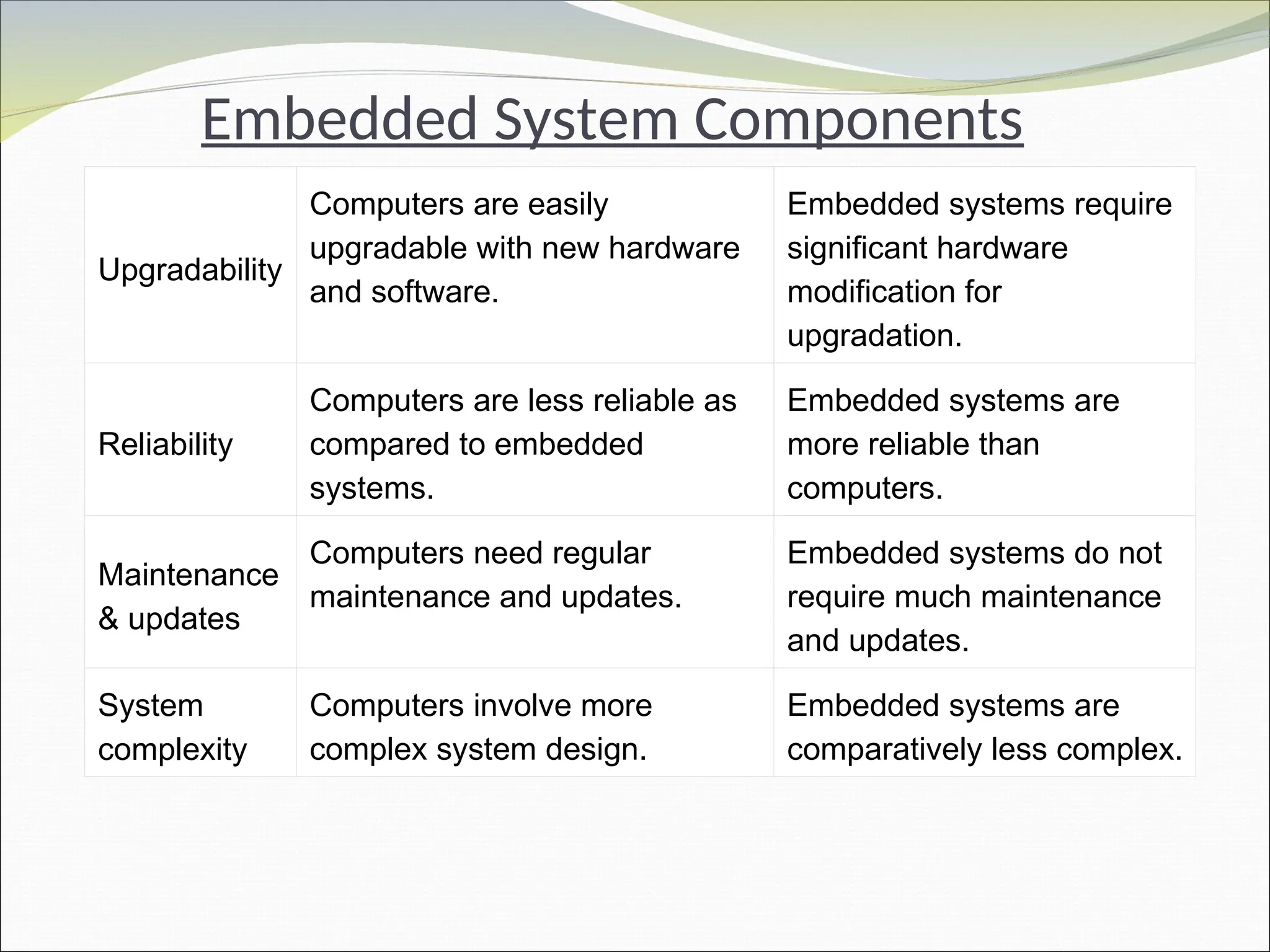
Embedded System Components
Upgradability
Computersare easily
upgradable with new hardware
and software.
Embedded systems require
significant hardware
modification for
upgradation.
Reliability
Computers are less reliable as
compared to embedded
systems.
Embedded systems are
more reliable than
computers.
Maintenance
& updates
Computers need regular
maintenance and updates.
Embedded systems do not
require much maintenance
and updates.
System
complexity
Computers involve more
complex system design.
Embedded systems are
comparatively less complex.
7.
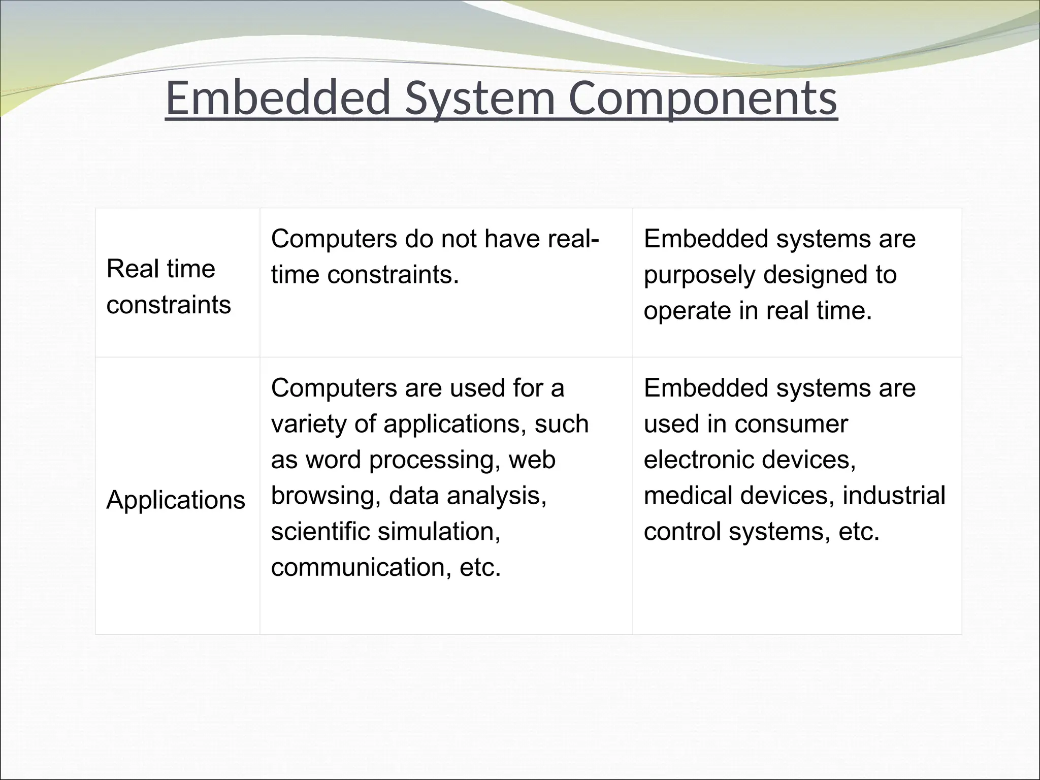
Embedded System Components
Realtime
constraints
Computers do not have real-
time constraints.
Embedded systems are
purposely designed to
operate in real time.
Applications
Computers are used for a
variety of applications, such
as word processing, web
browsing, data analysis,
scientific simulation,
communication, etc.
Embedded systems are
used in consumer
electronic devices,
medical devices, industrial
control systems, etc.
8.
History of Embeddedsystem
In 1960, embedded system was first used for
developing Apollo Guidance System – AGC –
Lunar Mission – in Moon -
The AGC provided computation and electronic
interfaces for guidance, navigation, and control
of the spacecraft.
Command Module (CM) and the Lunar Excursion
Module (LEM)
9.
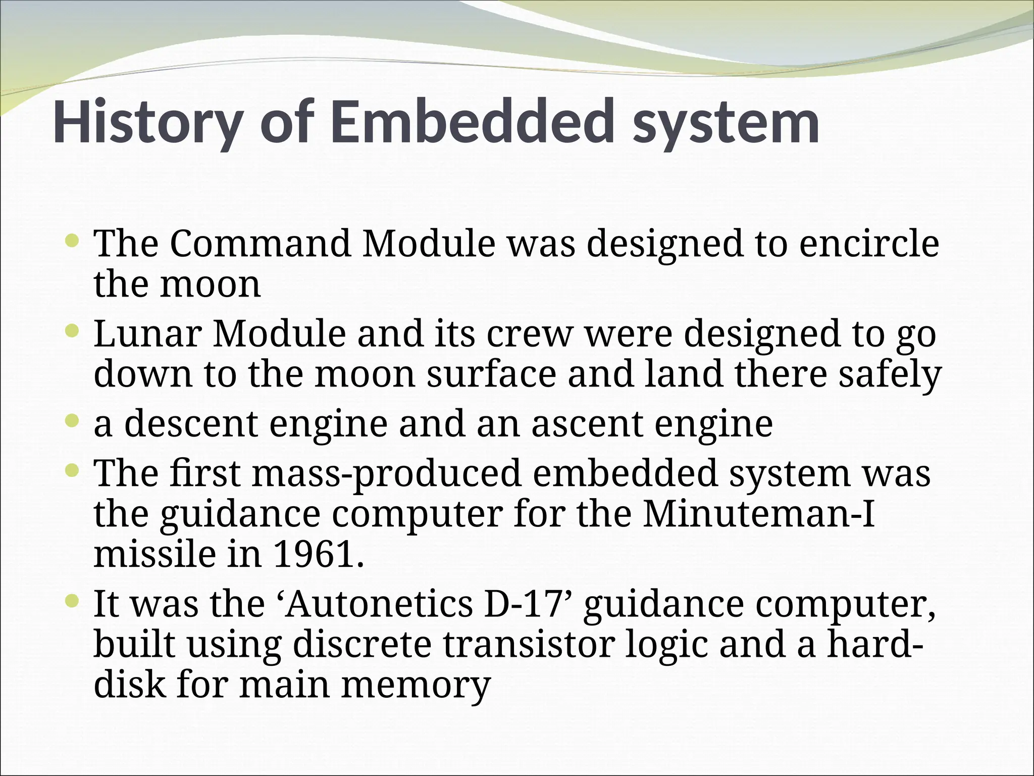
History of Embeddedsystem
The Command Module was designed to encircle
the moon
Lunar Module and its crew were designed to go
down to the moon surface and land there safely
a descent engine and an ascent engine
The first mass-produced embedded system was
the guidance computer for the Minuteman-I
missile in 1961.
It was the ‘Autonetics D-17’ guidance computer,
built using discrete transistor logic and a hard-
disk for main memory
10.
History of Embeddedsystem
In 1968, the first embedded system for a vehicle
was released.
Texas Instruments developed the first
microcontroller in 1971
In 1987, the first embedded OS, VxWorks, was
released by Wind River.
Microsoft’s Windows embedded CE in 1996.
By the late 1990s, the first embedded Linux
system appeared.
11.
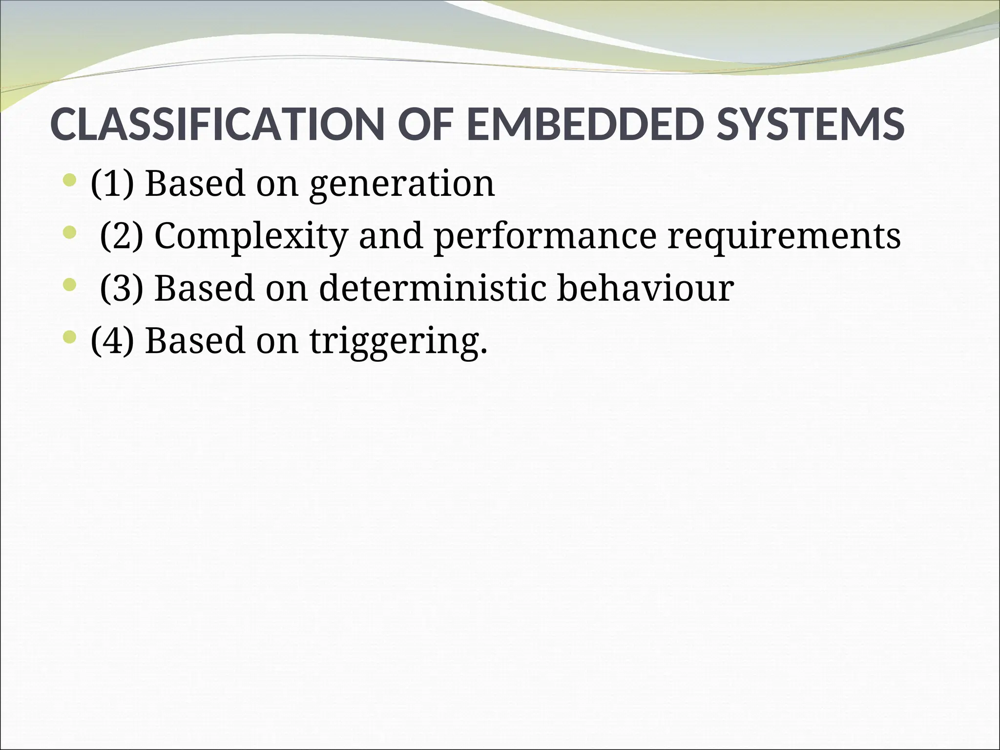
CLASSIFICATION OF EMBEDDEDSYSTEMS
(1) Based on generation
(2) Complexity and performance requirements
(3) Based on deterministic behaviour
(4) Based on triggering.
12.
CLASSIFICATION OF EMBEDDEDSYSTEMS
1.Classification Based on Generation
First Generation
The early embedded systems were built around
8bit microprocessors like 8085 and Z80, and 4bit
microcontrollers.
Simple in hardware circuits with firmware
developed in Assembly code.
Digital telephone keypads, stepper motor control
units etc. are examples of this.
13.
CLASSIFICATION OF EMBEDDEDSYSTEMS
Second Generation
These are embedded systems built around 16bit
microprocessors and 8 or 16 bit microcontrollers
The instruction set - more complex and powerful than
the first generation processors
contained embedded operating systems for their
operation
Ex :Data Acquisition Systems, SCADA systems
SCADA (supervisory control and data acquisition) is a category of software
applications for controlling industrial processes, which is the gathering of data in
real time from remote locations in order to control equipment and conditions
14.
CLASSIFICATION OF EMBEDDEDSYSTEMS
Third Generation
Powerful 32 bit processors and 16 bit
microcontrollers
Application and domain specific
processors/controllers like Digital Signal Processors
(DSP) and Application Specific Integrated Circuits
(ASICs) came into the picture
ASIC - is a chip on which the pattern of connections
has been set up exclusively for a specific function.
15.
CLASSIFICATION OF EMBEDDEDSYSTEMS
Fourth Generation
System on Chips (SoC)
It is an integrated circuit that integrates most or all
components of a computer or other electronic system
Reconfigurable processors
A computer architecture that facilitates faster & more
complex computing to process data
multicore processors
Above are bringing high performance, miniaturisation
into the embedded device market
Ex : Smart phone devices, mobile internet devices (MIDs)
16.
CLASSIFICATION OF EMBEDDEDSYSTEMS
2. Classifi cation Based on Complexity and
Performance
(i)Small-Scale Embedded Systems
Embedded systems which are simple in
application needs and the performance
requirements are not time critical
Low performance and low cost 8 or 16 bit
microprocessors/microcontrollers
May or may not contain OS
Ex - An electronic toy
17.
CLASSIFICATION OF EMBEDDEDSYSTEMS
2. Classifi cation Based on Complexity and
Performance
(ii) Medium-Scale Embedded Systems
Embedded systems which are slightly complex in
hardware and firmware (software) requirements
medium performance, low cost 16 or 32 bit
microprocessors/microcontrollers or digital signal
processors
contain an embedded operating system
18.
CLASSIFICATION OF EMBEDDEDSYSTEMS
2. Classification Based on Complexity and
Performance
(iii)Large-Scale Embedded Systems/Complex
Systems Embedded systems
Involve highly complex hardware and fi rmware
requirements
Employed in mission critical applications
High performance
Built in 32 or 64 bit RISC processors/controllers or
Reconfigurable System on Chip ( RSoC) or multi-core
processors
Decoding/ encoding of media, cryptographic function
19.
MAJOR APPLICATION AREASOF EMBEDDED SYSTEMS
(1)Consumer electronics: Camcorders, cameras, etc.
(2) Household appliances: Television, DVD players,
washing machine, fridge, microwave oven, etc.
(3) Home automation and security systems: Air
conditioners, sprinklers, intruder detection alarms,
closed circuit television cameras, fi re alarms, etc.
(4) Automotive industry: Anti-lock breaking systems
(ABS), engine control, ignition systems, automatic
navigation systems, etc
20.
MAJOR APPLICATION AREASOF EMBEDDED SYSTEMS
(5) Telecom: Cellular telephones, telephone switches,
handset multimedia applications, etc.
(6) Computer peripherals: Printers, scanners, fax
machines, etc.
(7) Computer networking systems: Network routers,
switches, hubs, fi rewalls, etc.
(8) Healthcare: Different kinds of scanners, EEG, ECG
machines etc.
(9) Measurement & Instrumentation: Digital multimeters,
digital CROs, logic analysers PLC systems, etc.
(10) Banking & Retail: Automatic teller machines (ATM)
and currency counters, point of sales (POS)
21.
MAJOR APPLICATION AREASOF EMBEDDED SYSTEMS
(11) Card Readers: Barcode, smart card readers, hand
held devices, etc.
(12) Wearable Devices: Health and Fitness Trackers,
Smartphone Screen extension for notifi cations, etc.
(13) Cloud Computing and Internet of Things (IOT)
22.
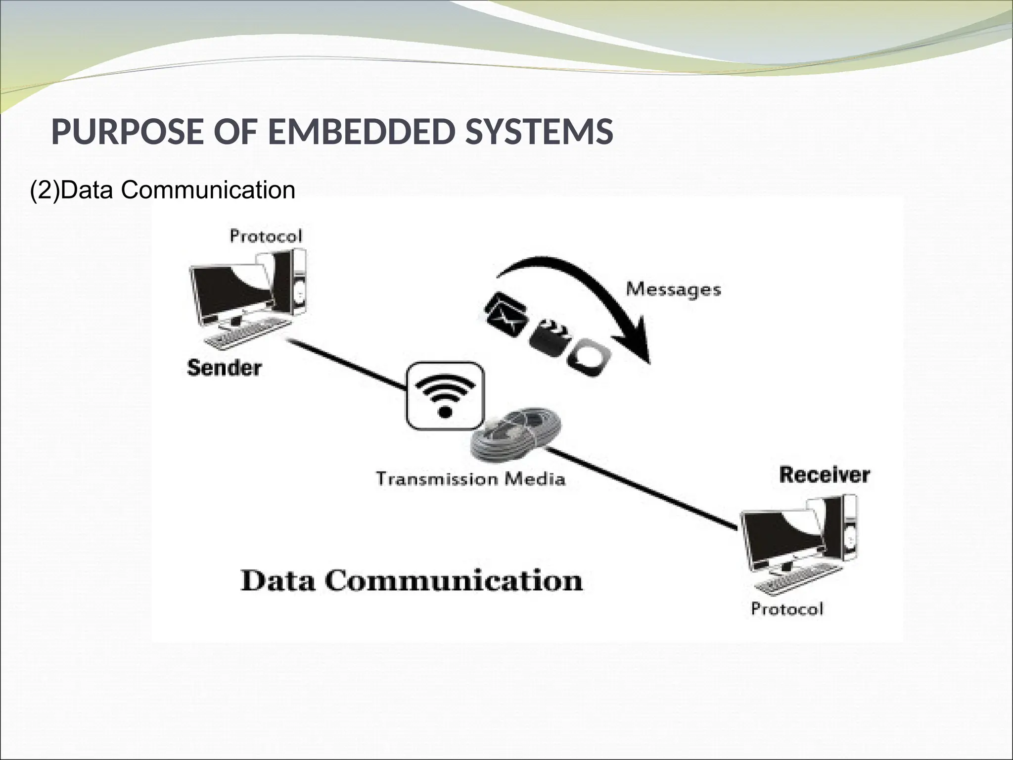
PURPOSE OF EMBEDDEDSYSTEMS
PURPOSE OF EMBEDDED SYSTEMS
(1)Data collection/Storage/Representation
(2) Data communication
(3) Data (signal) processing
(4) Monitoring
(5) Control
(6) Application specifi c user interface
23.
(1)Data collection/Storage/Representation
Embeddedsystems designed for the purpose of data
collection performs acquisition of data from the
external world.
Data collection is usually done for storage, analysis,
manipulation, and transmission.
The term “data” refers to all kinds of information,
viz. text, voice, image, video, electrical signals and
any other measurable quantities.
Data can be either analog (continuous) or digital
(discrete).
PURPOSE OF EMBEDDED SYSTEMS
24.
(1)Data collection/Storage/Representation
Embeddedsystems with analog data capturing
techniques collect data directly in the form of analog
signals
Embedded systems with digital data collection
mechanism converts the analog signal to
corresponding digital signal using analog to digital
(A/D) converters and then collects the binary
equivalent of the analog data.
If the data is digital, it can be directly captured
without any additional interface by digital embedded
systems
PURPOSE OF EMBEDDED SYSTEMS
25.
PURPOSE OF EMBEDDEDSYSTEMS
(1)Data collection/Storage/Representation
The collected data may be stored directly in the
system
or
may be transmitted to some other systems
or
it may be processed by the system
or
it may be deleted instantly after giving a
meaningful representation.
26.
PURPOSE OF EMBEDDEDSYSTEMS
(1)Data collection/Storage/Representation
Embedded systems designed for pure measurement
applications without storage used in control and
instrumentation domain,
collects data and gives a meaningful representation
of the collected data by means of graphical
representation or quantity value and deletes the
collected data when new data arrives at the data
collection terminal.
Analog and digital CROs without storage memory
are typical examples of this.
27.
PURPOSE OF EMBEDDEDSYSTEMS
(1)Data collection/Storage/Representation
Examples :
Central heating systems
GPS systems
Fitness trackers
Medical devices
Automotive systems
28.
PURPOSE OF EMBEDDEDSYSTEMS
Data Communication
Embedded data communication systems are
deployed in applications ranging from complex
satellite communication systems to simple home
networking systems.
The transmission is achieved either by a wire-line
medium or by a wireless medium.
Wireline medium was the most common choice in
all olden days embedded systems
PURPOSE OF EMBEDDEDSYSTEMS
(2)Data Communication
Sender – Channel – Receiver
A wireless medium offers cheaper connectivity
solutions and make the communication link free
from the hassle of wire bundles.
Data can either be transmitted by analog means or
by digital means.
Modern industry trends are settling towards digital
communication
31.
PURPOSE OF EMBEDDEDSYSTEMS
Data Communication
The data collecting embedded terminal itself can
incorporate data communication units like
wireless modules (Bluetooth, ZigBee, Wi-Fi, EDGE,
GPRS, etc.)
or
wire-line modules (RS232C, USB, TCP/IP -
Transmission Control Protocol – Internet Protocol)
32.
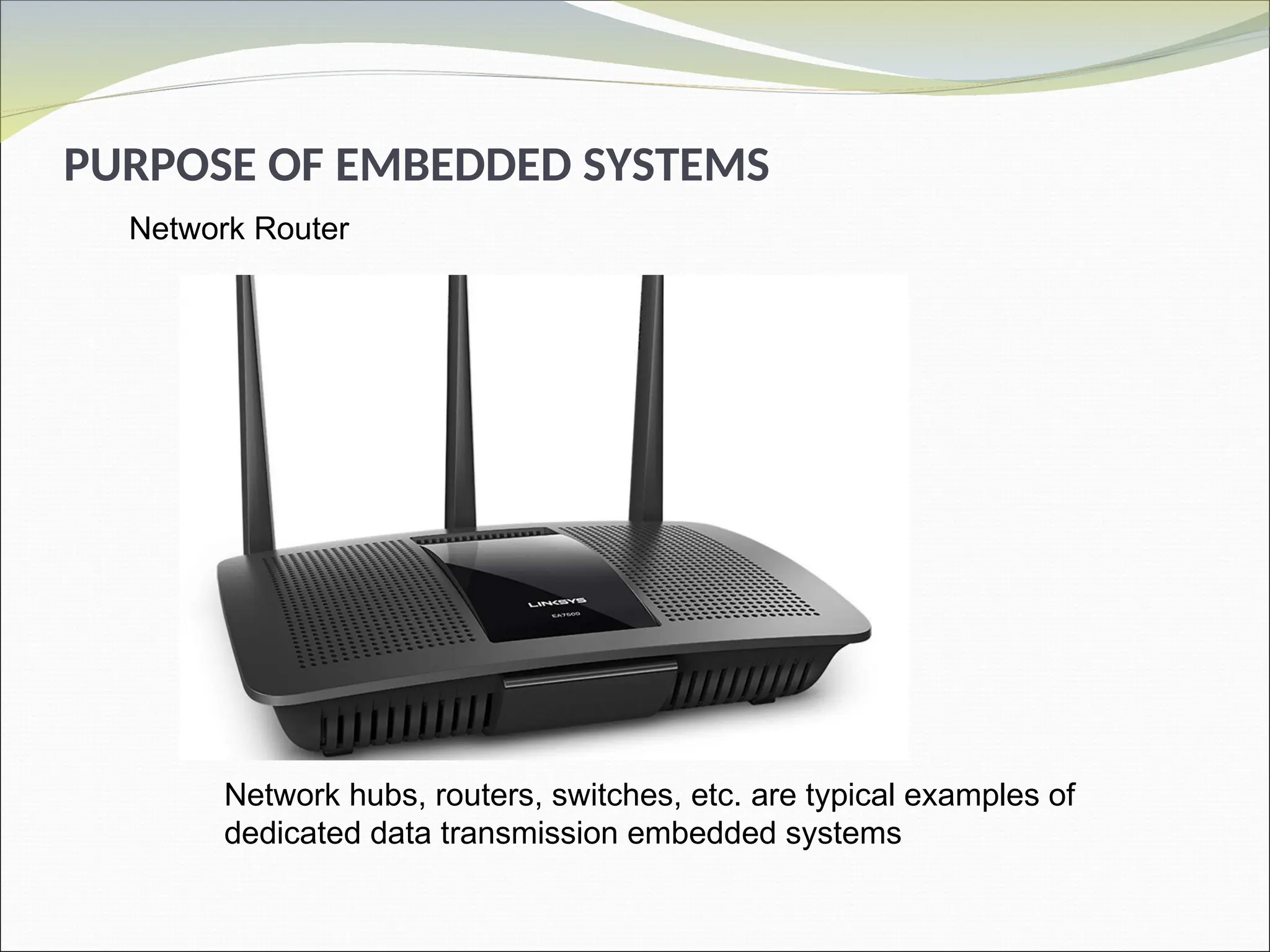
PURPOSE OF EMBEDDEDSYSTEMS
Network Router
Network hubs, routers, switches, etc. are typical examples of
dedicated data transmission embedded systems
33.
PURPOSE OF EMBEDDEDSYSTEMS
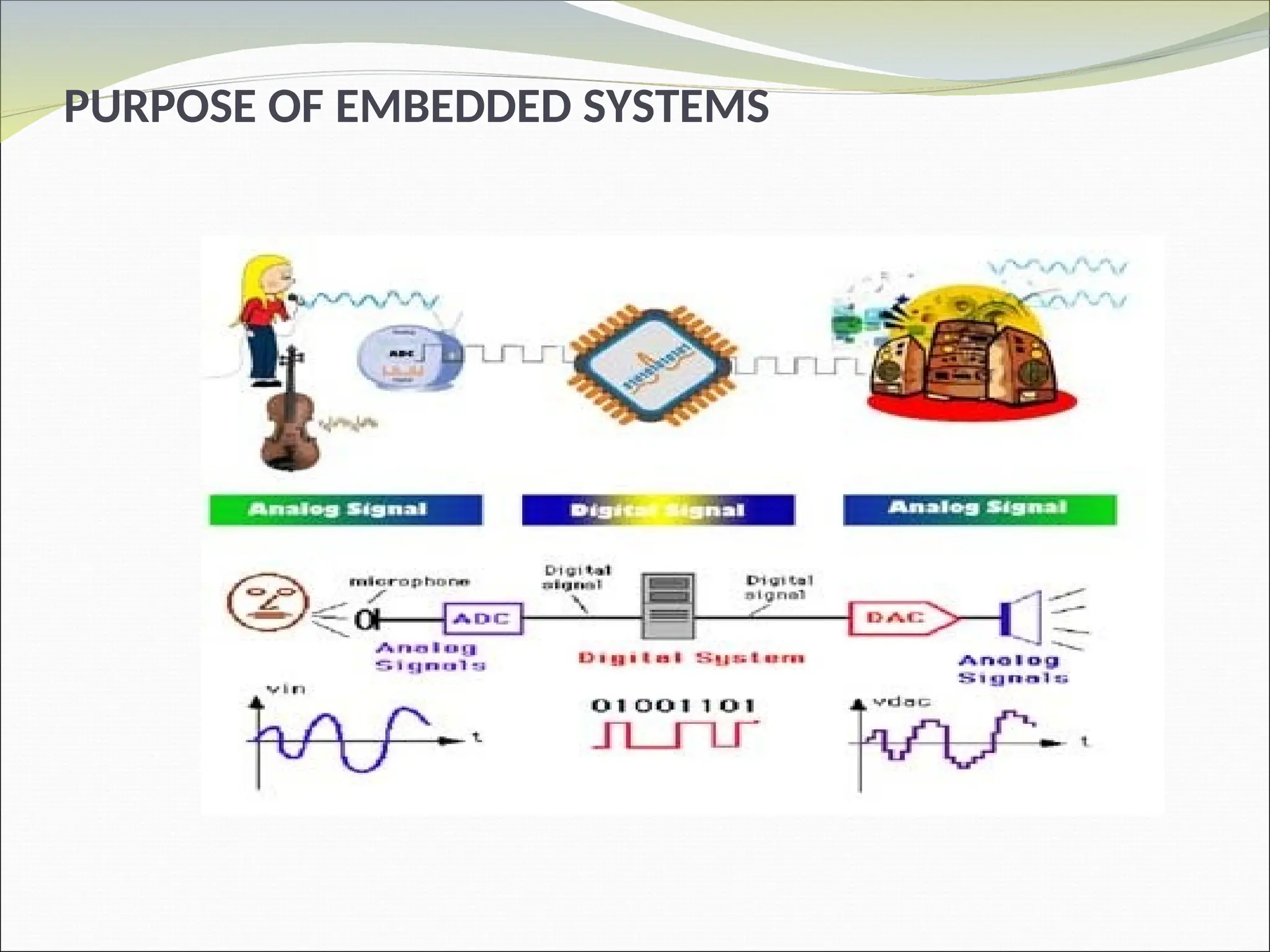
(3)Data (Signal) Processing
The data (voice, image, video, electrical signals,
and other measurable quantities) collected by
embedded systems may be used for various
kinds of data processing.
Embedded systems with signal processing
functionalities are employed in applications
demanding signal processing like speech coding,
synthesis, audio video codec, transmission
applications, etc.
34.
PURPOSE OF EMBEDDEDSYSTEMS
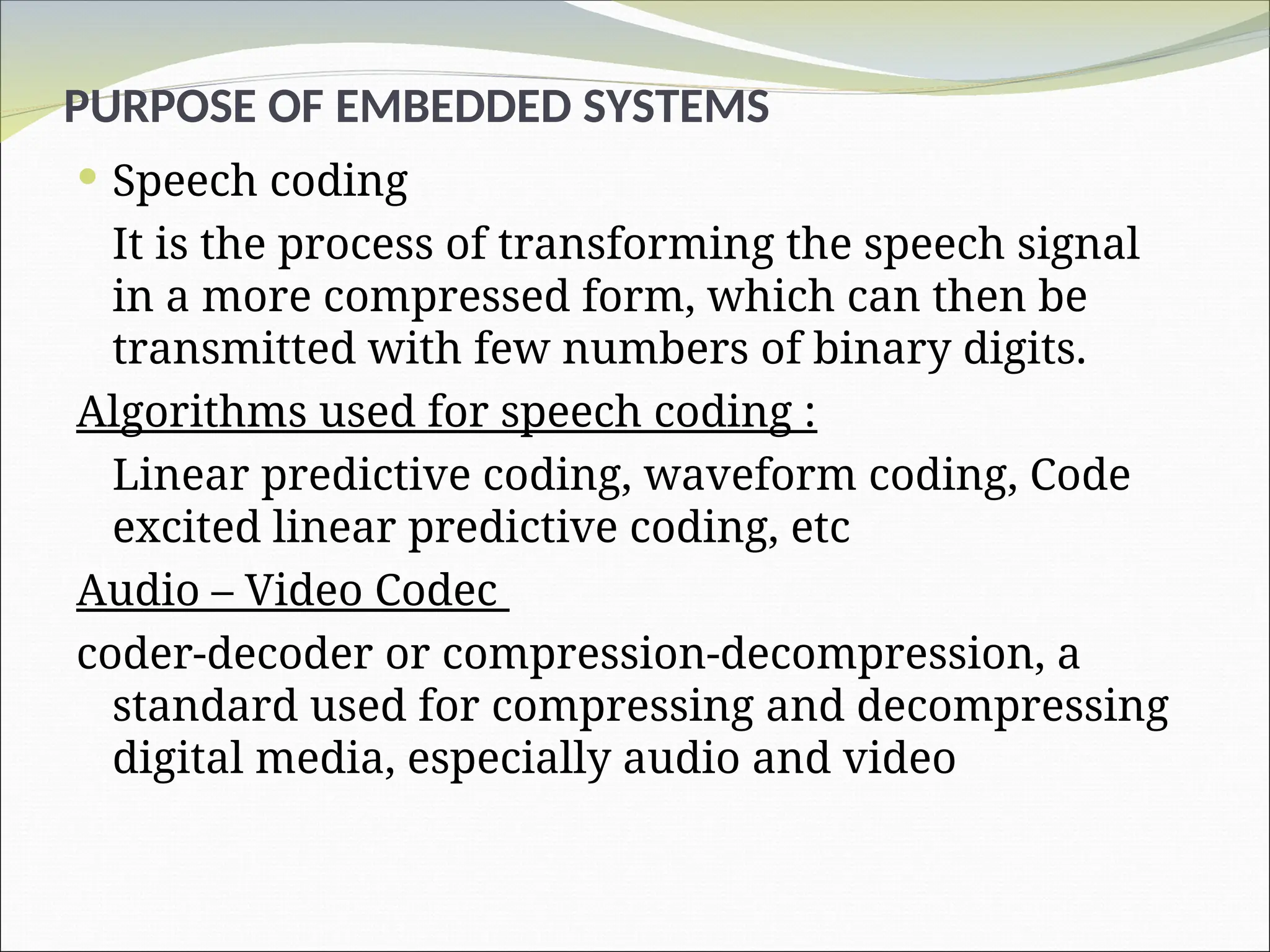
Speech coding
It is the process of transforming the speech signal
in a more compressed form, which can then be
transmitted with few numbers of binary digits.
Algorithms used for speech coding :
Linear predictive coding, waveform coding, Code
excited linear predictive coding, etc
Audio – Video Codec
coder-decoder or compression-decompression, a
standard used for compressing and decompressing
digital media, especially audio and video
PURPOSE OF EMBEDDEDSYSTEMS
(4)Monitoring
Embedded systems falling under this category are
specifically designed for monitoring purpose.
Almost all embedded products coming under the
medical domain are with monitoring functions
only
A very good example is the electro cardiogram
(ECG) machine for monitoring the heartbeat of a
patient.
The machine is intended to do the monitoring of
the heartbeat.
It cannot impose control over the heartbeat
37.
PURPOSE OF EMBEDDEDSYSTEMS
(4)Monitoring
The sensors used in ECG are the different
electrodes connected to the patient’s body.
Some other examples of embedded systems with
monitoring function are measuring instruments
like digital CRO, digital multimeters, logic
analysers, etc. used in Control & Instrumentation
applications.
They are used for knowing (monitoring) the
status of some variables like current, voltage, etc.
They cannot control the variables in turn.
38.
PURPOSE OF EMBEDDEDSYSTEMS
(5)Control
Embedded systems with control functionalities
impose control over some variables according to
the changes in input variables.
A system with control functionality contains both
sensors and actuators.
Sensors are connected to the input port for
capturing the changes in environmental variable
or measuring variable.
The actuators connected to the output port are
controlled according to the changes in input
variable
39.
PURPOSE OF EMBEDDEDSYSTEMS
(5)Control
An actuator is a device that produces a motion
by converting energy and signals going into the
system
An actuator is a machine component that is used
for moving and controlling a system or
mechanism
Stepper Motor
AC Motor
Hydraulic Motor – according to hydraulic
pressure of liquid - movements
40.
PURPOSE OF EMBEDDEDSYSTEMS
(5)Control
Air conditioner system used in our home to
control the room temperature to a specifi ed
limit is a typical example for embedded system
for control purpose
Thermistor – Temp. – ON/OFF
The air compressor unit acts as the actuator.
The compressor is controlled according to the
current room temperature and the desired
temperature set by the end user
41.
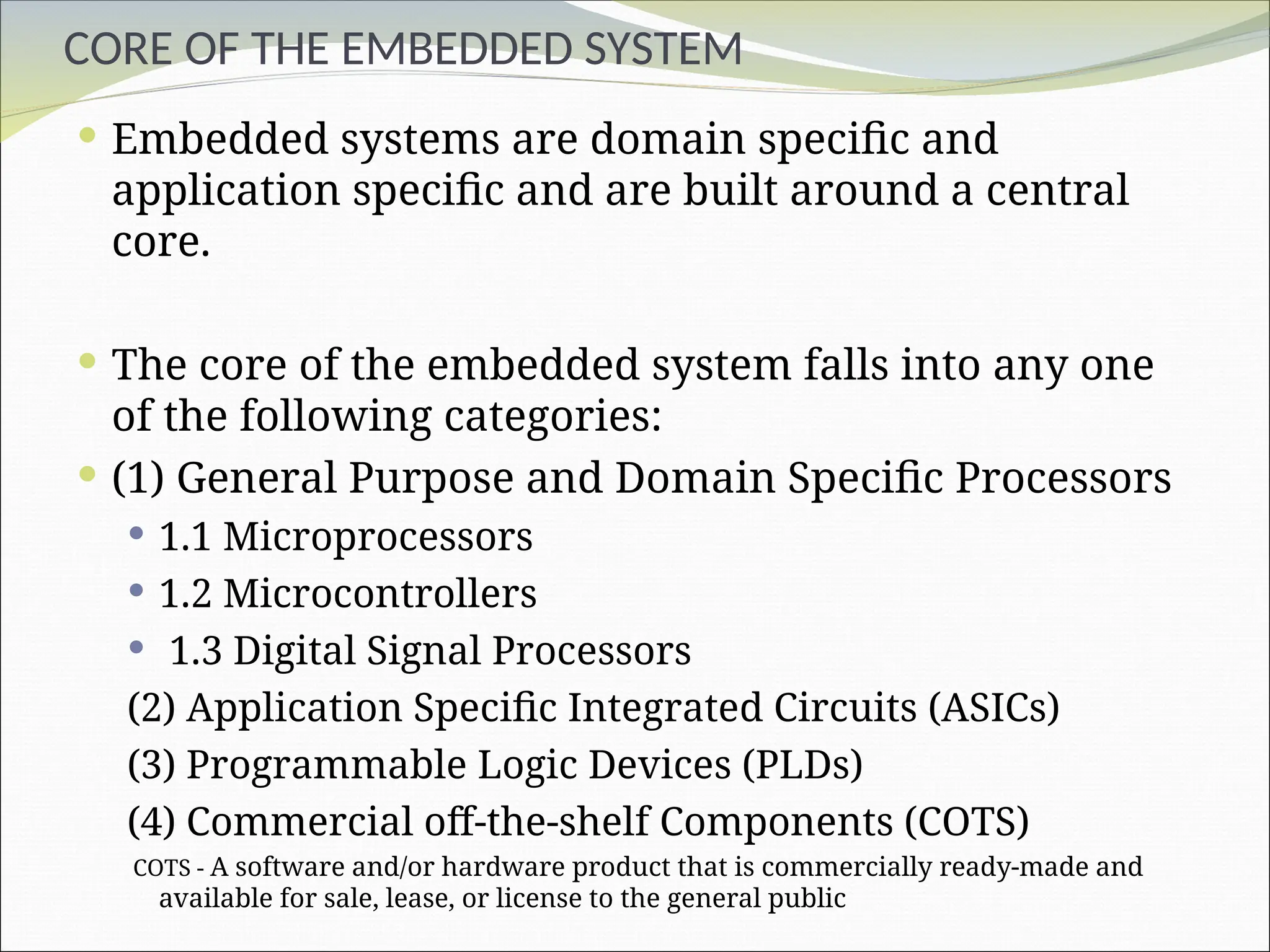
CORE OF THEEMBEDDED SYSTEM
Embedded systems are domain specific and
application specific and are built around a central
core.
The core of the embedded system falls into any one
of the following categories:
(1) General Purpose and Domain Specific Processors
1.1 Microprocessors
1.2 Microcontrollers
1.3 Digital Signal Processors
(2) Application Specific Integrated Circuits (ASICs)
(3) Programmable Logic Devices (PLDs)
(4) Commercial off-the-shelf Components (COTS)
COTS - A software and/or hardware product that is commercially ready-made and
available for sale, lease, or license to the general public
42.
CORE OF THEEMBEDDED SYSTEM
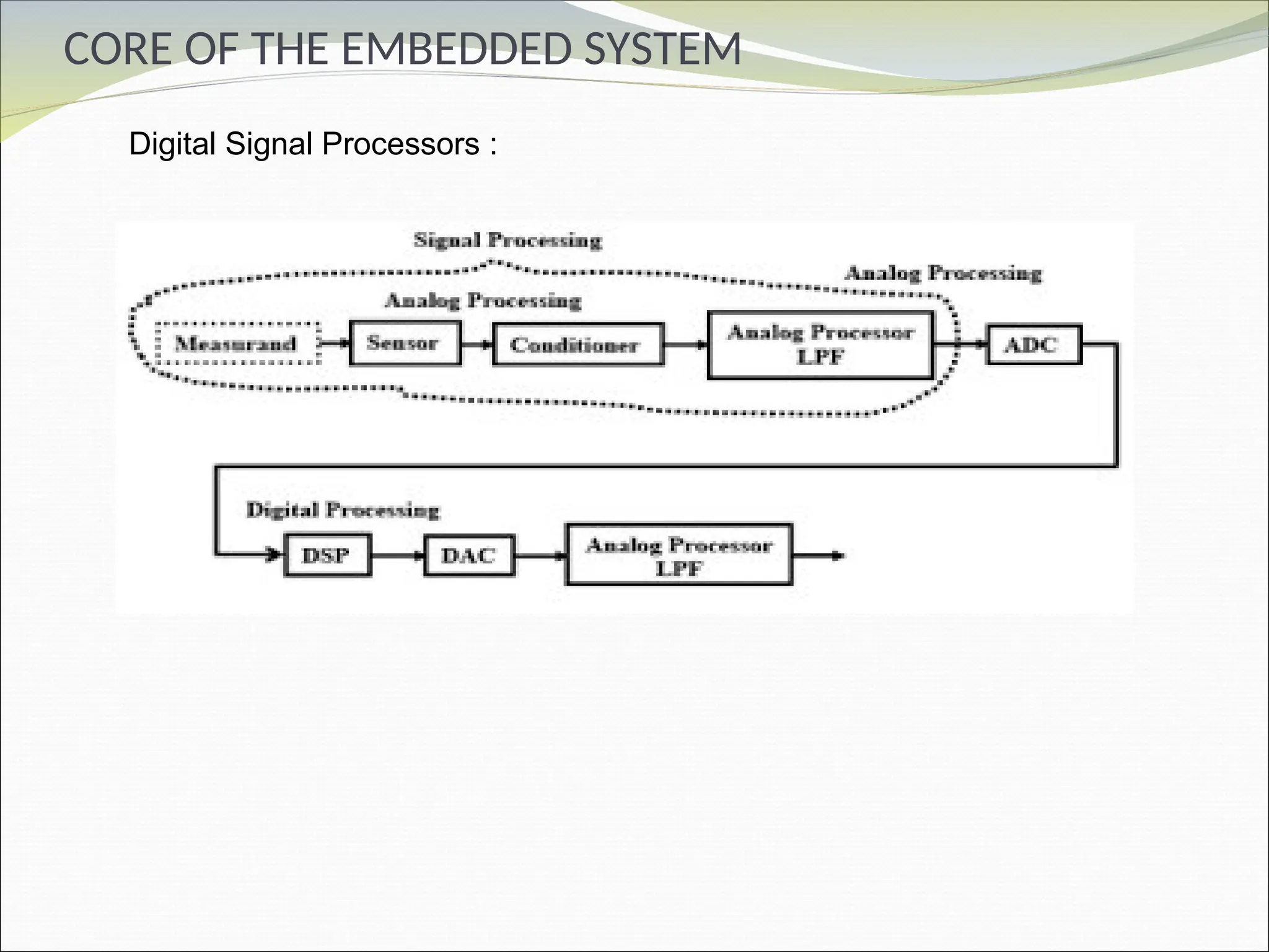
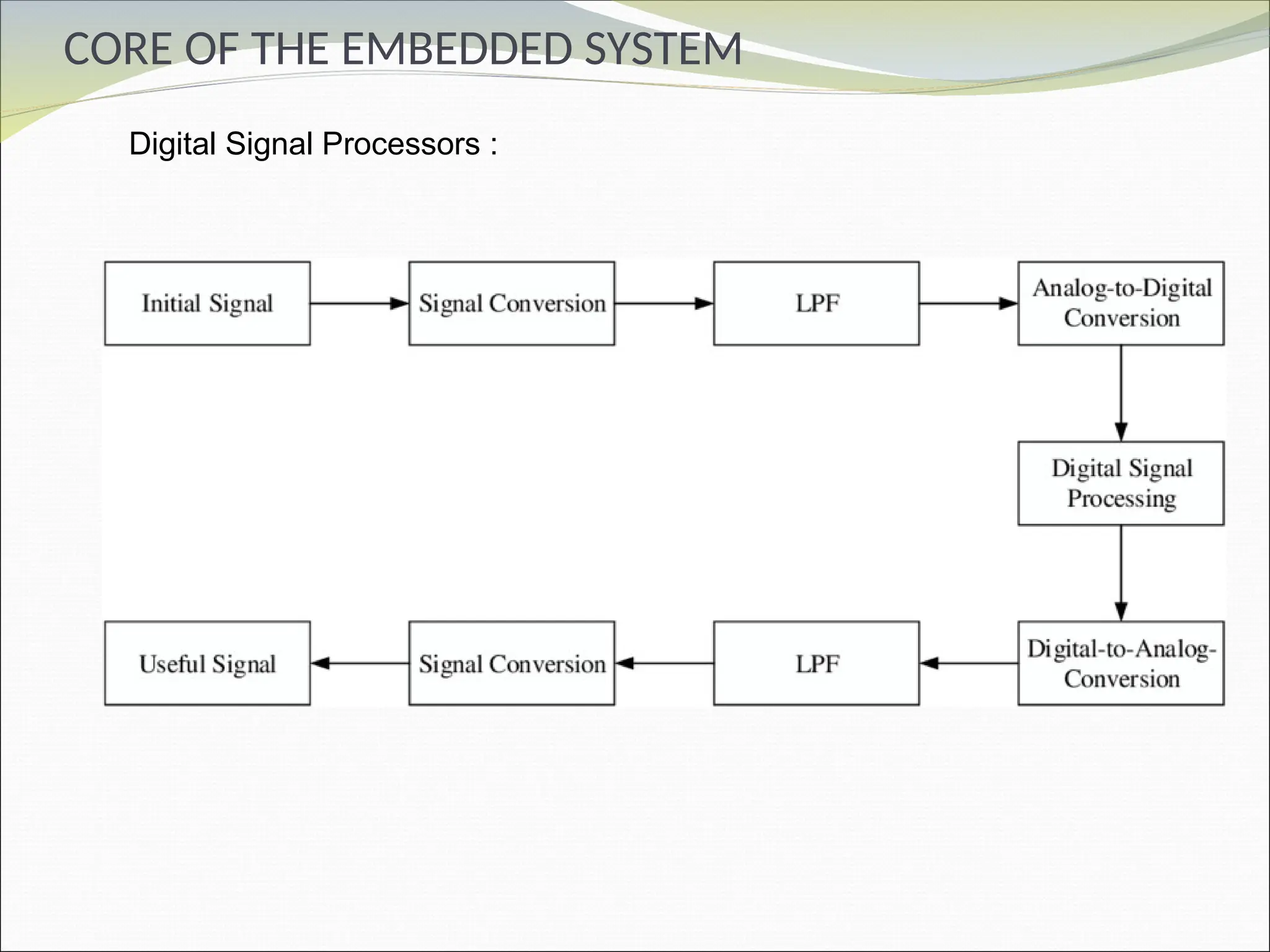
Digital Signal Processors :
43.
CORE OF THEEMBEDDED SYSTEM
Digital Signal Processors :
44.
CORE OF THEEMBEDDED SYSTEM
Digital Signal Processors :
Digital signal processors are 2 to 3 times faster than
the general purpose microprocessors in signal
processing applications.
DSPs implement algorithms in hardware which
speeds up the execution
But general purpose processors implement the
algorithm in firmware and the speed of execution
depends primarily on the clock (clock freq = 1 / Time
Duration) for the processors
45.
CORE OF THEEMBEDDED SYSTEM
Digital Signal Processors :
DSP has program memory, data memory,
computational engine (Performs the signal
processing in accordance with the stored program
memory) , I/O Unit
Audio video signal processing, telecommunication,
and multimedia applications are typical examples
where DSP is employed.
Digital signal processing employs a large amount of
real-time calculations. Sum of products (SOP)
calculation, convolution, fast fourier transform (FFT),
discrete fourier transform (DFT), etc, are some of the
operations performed by digital signal processors
46.
CORE OF THEEMBEDDED SYSTEM
Big-Endian Vs. Little-Endian
Processors/Controllers:
Endianness specifies the order in which the data
is stored in the memory by processor operations
in a multibyte system ( byte - eight bits)
Little-endian :
Little-endian means the lower-order byte of the data
is stored in memory at the lowest address, and the
higher-order byte at the highest address
47.
CORE OF THEEMBEDDED SYSTEM
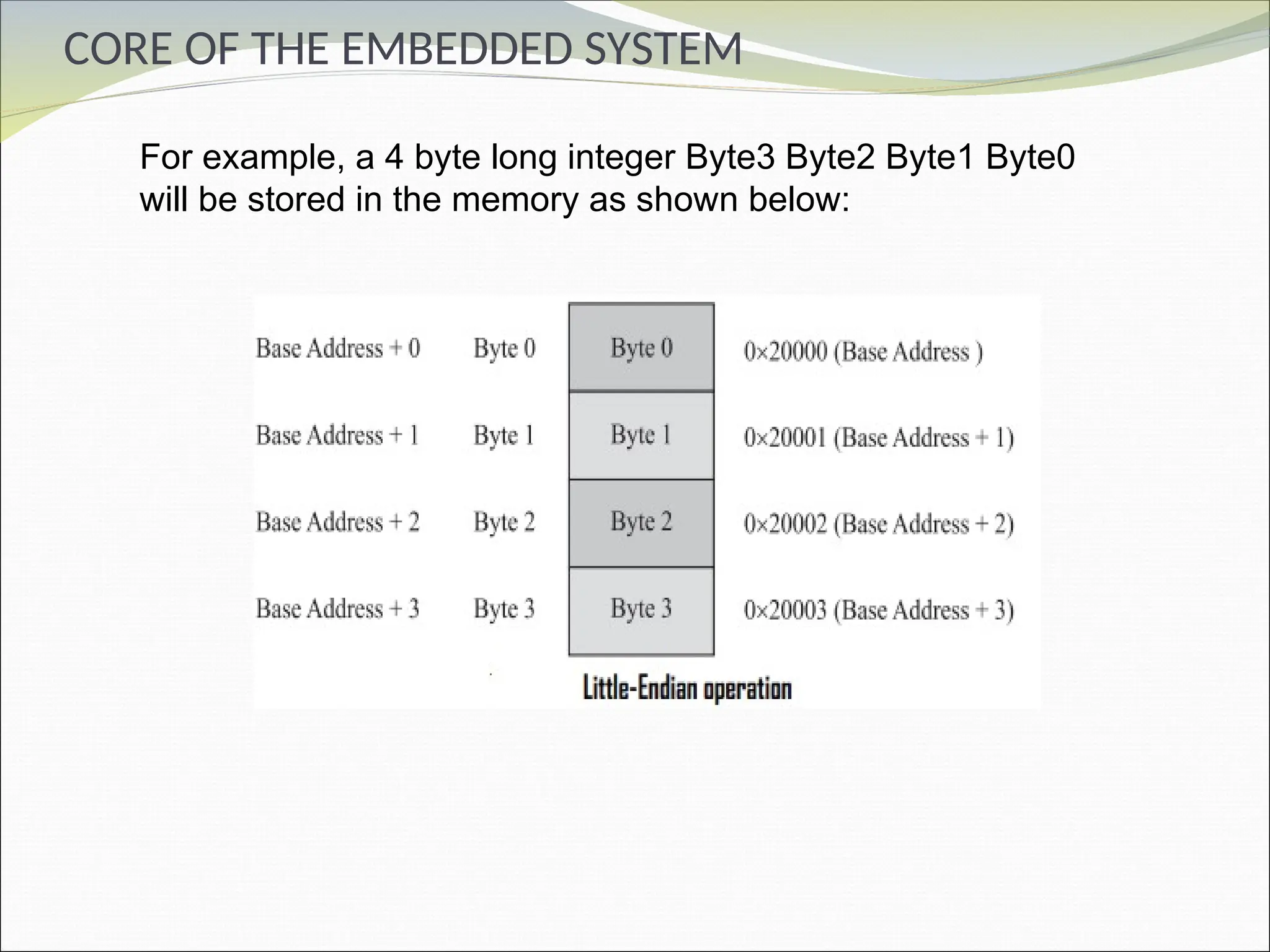
For example, a 4 byte long integer Byte3 Byte2 Byte1 Byte0
will be stored in the memory as shown below:
48.
CORE OF THEEMBEDDED SYSTEM
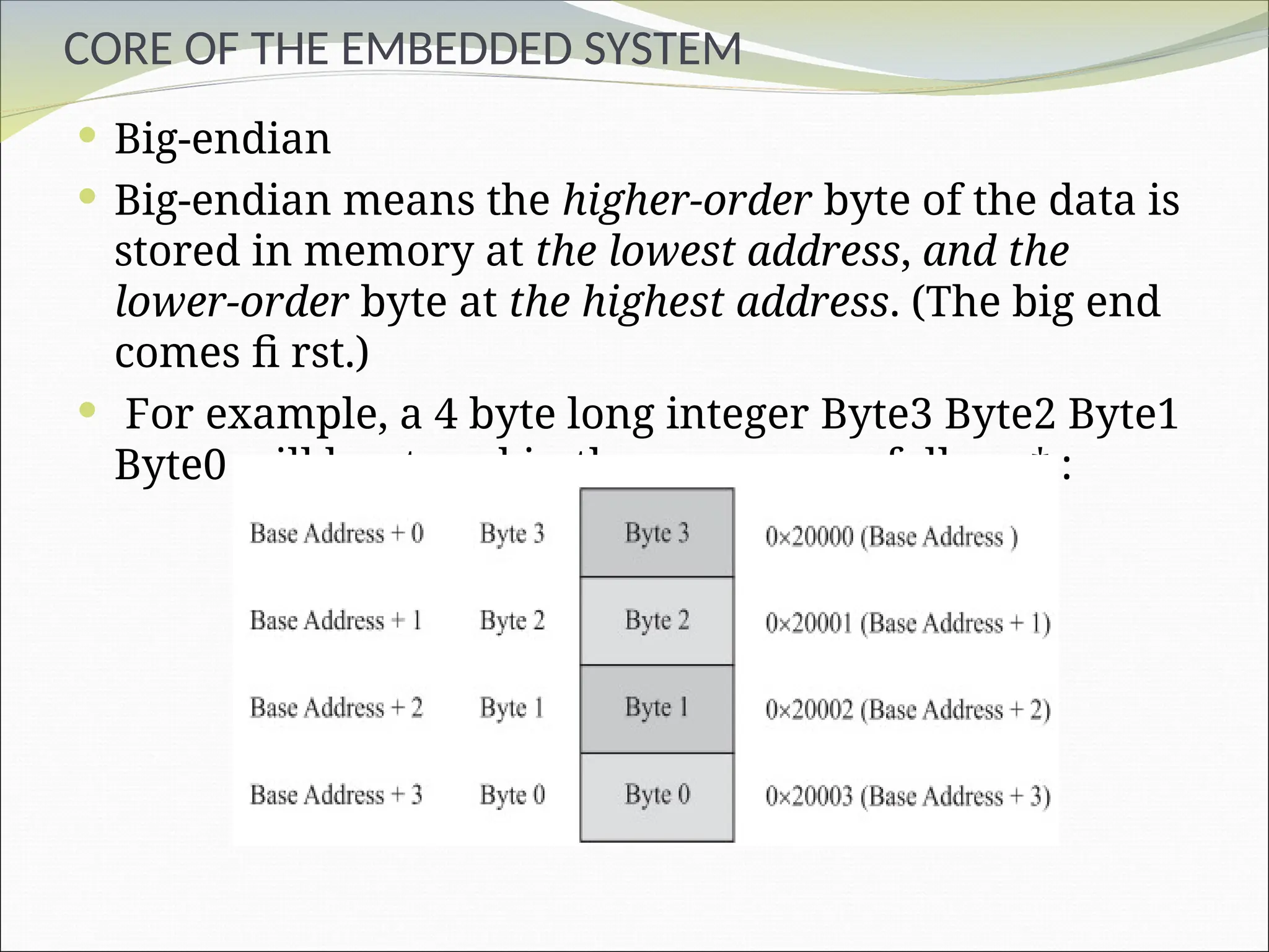
Big-endian
Big-endian means the higher-order byte of the data is
stored in memory at the lowest address, and the
lower-order byte at the highest address. (The big end
comes fi rst.)
For example, a 4 byte long integer Byte3 Byte2 Byte1
Byte0 will be stored in the memory as follows‡ :
49.
CORE OF THEEMBEDDED SYSTEM
Load Store Operation and Instruction Pipelining :
The memory access related operations are
performed by the special instructions load and store.
The content of memory location is loaded to a
register using the load instruction.
The instruction store stores data from a specifi ed
register to a specified memory location
50.
CORE OF THEEMBEDDED SYSTEM
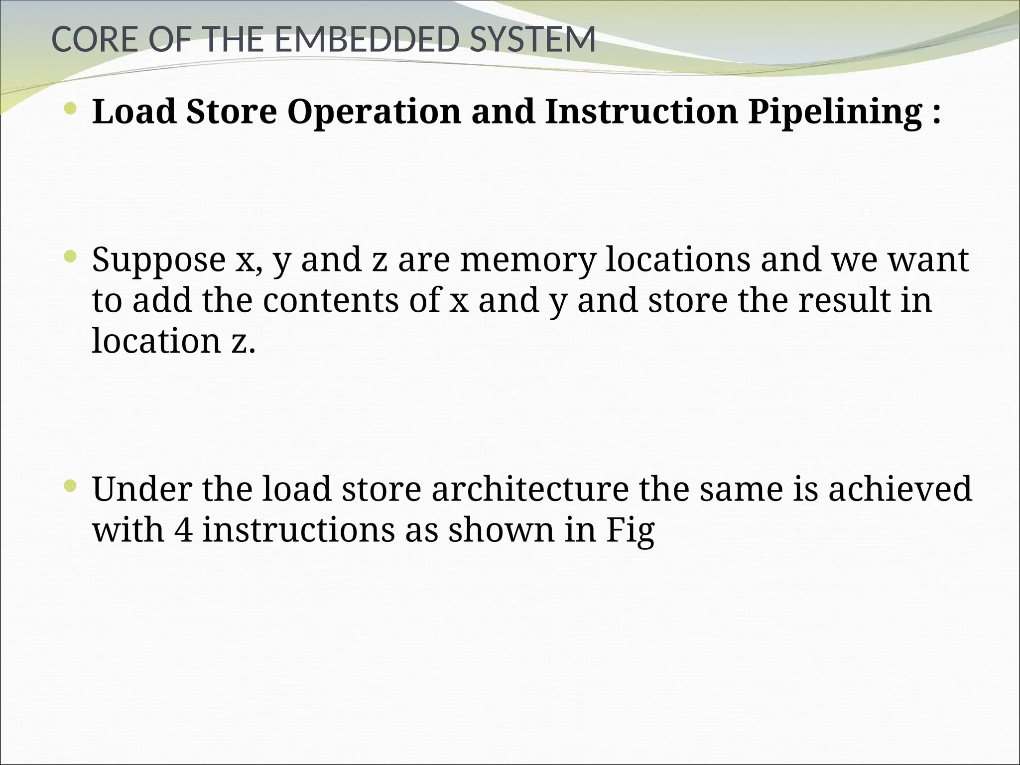
Load Store Operation and Instruction Pipelining :
Suppose x, y and z are memory locations and we want
to add the contents of x and y and store the result in
location z.
Under the load store architecture the same is achieved
with 4 instructions as shown in Fig
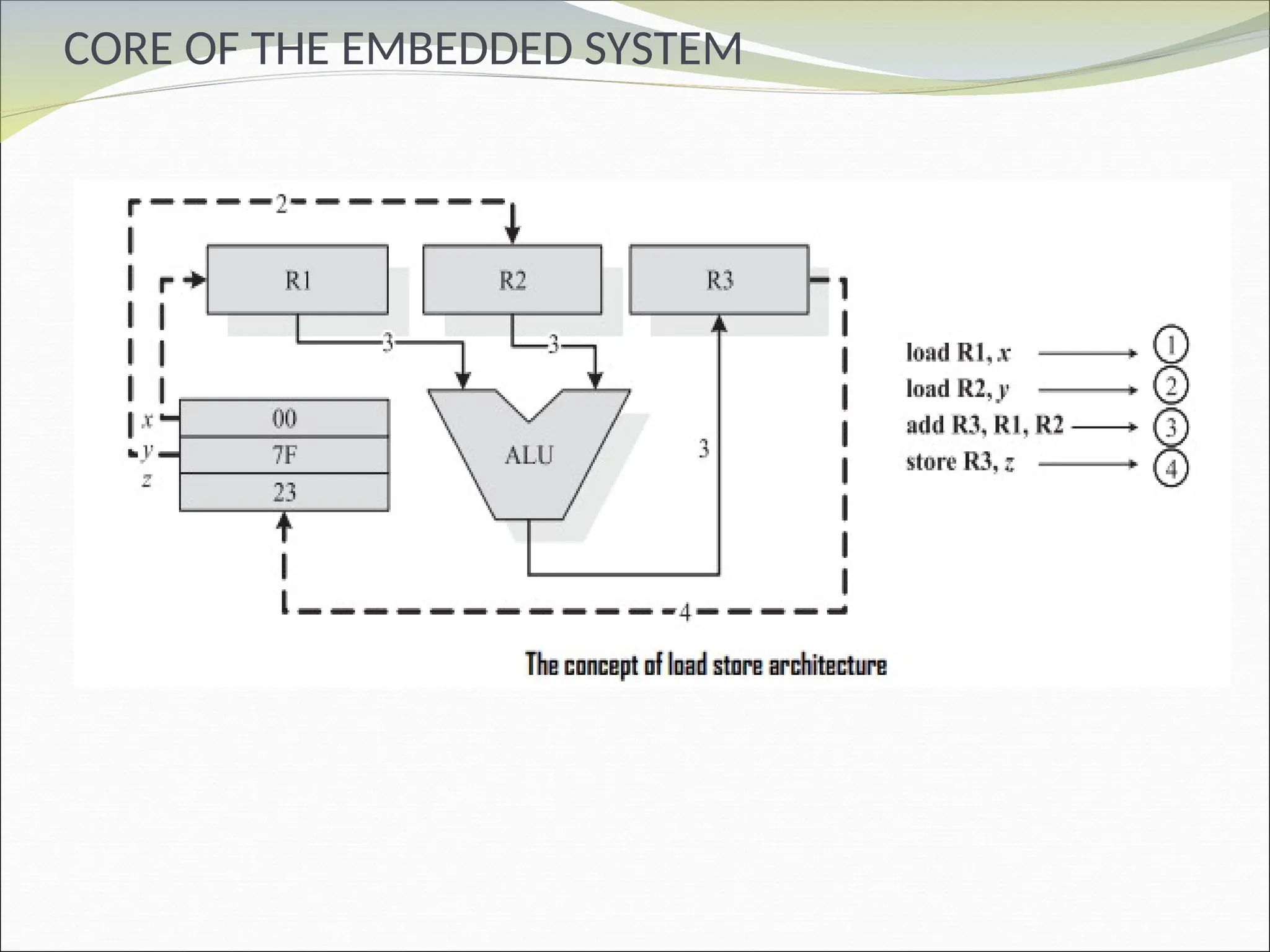
CORE OF THEEMBEDDED SYSTEM
Load Store Operation and Instruction Pipelining :
The fi rst instruction load R1, x loads the register R1
with the content of memory location x
The second instruction load R2,y loads the register R2
with the content of memory location y.
The instruction add R3, R1, R2 adds the content of
registers R1 and R2 and stores the result in register R3.
The next instruction store R3,z stores the content of
register R3 in memory location z
53.
CORE OF THEEMBEDDED SYSTEM
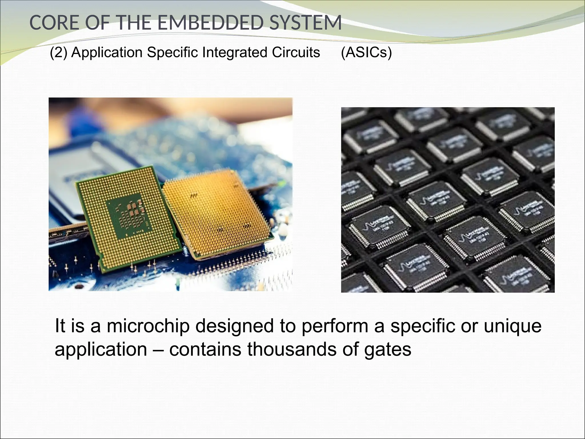
(2) Application Specific Integrated Circuits (ASICs)
It is a microchip designed to perform a specific or unique
application – contains thousands of gates
54.
CORE OF THEEMBEDDED SYSTEM
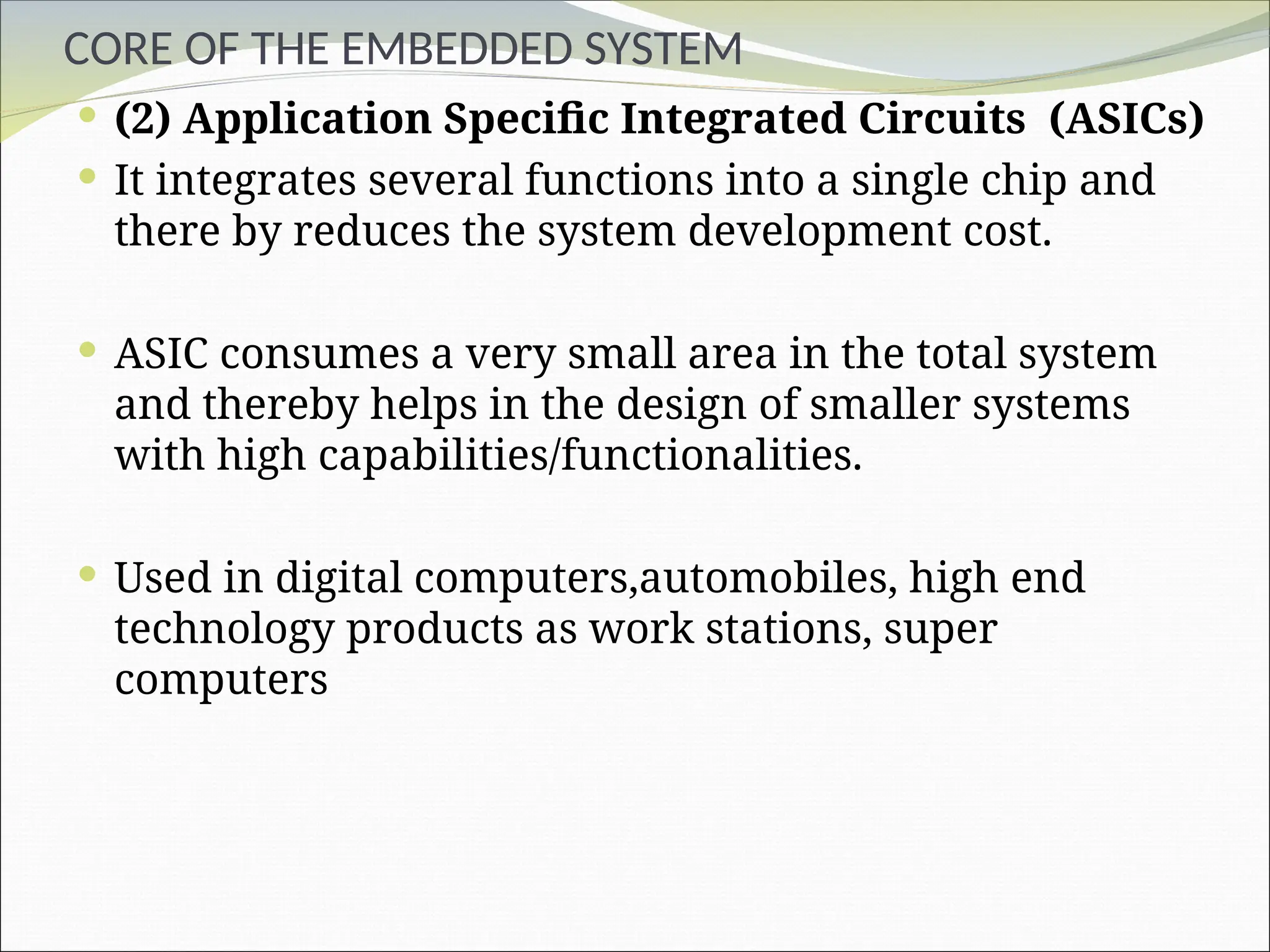
(2) Application Specific Integrated Circuits (ASICs)
It integrates several functions into a single chip and
there by reduces the system development cost.
ASIC consumes a very small area in the total system
and thereby helps in the design of smaller systems
with high capabilities/functionalities.
Used in digital computers,automobiles, high end
technology products as work stations, super
computers
55.
CORE OF THEEMBEDDED SYSTEM
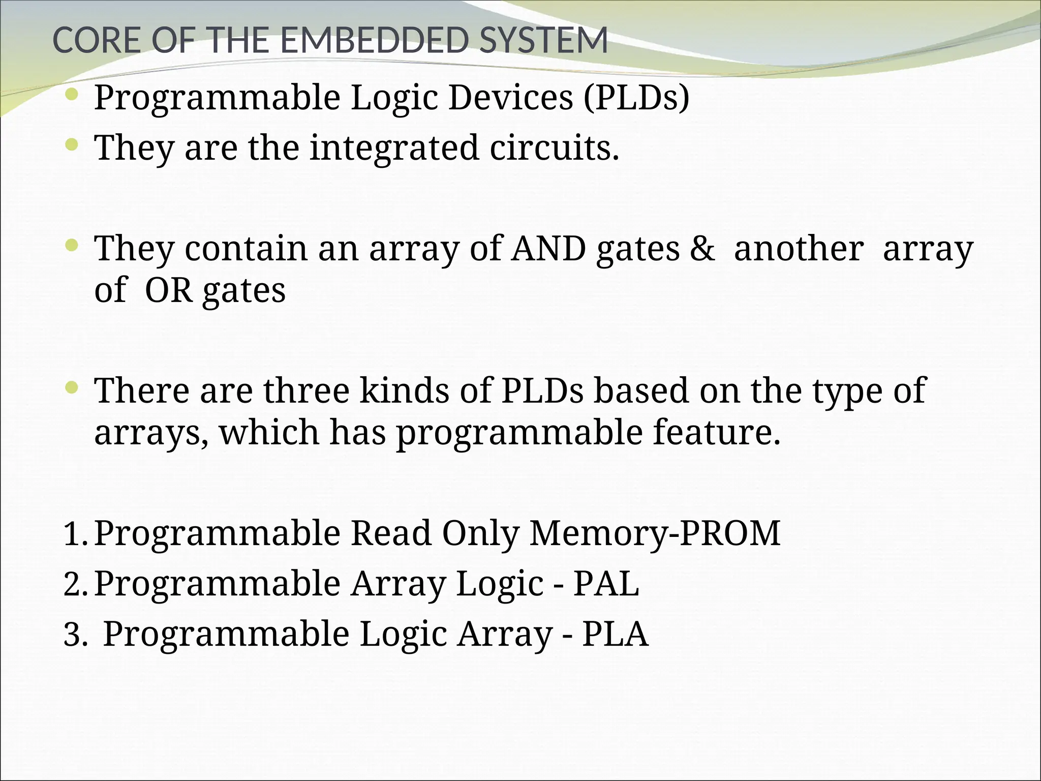
Programmable Logic Devices (PLDs)
They are the integrated circuits.
They contain an array of AND gates & another array
of OR gates
There are three kinds of PLDs based on the type of
arrays, which has programmable feature.
1.Programmable Read Only Memory-PROM
2.Programmable Array Logic - PAL
3. Programmable Logic Array - PLA
56.
CORE OF THEEMBEDDED SYSTEM
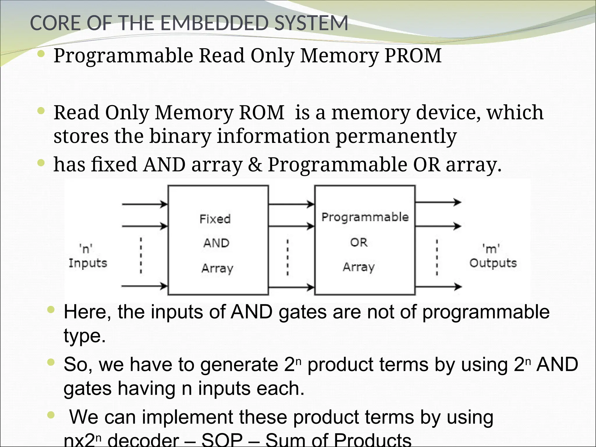
Programmable Read Only Memory PROM
Read Only Memory ROM is a memory device, which
stores the binary information permanently
has fixed AND array & Programmable OR array.
Here, the inputs of AND gates are not of programmable
type.
So, we have to generate 2n
product terms by using 2n
AND
gates having n inputs each.
We can implement these product terms by using
n
57.
CORE OF THEEMBEDDED SYSTEM
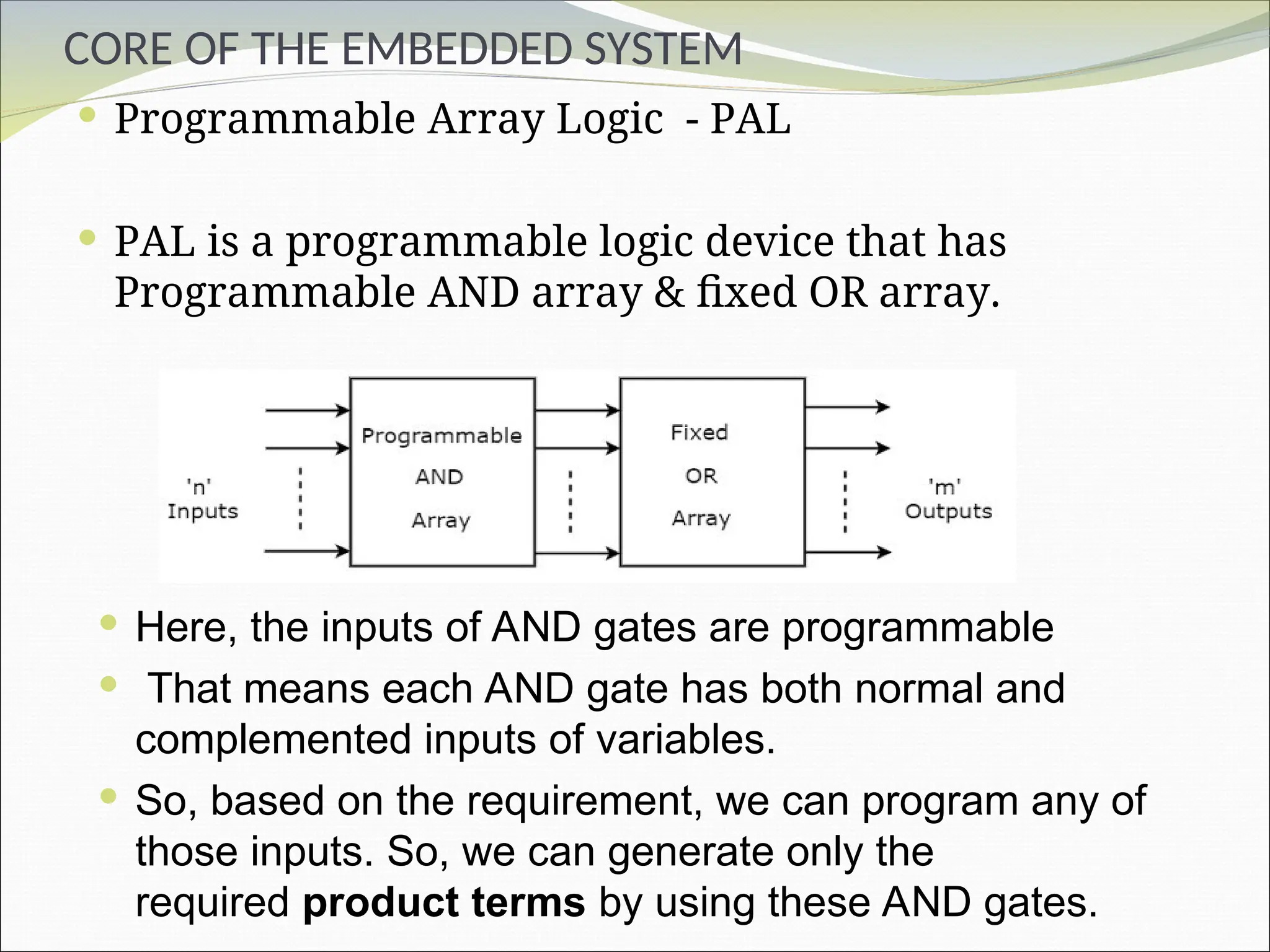
Programmable Array Logic - PAL
PAL is a programmable logic device that has
Programmable AND array & fixed OR array.
Here, the inputs of AND gates are programmable
That means each AND gate has both normal and
complemented inputs of variables.
So, based on the requirement, we can program any of
those inputs. So, we can generate only the
required product terms by using these AND gates.
58.
CORE OF THEEMBEDDED SYSTEM
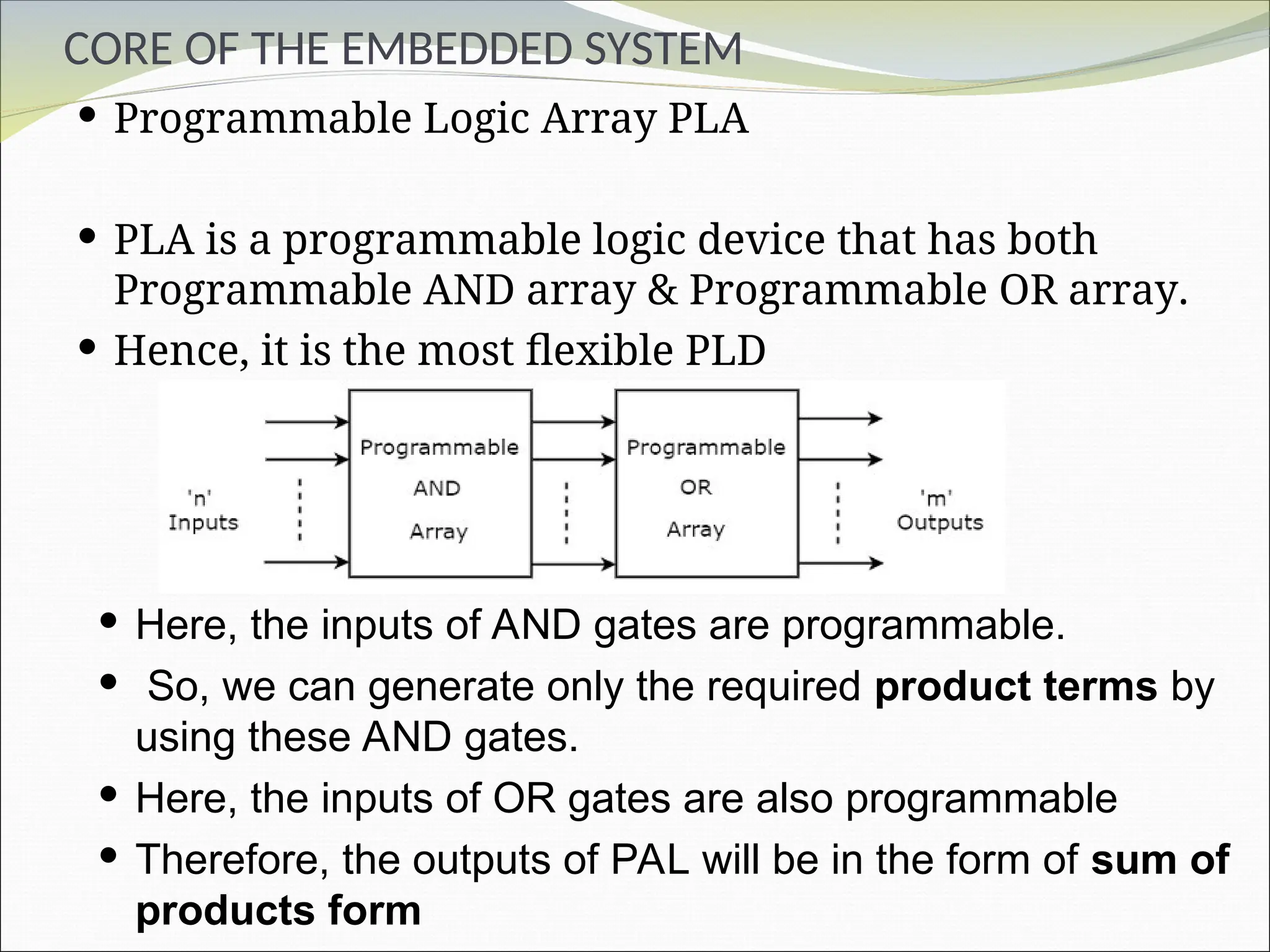
Programmable Logic Array PLA
PLA is a programmable logic device that has both
Programmable AND array & Programmable OR array.
Hence, it is the most flexible PLD
Here, the inputs of AND gates are programmable.
So, we can generate only the required product terms by
using these AND gates.
Here, the inputs of OR gates are also programmable
Therefore, the outputs of PAL will be in the form of sum of
products form
59.
CORE OF THEEMBEDDED SYSTEM
Commercial off-the-shelf Components (COTS)
A software and/or hardware product that is
commercially ready-made and available for sale, lease,
or license to the general public
A Commercial Off-the-Shelf ( COTS) product is one
which is used ‘as-is’
EX :
Toy car control units including the RF circuitry part,
high performance,
High frequency microwave electronics (2–200 ghz),
High bandwidth analog-to-digital converters,
Devices and components for operation at very high
temperatures,
Electro-optic IR imaging arrays, UV/IR detectors, etc
60.
CORE OF THEEMBEDDED SYSTEM
Commercial off-the-shelf Components (COTS)
EX :
The Microsoft Office.
Microsoft Office Suite.
Adobe Photoshop.
Windows 10 Operating System.
61.
MEMORY
MEMORY
Memoryis an important part of a processor/controller
based embedded systems.
Some of the processors/controllers contain built in
memory and this memory is referred as on-chip
memory.
Others do not contain any memory inside the chip and
requires external memory to be connected with the
controller/processor to store the control algorithm.
It is called off-chip memory.
62.
MEMORY
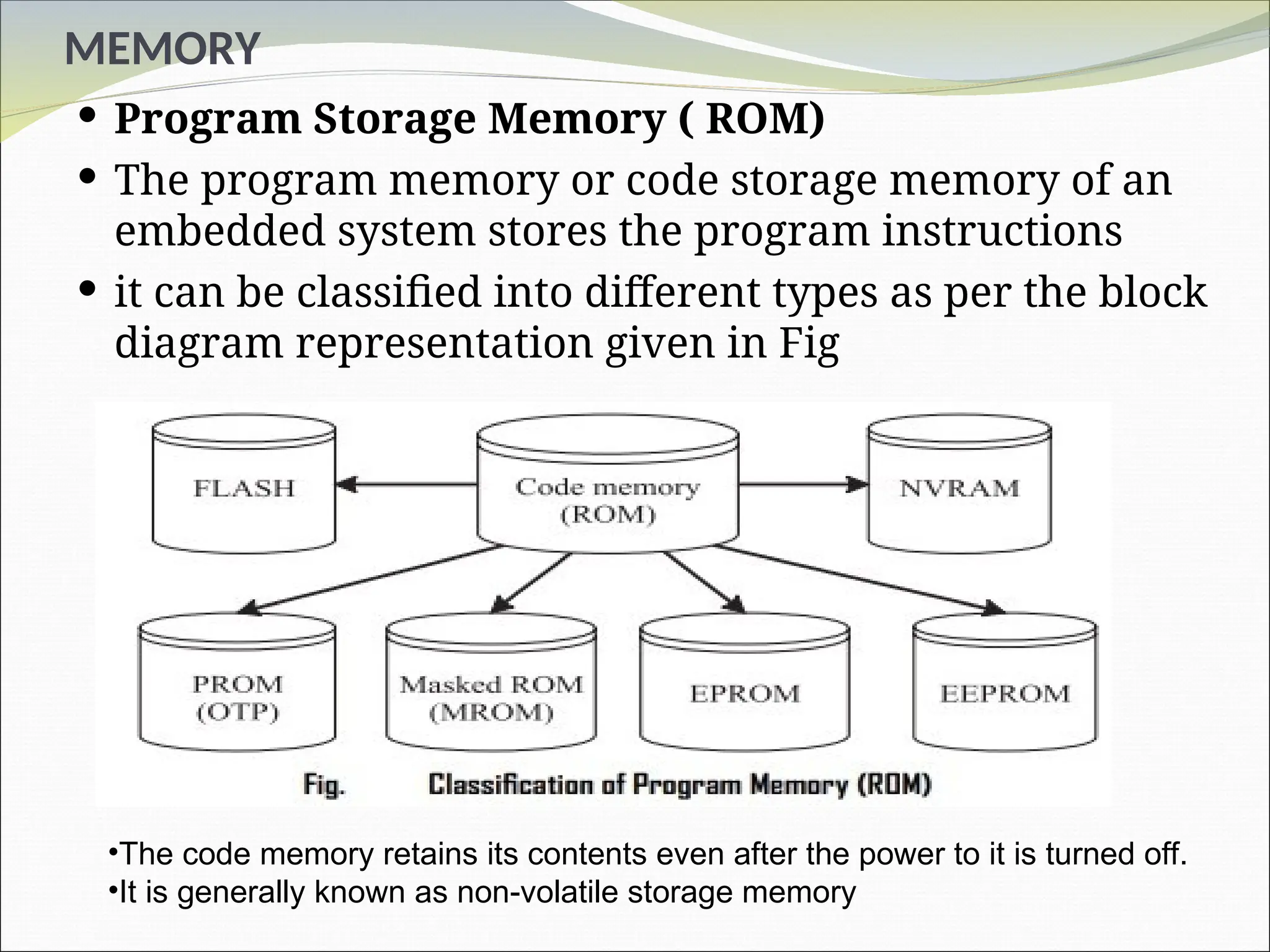
Program StorageMemory ( ROM)
The program memory or code storage memory of an
embedded system stores the program instructions
it can be classified into different types as per the block
diagram representation given in Fig
•The code memory retains its contents even after the power to it is turned off.
•It is generally known as non-volatile storage memory
63.
MEMORY
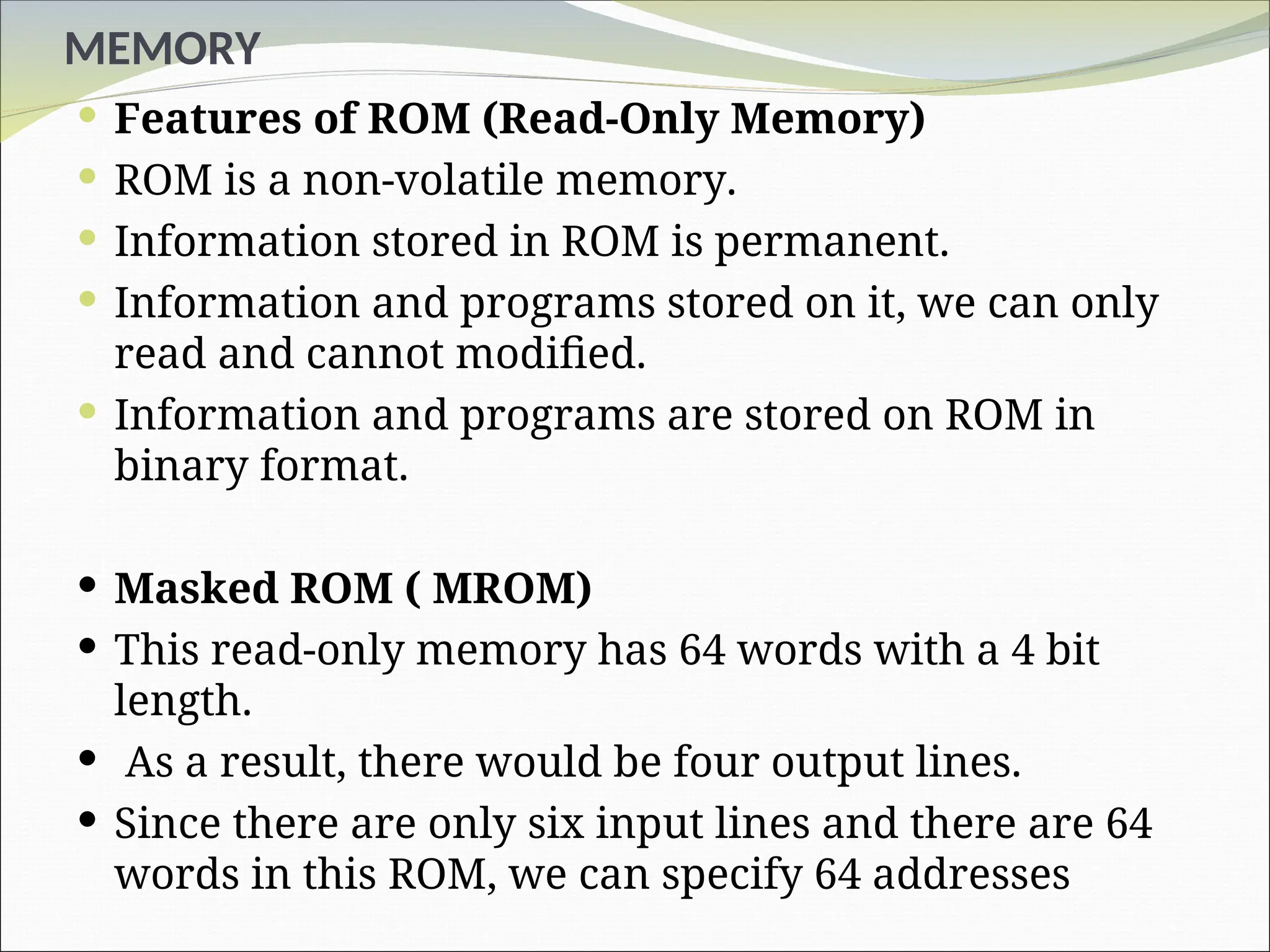
Features ofROM (Read-Only Memory)
ROM is a non-volatile memory.
Information stored in ROM is permanent.
Information and programs stored on it, we can only
read and cannot modified.
Information and programs are stored on ROM in
binary format.
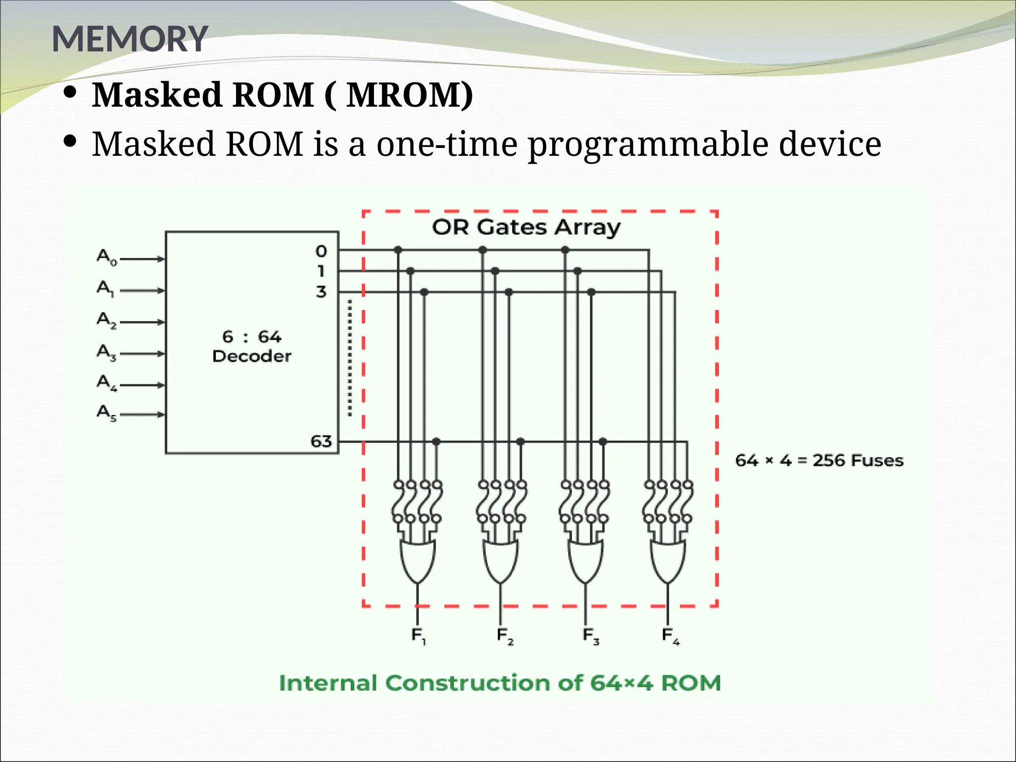
Masked ROM ( MROM)
This read-only memory has 64 words with a 4 bit
length.
As a result, there would be four output lines.
Since there are only six input lines and there are 64
words in this ROM, we can specify 64 addresses
MEMORY
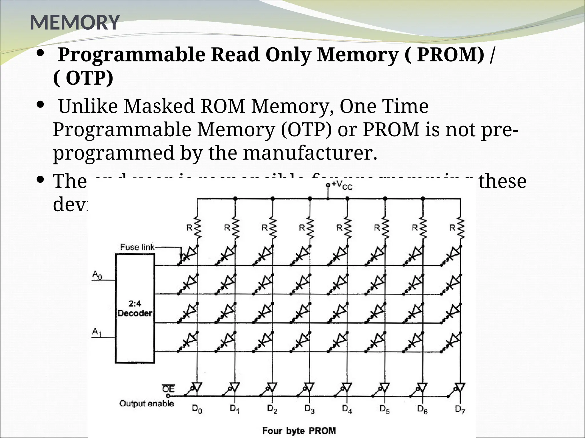
Programmable ReadOnly Memory ( PROM) /
( OTP)
Unlike Masked ROM Memory, One Time
Programmable Memory (OTP) or PROM is not pre-
programmed by the manufacturer.
The end user is responsible for programming these
devices
66.
MEMORY
Programmable ReadOnly Memory ( PROM) /
( OTP)
polysilicon wires arranged in a matrix
Programmer which selectively burns the fuses
according to the bit pattern to be stored.
Fuses which are not blown/notburned represents a
logic “1” whereas fuses which are blown/burned
represents a logic “0
OTPs cannot be reprogrammed.
67.
MEMORY
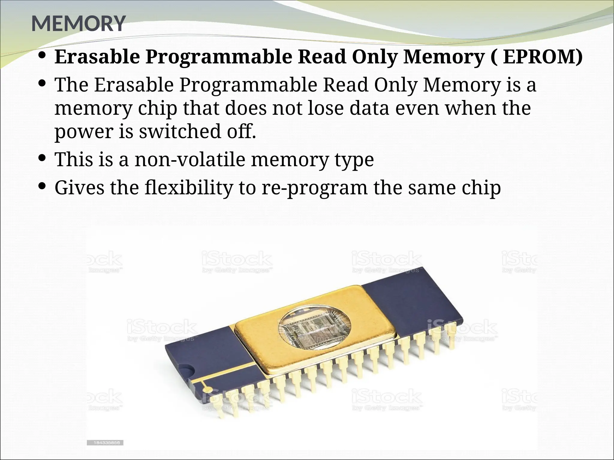
Erasable ProgrammableRead Only Memory ( EPROM)
The Erasable Programmable Read Only Memory is a
memory chip that does not lose data even when the
power is switched off.
This is a non-volatile memory type
Gives the flexibility to re-program the same chip
68.
MEMORY
Erasable ProgrammableRead Only Memory ( EPROM)
Each EPROM is individually programmed by an
electronic device. (FET)
After that, the data can be erased by exposing the EPROM
to strong ultraviolet light.
An EPROM contains a transparent fused quartz window
at the top of the package which allows exposure to
ultraviolet light
It takes 20 to 30 minutes to erase it. Time consuming
69.
MEMORY
Electrically ErasableProgrammable Read Only
Memory ( EEPROM)
EEPROM can be erased and programmed electrically.
Most EEPROM chips have a life span of 10,000 to
100,000 write cycles, which is considerably greater
than the write cycles of EPROM chips.
An individual byte of data can erase and
reprogrammed entirety, not selectively by the
electrical voltage.
70.
MEMORY
FLASH MEMORY
Flash memory is a non-volatile memory chip used for
storage and for transfering data between a personal
computer (PC) and digital devices.
It has the ability to be electronically reprogrammed
and erased. (EEPROM)
It is often found in USB flash drives, MP3 players,
digital cameras and solid-state drives.
71.
MEMORY
How DoesFlash Memory Work?
1.Current flows through the transistor between each
cell’s source (electric input) and drain (electric output).
2.The transistor controls the current’s path of by acting
as an on-off switch, or a gate.
3.An “on” transistor allows the flow of electrons across
the cell, which stores a 1 in binary code.
4.An “off” transistor blocks electrons and stores a 0.
72.
MEMORY
NVRAM
Itis an acronym for Non-Volatile Random Access
Memory. NVRAM is a type of Random Access Memory
(RAM) that retains its information when power is
turned off.
The NVRAM is a small 24 pin DIP (Dual Inline
Package) integrated circuit chip and is thus able to
obtain the power needed to keep it running from the
CMOS battery installed in your motherboard.
Stores information like serial number, Ethernet MAC
(Media Access Control) address, HOSTID, date of
manufactur
73.
MEMORY
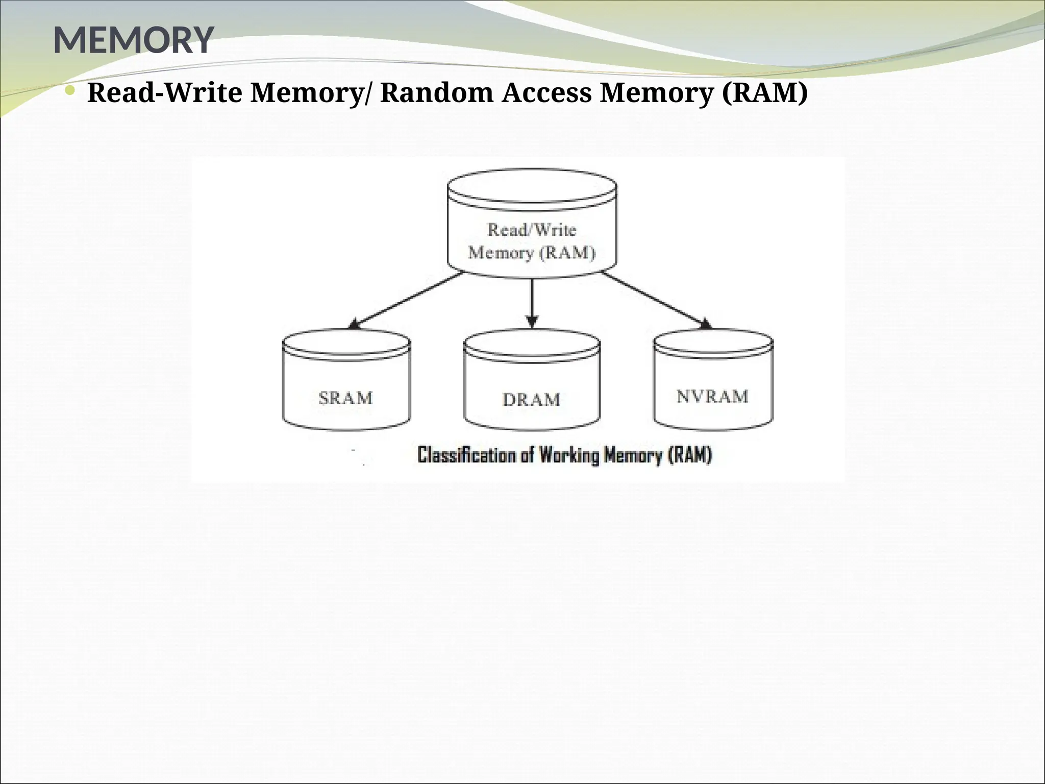
Read-Write Memory/Random Access Memory
(RAM)
RAM is the data memory or working memory of the
controller/processor.
Controller/processor can read from it and write to it.
It is also called read-write memory or the main
memory or the primary memory.
The programs and data that the CPU requires during
the execution of a program are stored in this memory.
74.
MEMORY
Read-Write Memory/Random Access Memory
(RAM)
RAM is volatile, meaning when the power is turned
off, all the contents are destroyed.
RAM is a direct access memory, meaning we can
access the desired memory location directly without
the need for traversing through the entire memory
locations to reach the desired memory position (i.e.
random access of memory location)
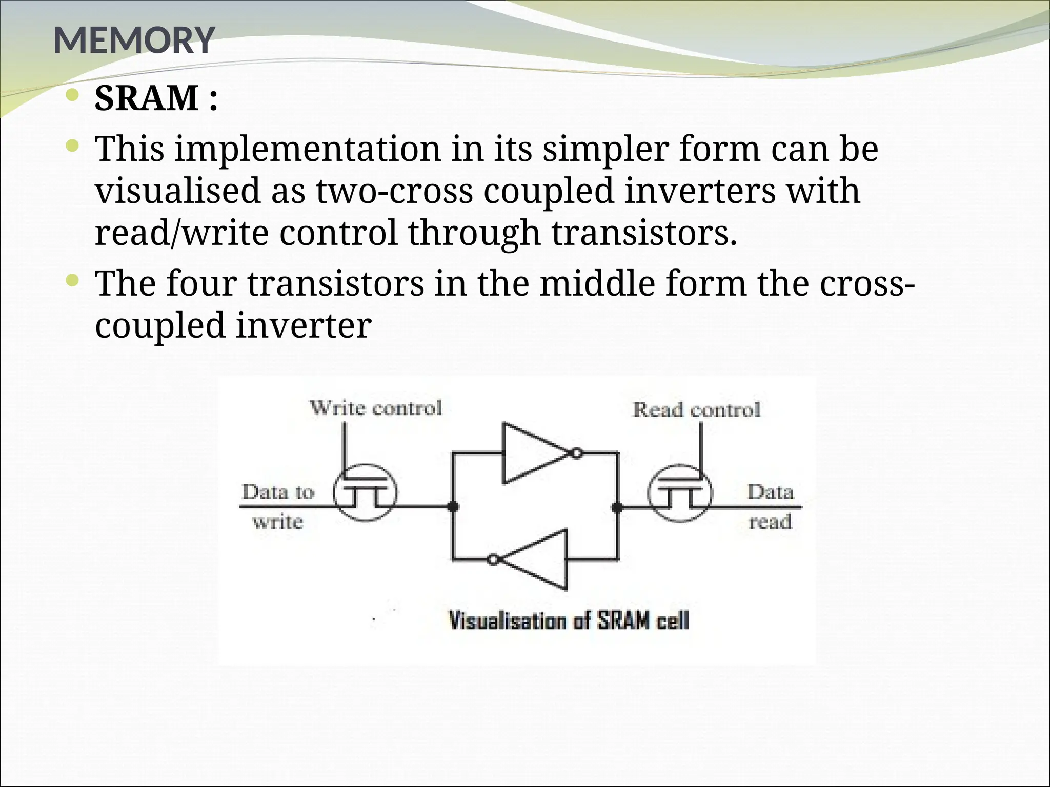
MEMORY
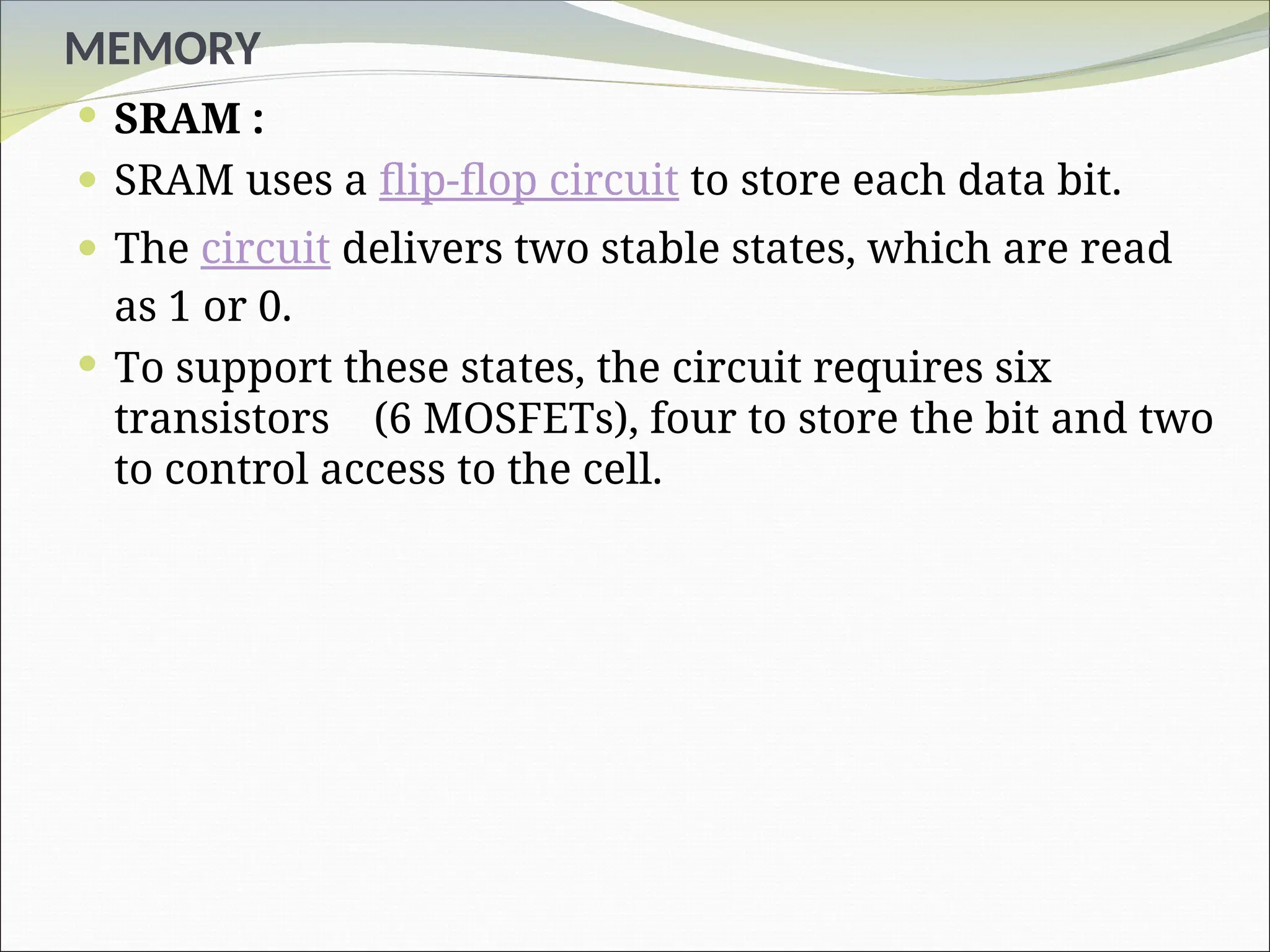
SRAM :
SRAM uses a flip-flop circuit to store each data bit.
The circuit delivers two stable states, which are read
as 1 or 0.
To support these states, the circuit requires six
transistors (6 MOSFETs), four to store the bit and two
to control access to the cell.
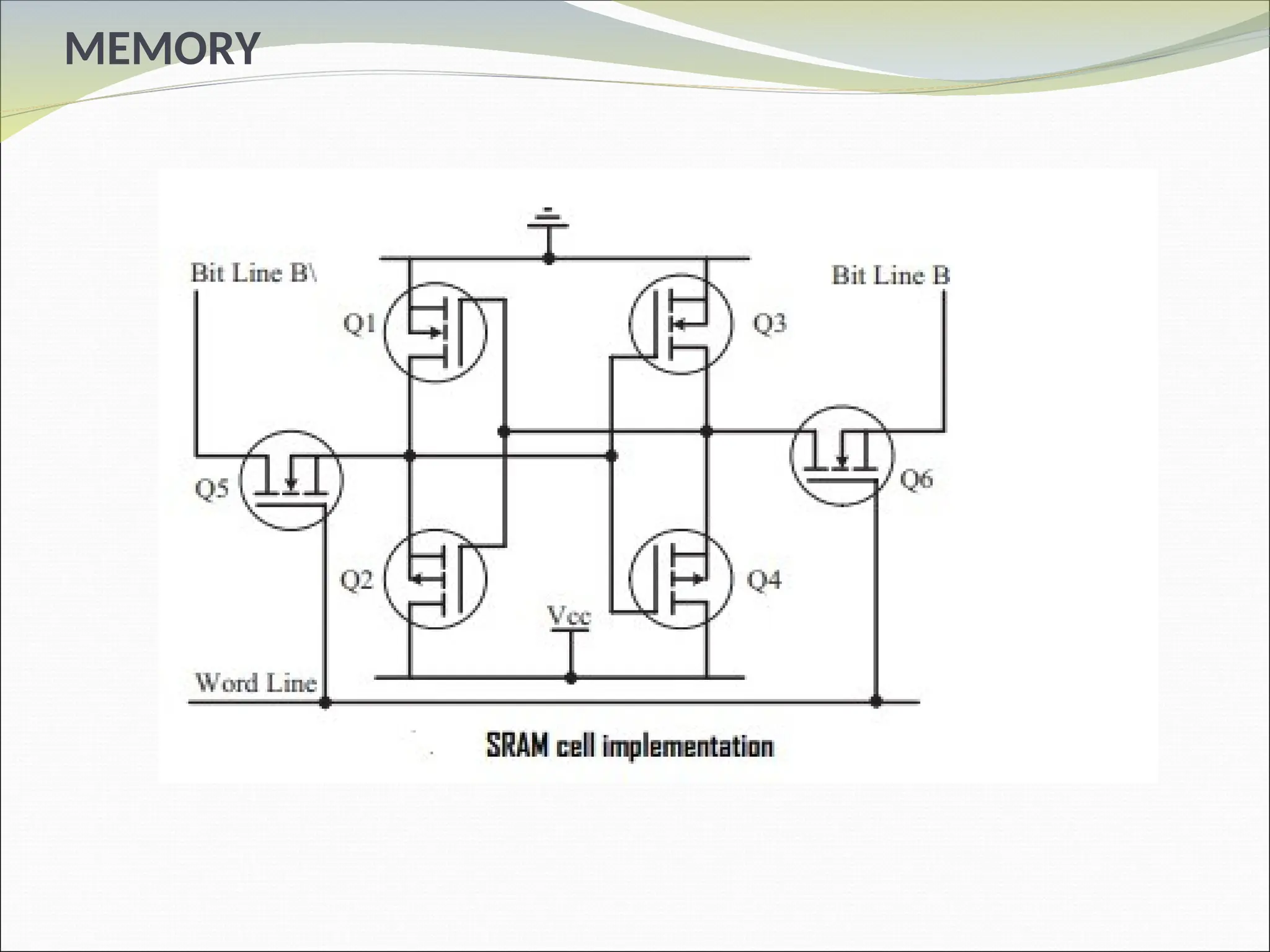
MEMORY
SRAM :
This implementation in its simpler form can be
visualised as two-cross coupled inverters with
read/write control through transistors.
The four transistors in the middle form the cross-
coupled inverter
79.
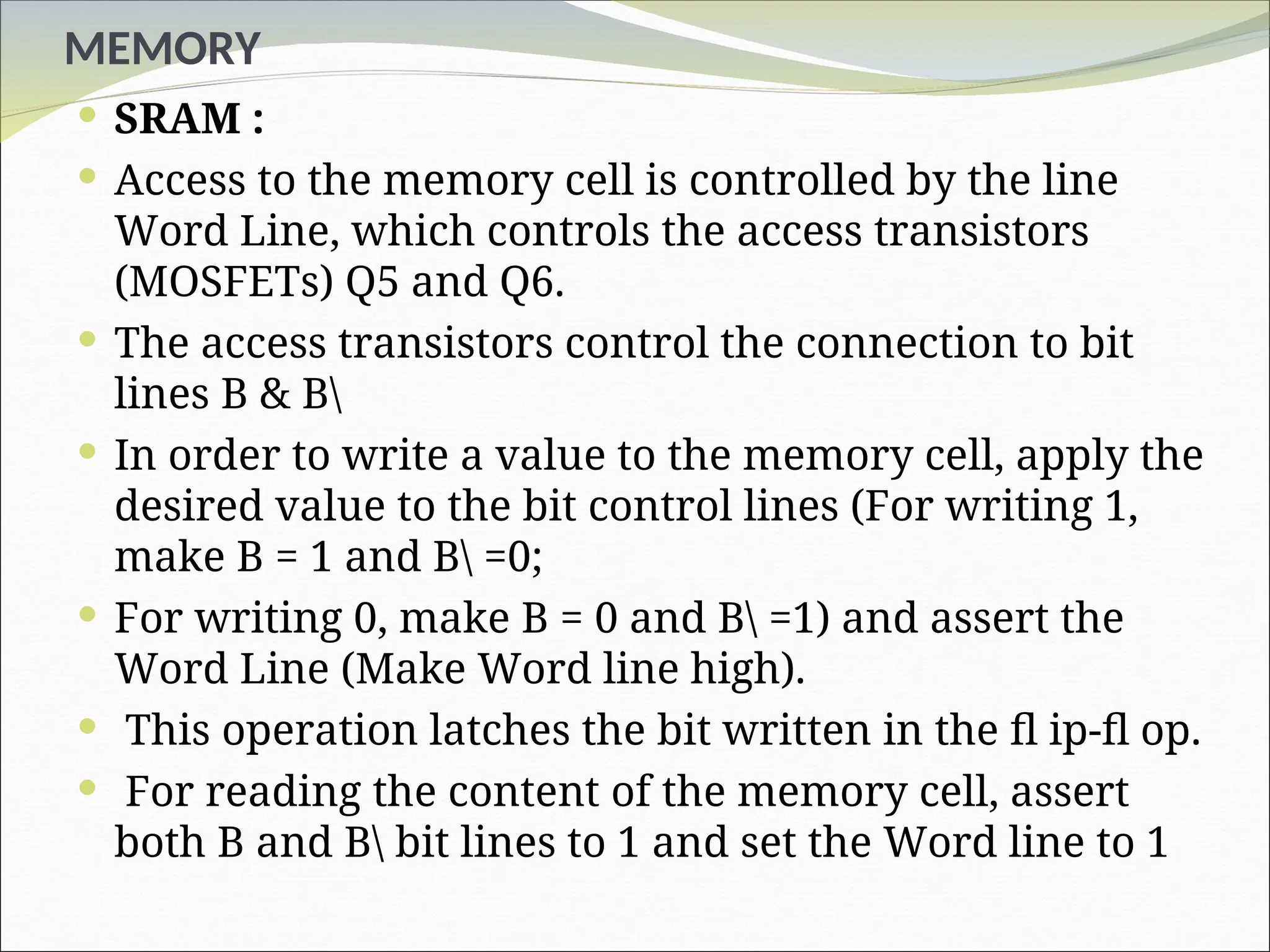
MEMORY
SRAM :
Access to the memory cell is controlled by the line
Word Line, which controls the access transistors
(MOSFETs) Q5 and Q6.
The access transistors control the connection to bit
lines B & B
In order to write a value to the memory cell, apply the
desired value to the bit control lines (For writing 1,
make B = 1 and B =0;
For writing 0, make B = 0 and B =1) and assert the
Word Line (Make Word line high).
This operation latches the bit written in the fl ip-fl op.
For reading the content of the memory cell, assert
both B and B bit lines to 1 and set the Word line to 1
80.
MEMORY
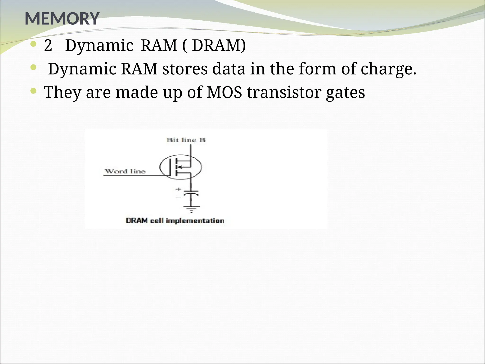
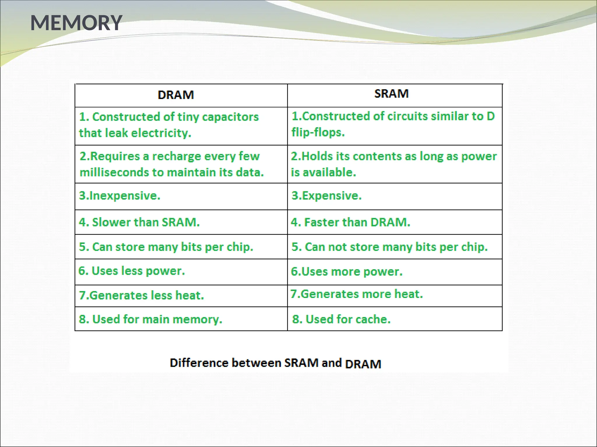
2 DynamicRAM ( DRAM)
Dynamic RAM stores data in the form of charge.
They are made up of MOS transistor gates
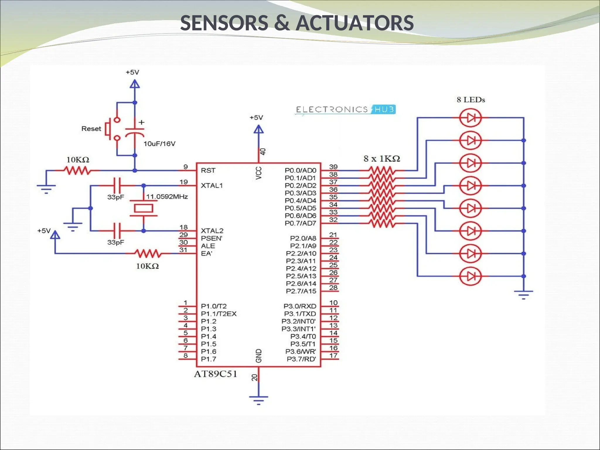
SENSORS & ACTUATORS
Sensors
Asensor is a transducer device that converts
energy from one form to another for any
measurement or control purpose
Ex : The sensor used in some of the smart watch devices
to measure the light intensity is an Ambient Light
Sensor (ALS)
Actuators
Actuator is a form of transducer device
(mechanical or electrical) which converts signals to
corresponding physical action (motion)
Ex :
83.
SENSORS & ACTUATORS
TheI/O Subsystem
The I/O subsystem of the embedded system
facilitates the interaction of the embedded system
with the external world
The interaction happens through the sensors and
actuators connected to the input and output ports
respectively of the embedded system.
The sensors may not be directly interfaced to the
input ports, instead they may be interfaced through
signal conditioning and translating systems like ADC,
optocouplers ..etc.
84.
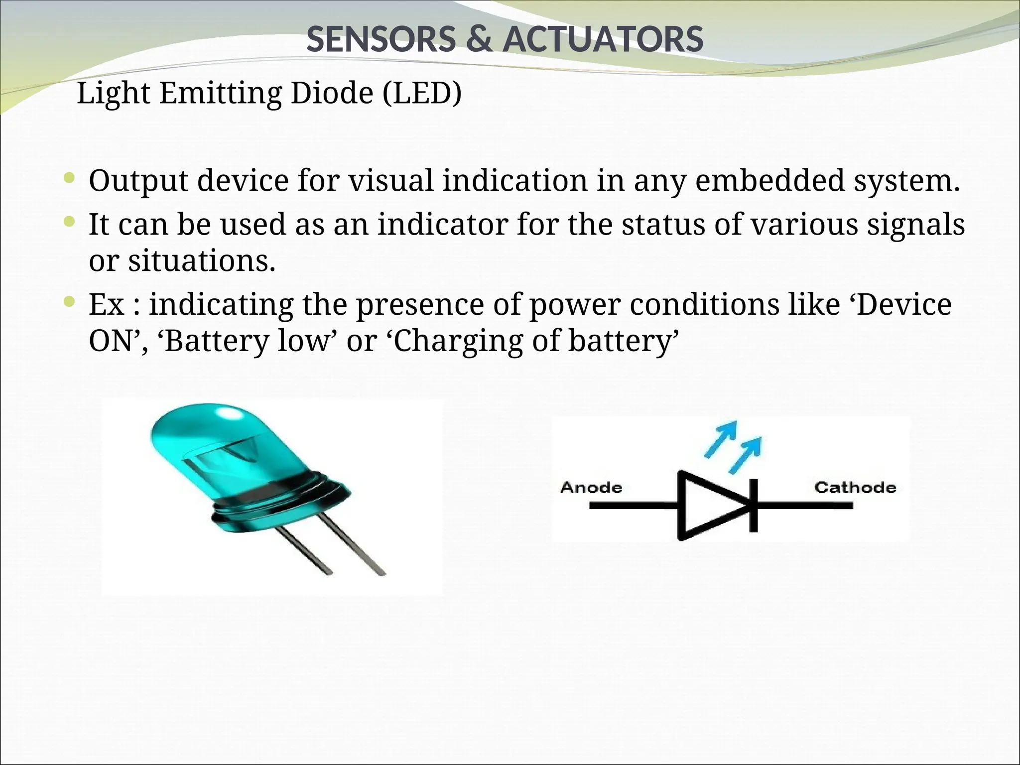
SENSORS & ACTUATORS
LightEmitting Diode (LED)
Output device for visual indication in any embedded system.
It can be used as an indicator for the status of various signals
or situations.
Ex : indicating the presence of power conditions like ‘Device
ON’, ‘Battery low’ or ‘Charging of battery’
85.
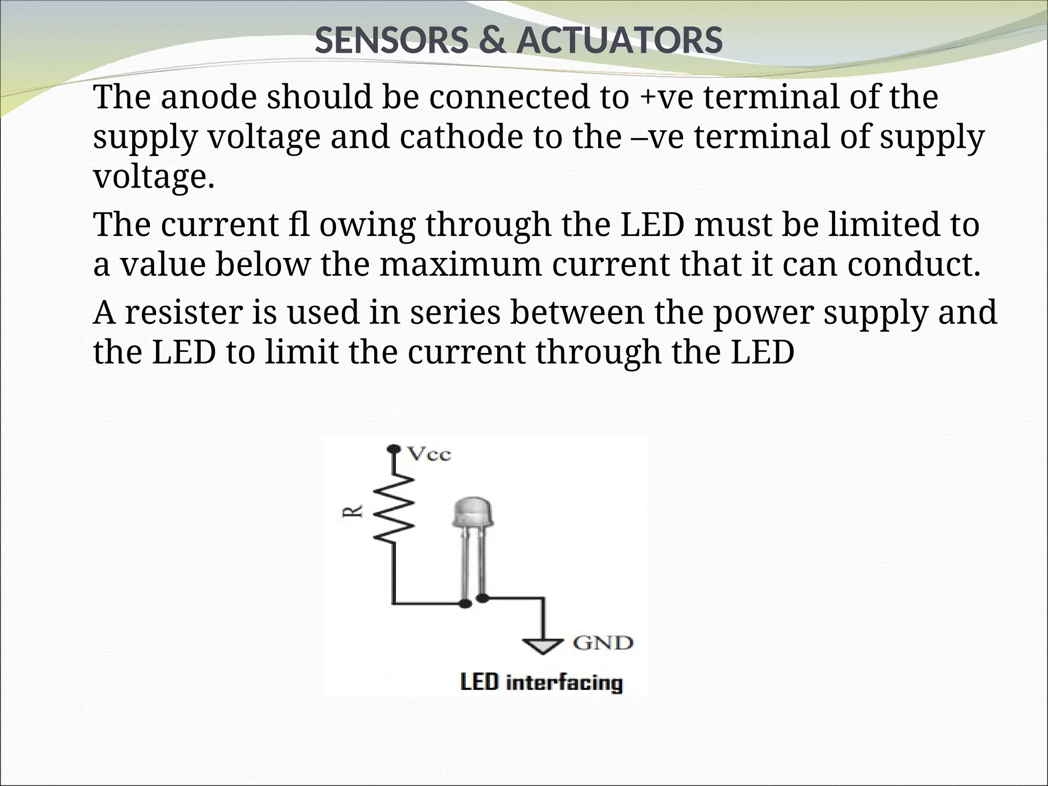
SENSORS & ACTUATORS
Theanode should be connected to +ve terminal of the
supply voltage and cathode to the –ve terminal of supply
voltage.
The current fl owing through the LED must be limited to
a value below the maximum current that it can conduct.
A resister is used in series between the power supply and
the LED to limit the current through the LED
SENSORS & ACTUATORS
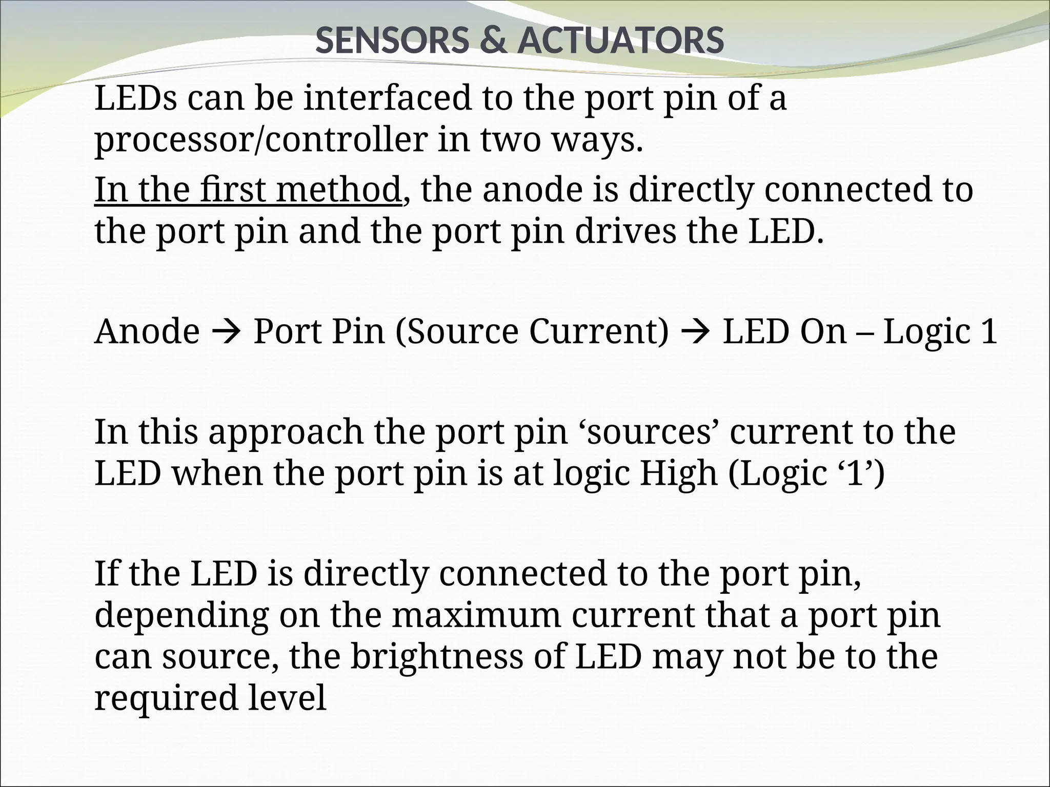
LEDscan be interfaced to the port pin of a
processor/controller in two ways.
In the first method, the anode is directly connected to
the port pin and the port pin drives the LED.
Anode Port Pin (Source Current) LED On – Logic 1
In this approach the port pin ‘sources’ current to the
LED when the port pin is at logic High (Logic ‘1’)
If the LED is directly connected to the port pin,
depending on the maximum current that a port pin
can source, the brightness of LED may not be to the
required level
88.
SENSORS & ACTUATORS
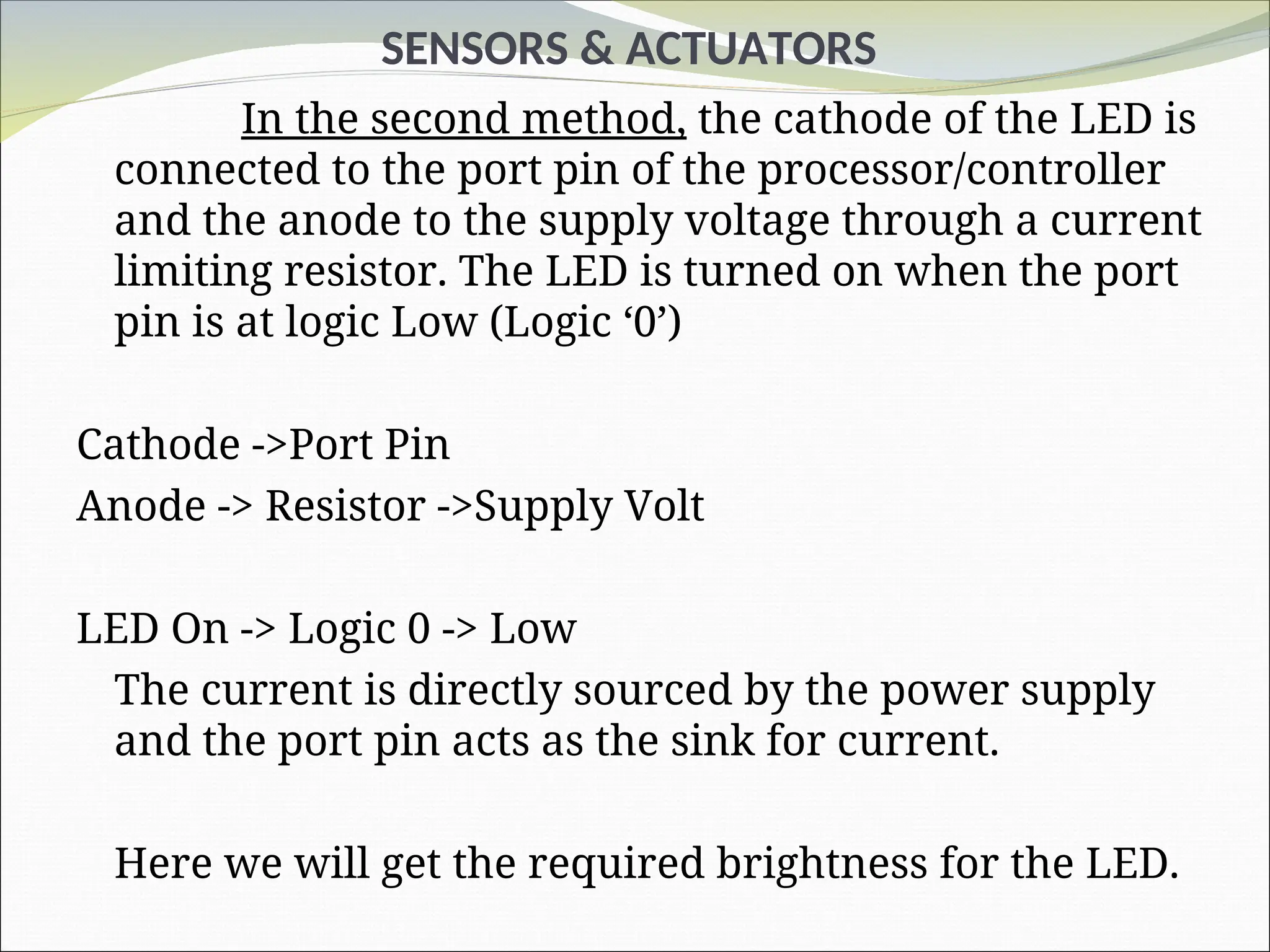
Inthe second method, the cathode of the LED is
connected to the port pin of the processor/controller
and the anode to the supply voltage through a current
limiting resistor. The LED is turned on when the port
pin is at logic Low (Logic ‘0’)
Cathode ->Port Pin
Anode -> Resistor ->Supply Volt
LED On -> Logic 0 -> Low
The current is directly sourced by the power supply
and the port pin acts as the sink for current.
Here we will get the required brightness for the LED.
89.
SENSORS & ACTUATORS
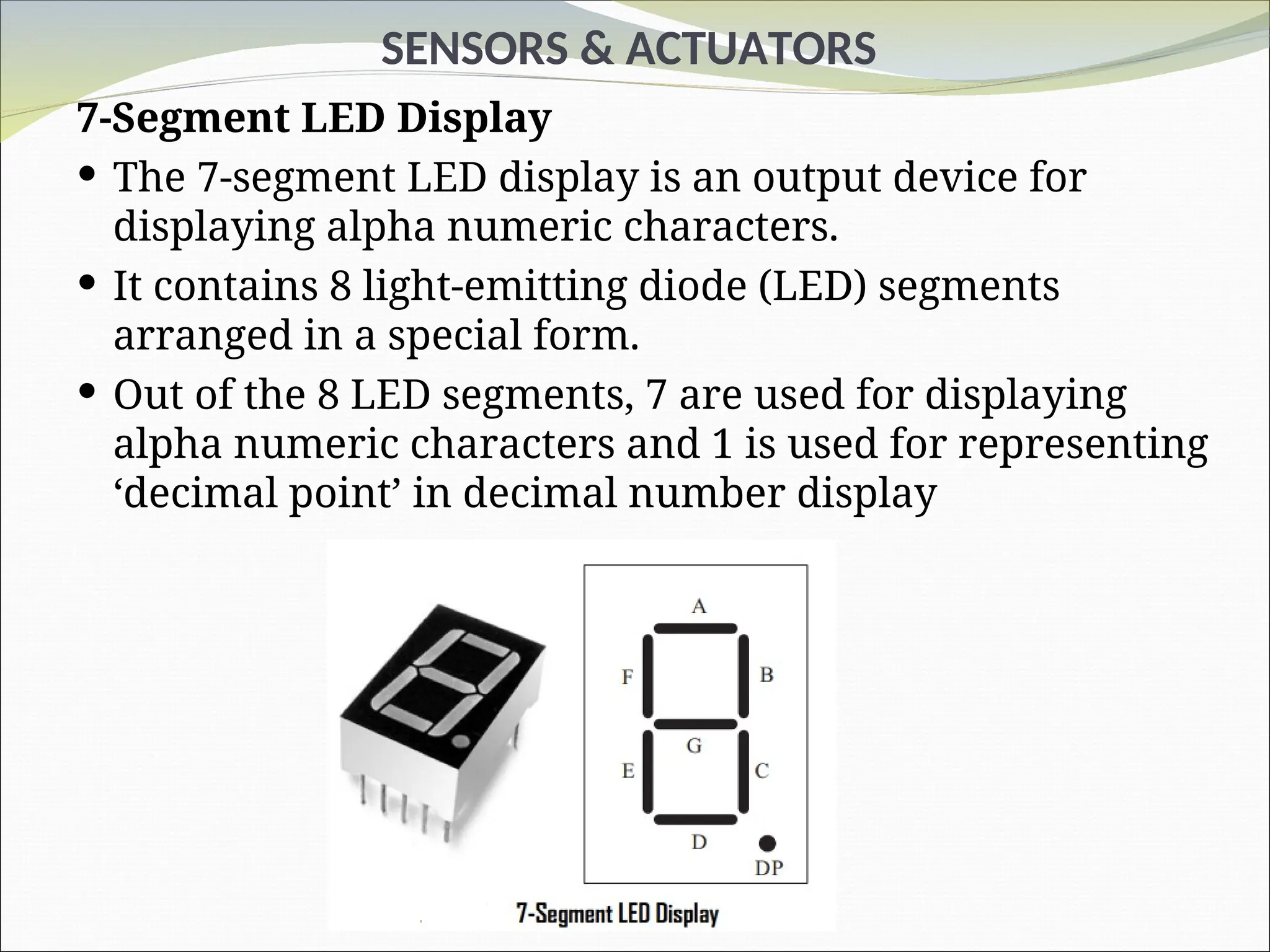
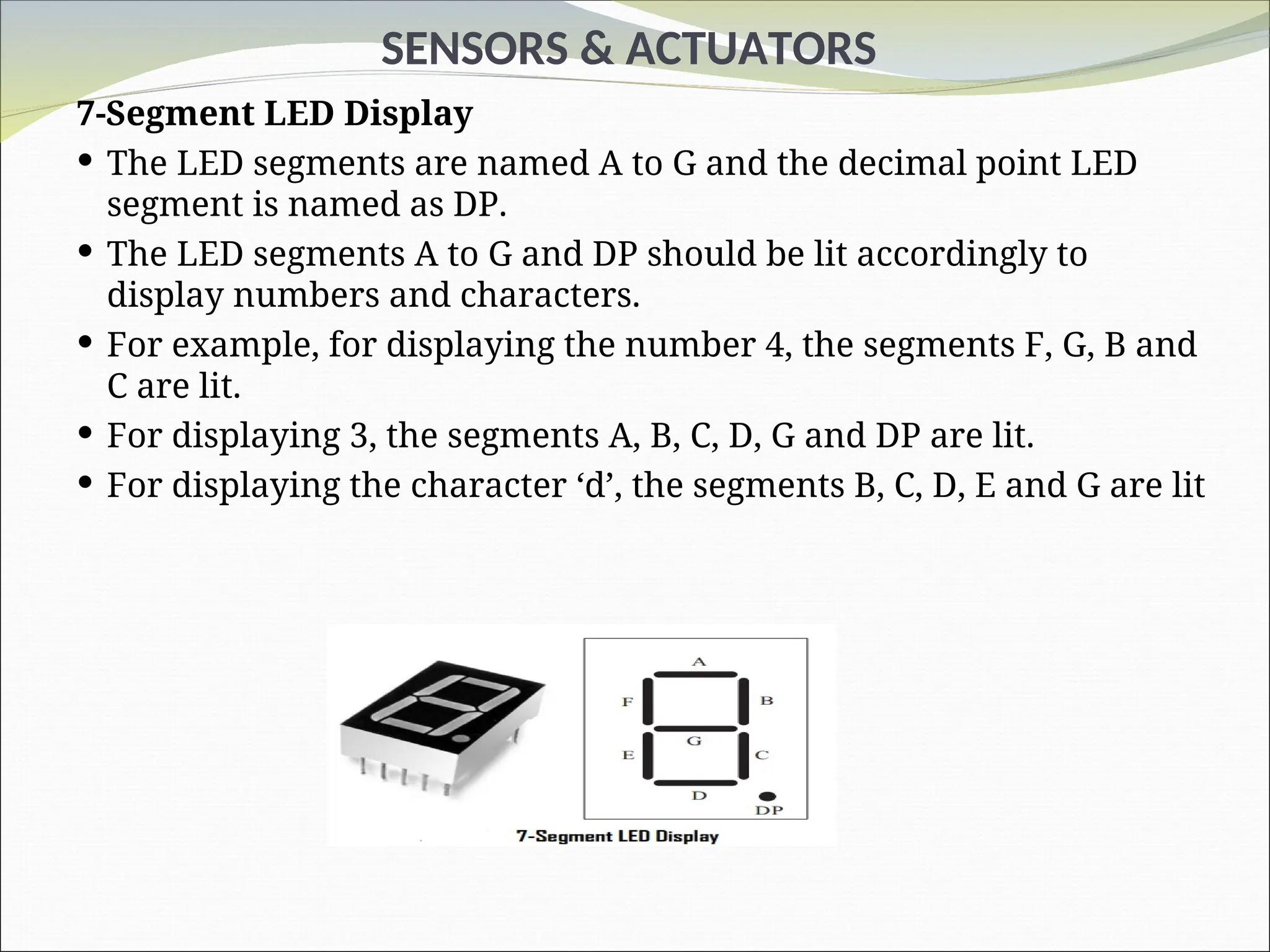
7-SegmentLED Display
The 7-segment LED display is an output device for
displaying alpha numeric characters.
It contains 8 light-emitting diode (LED) segments
arranged in a special form.
Out of the 8 LED segments, 7 are used for displaying
alpha numeric characters and 1 is used for representing
‘decimal point’ in decimal number display
90.
SENSORS & ACTUATORS
7-SegmentLED Display
The LED segments are named A to G and the decimal point LED
segment is named as DP.
The LED segments A to G and DP should be lit accordingly to
display numbers and characters.
For example, for displaying the number 4, the segments F, G, B and
C are lit.
For displaying 3, the segments A, B, C, D, G and DP are lit.
For displaying the character ‘d’, the segments B, C, D, E and G are lit
91.
SENSORS & ACTUATORS
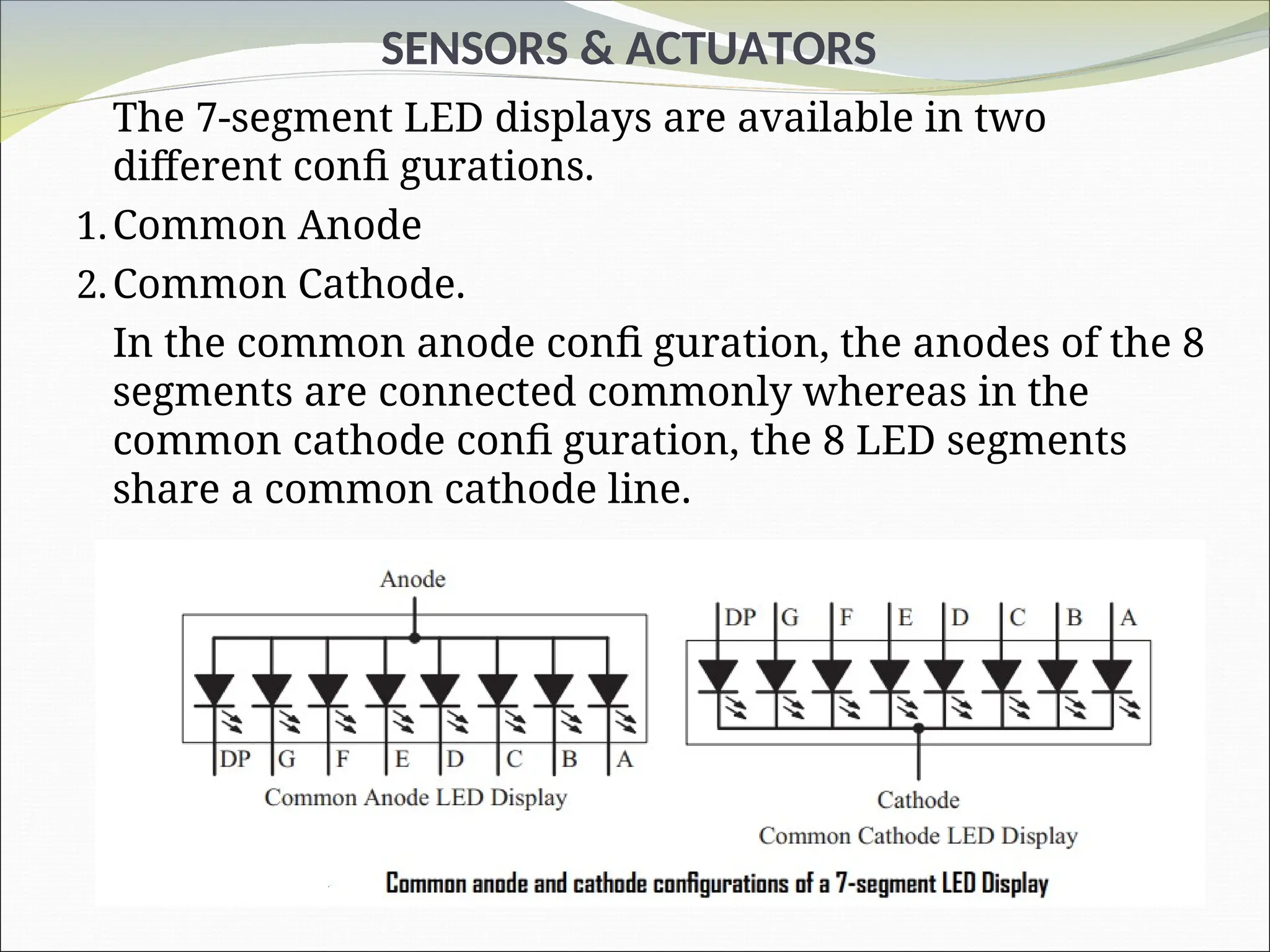
The7-segment LED displays are available in two
different confi gurations.
1.Common Anode
2.Common Cathode.
In the common anode confi guration, the anodes of the 8
segments are connected commonly whereas in the
common cathode confi guration, the 8 LED segments
share a common cathode line.
92.
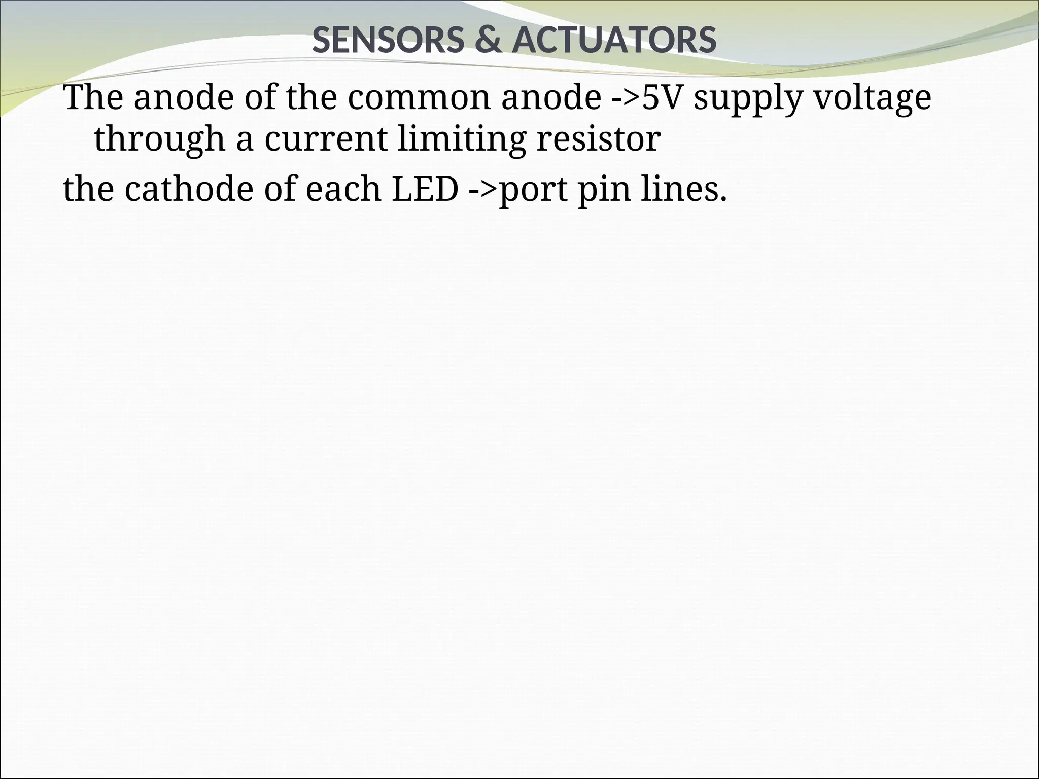
SENSORS & ACTUATORS
Theanode of the common anode ->5V supply voltage
through a current limiting resistor
the cathode of each LED ->port pin lines.
93.
SENSORS & ACTUATORS
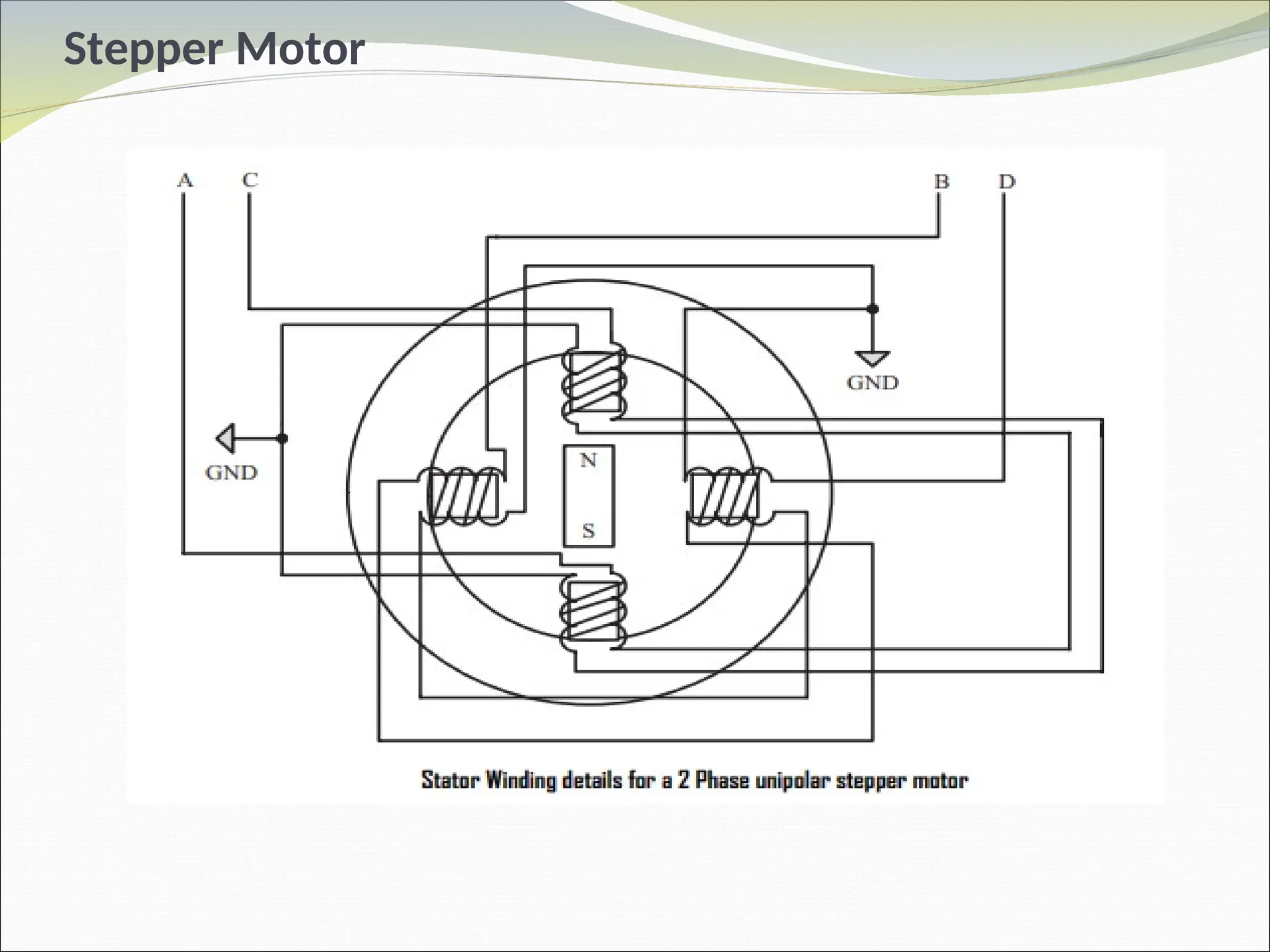
StepperMotor
A stepper motor is an electro-mechanical device
which generates discrete displacement (motion) in
response to dc electrical signals.
The dc motor produces continuous rotation on
applying dc voltage whereas a stepper motor
produces discrete rotation in response to the dc
voltage applied to it.
Stepper motors are widely used in industrial
embedded applications, consumer electronic products
and robotics control systems.
The paper feed mechanism of a printer/fax makes use
of stepper motors for its functioning
94.
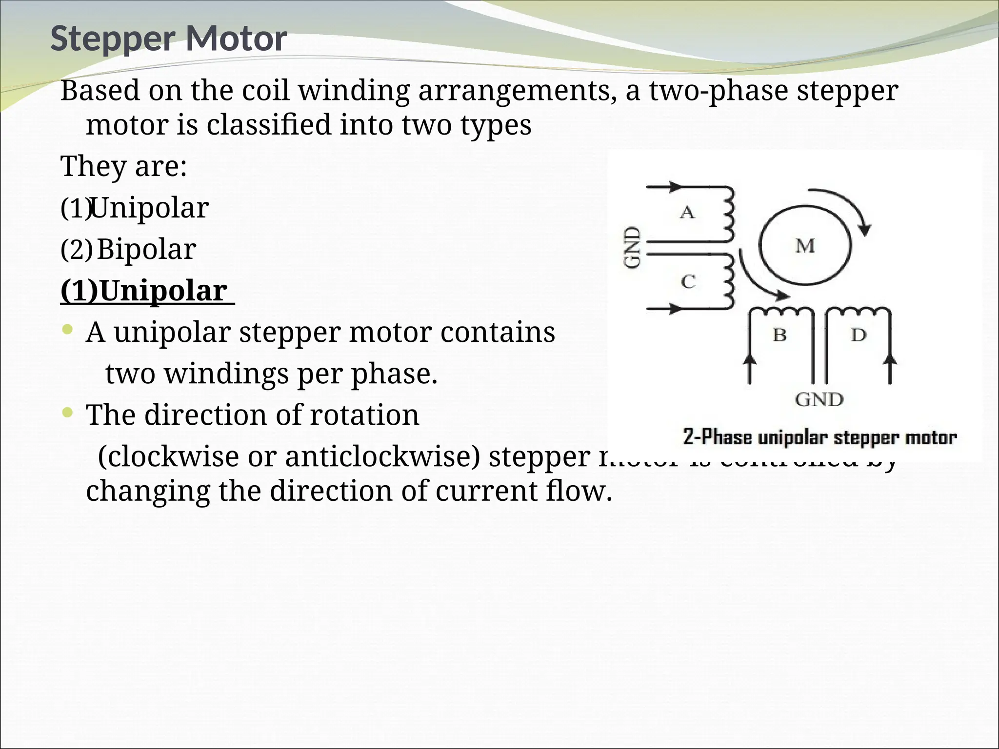
Stepper Motor
Based onthe coil winding arrangements, a two-phase stepper
motor is classified into two types
They are:
(1)Unipolar
(2)Bipolar
(1)Unipolar
A unipolar stepper motor contains
two windings per phase.
The direction of rotation
(clockwise or anticlockwise) stepper motor is controlled by
changing the direction of current flow.
95.
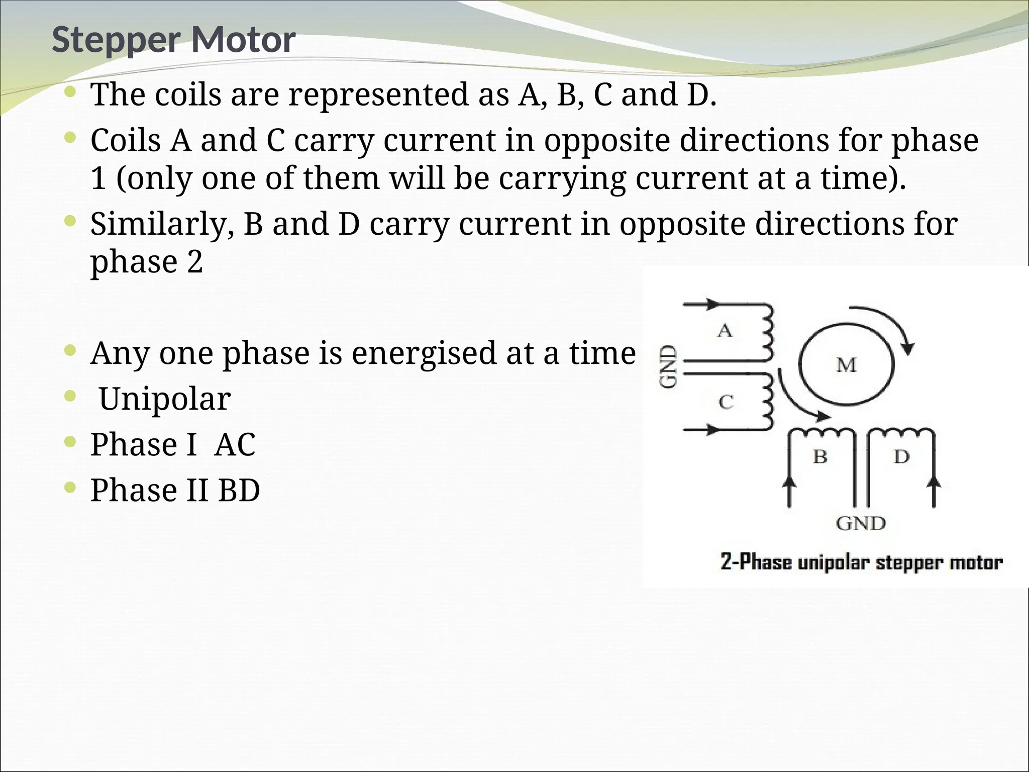
Stepper Motor
Thecoils are represented as A, B, C and D.
Coils A and C carry current in opposite directions for phase
1 (only one of them will be carrying current at a time).
Similarly, B and D carry current in opposite directions for
phase 2
Any one phase is energised at a time
Unipolar
Phase I AC
Phase II BD
96.
Stepper Motor
(2)Bipolar
A bipolar stepper motor contains single winding per phase
For reversing the motor rotation the current flow through the windings is
reversed dynamically.
It requires complex circuitry for current flow reversal
The stepping of stepper motor can be implemented in different ways by changing
the sequence of activation of the stator windings
97.
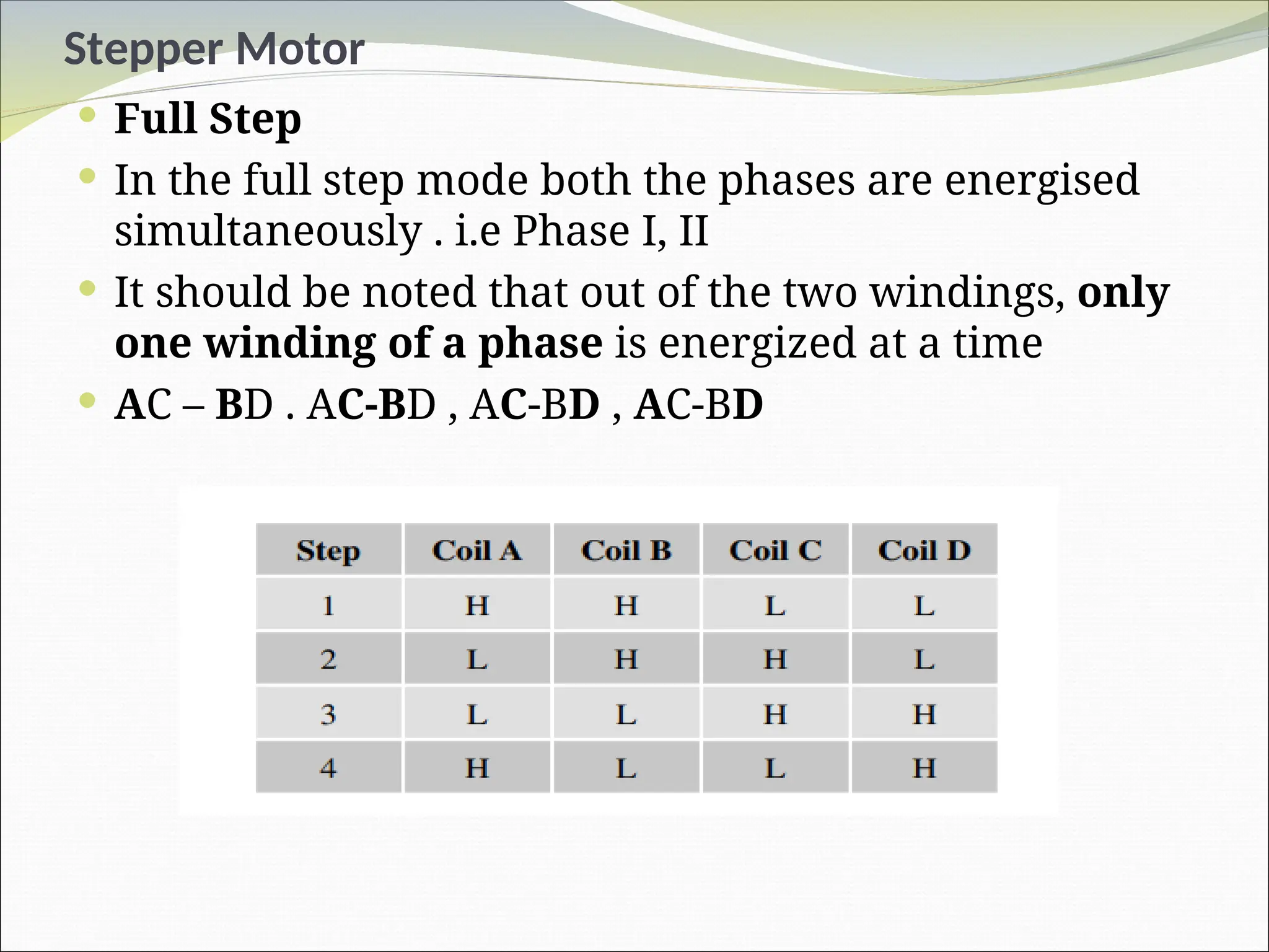
Stepper Motor
FullStep
In the full step mode both the phases are energised
simultaneously . i.e Phase I, II
It should be noted that out of the two windings, only
one winding of a phase is energized at a time
AC – BD . AC-BD , AC-BD , AC-BD
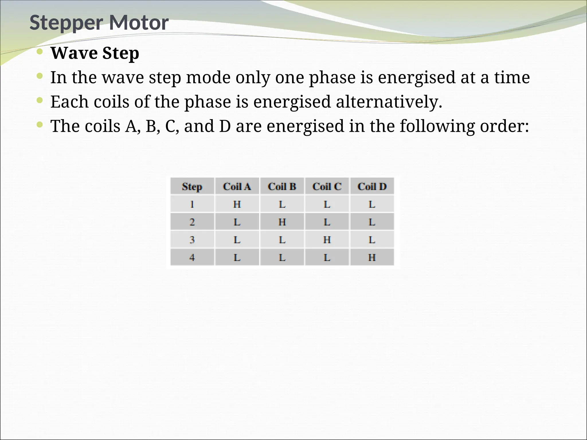
Stepper Motor
WaveStep
In the wave step mode only one phase is energised at a time
Each coils of the phase is energised alternatively.
The coils A, B, C, and D are energised in the following order:
100.
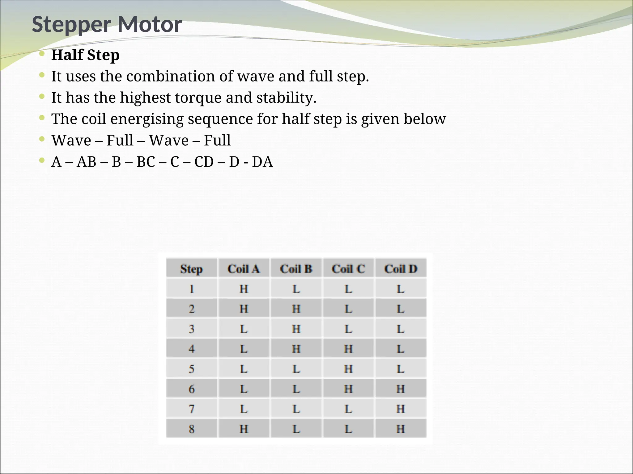
Stepper Motor
HalfStep
It uses the combination of wave and full step.
It has the highest torque and stability.
The coil energising sequence for half step is given below
Wave – Full – Wave – Full
A – AB – B – BC – C – CD – D - DA
101.
Stepper Motor
Thecurrent requirement for stepper motor is little
high and hence the port pins of a
microcontroller/processor may not be able to drive
them directly.
Also the supply voltage required to operate stepper
motor varies normally in the range 5V to 24 V.
Depending on the current and voltage requirements,
special driving circuits are required to interface the
stepper motor with microcontroller/processors
102.
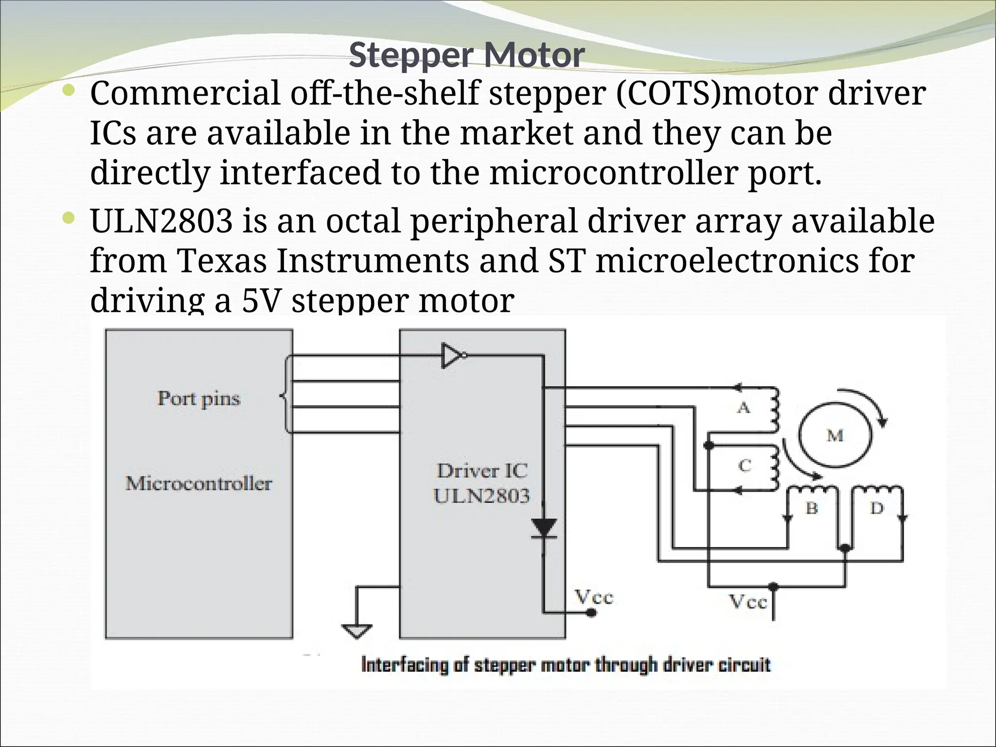
Stepper Motor
Commercialoff-the-shelf stepper (COTS)motor driver
ICs are available in the market and they can be
directly interfaced to the microcontroller port.
ULN2803 is an octal peripheral driver array available
from Texas Instruments and ST microelectronics for
driving a 5V stepper motor
103.
Relay
Relay
Actsas a switching device
Relay is an electro-mechanical device.
In embedded application, the ‘Relay’ unit acts as
dynamic path selectors for signals and power
The ‘Relay’ unit contains a relay coil made up of
insulated wire on a metal core and a metal armature
with one or more contacts.
104.
Relay
Relay
‘Relay’works on electromagnetic principle.
When a voltage is applied to the relay coil, current fl
ows through the coil, which in turn generates a
magnetic fi eld.
The magnetic fi eld attracts the armature core and
moves the contact point
105.
Relay
Relay
Themovement of the contact point changes the
power/signal fl ow path.
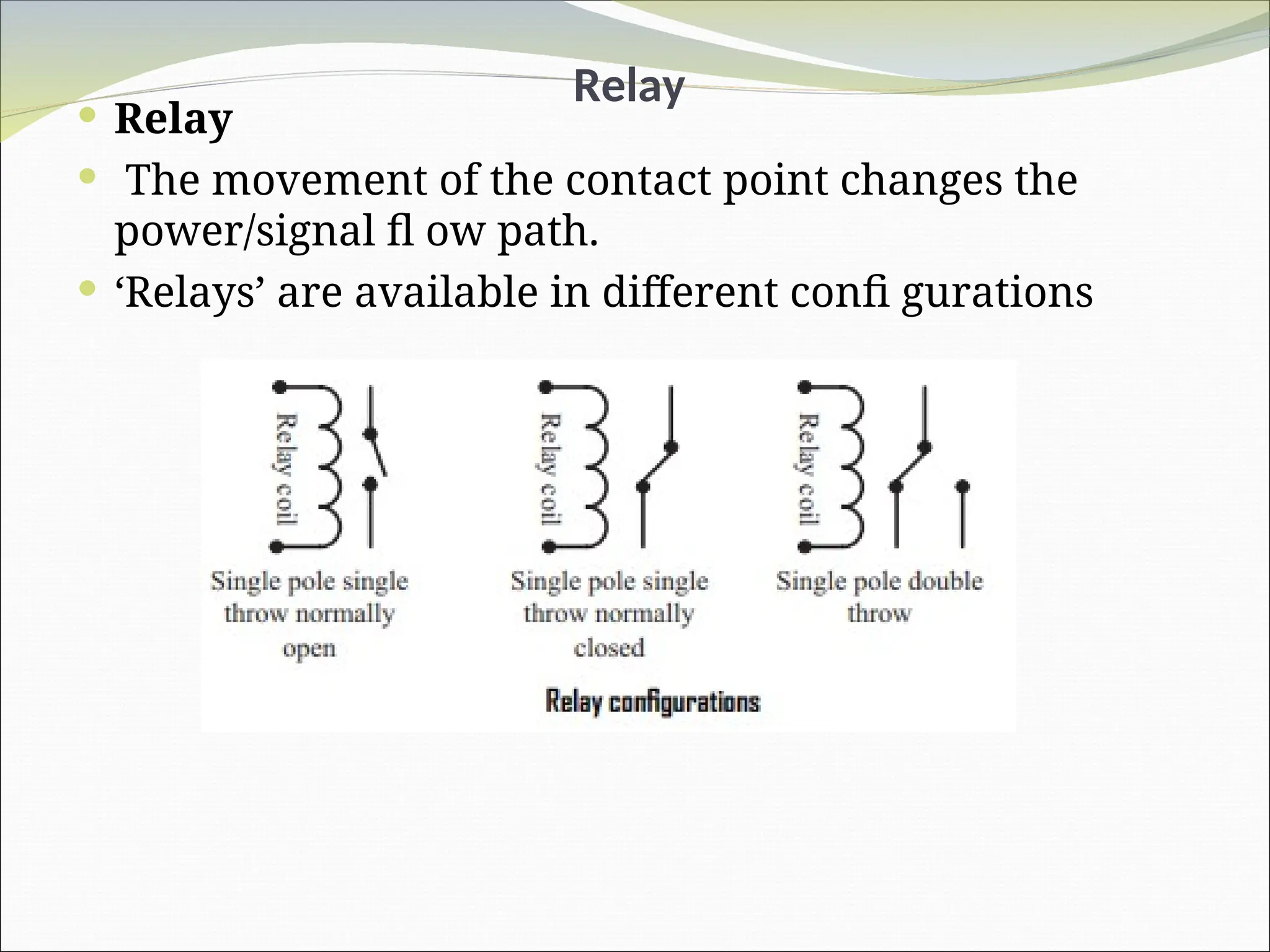
‘Relays’ are available in different confi gurations
106.
Relay
Relay
TheSingle Pole Single Throw confi guration has only
one path for information fl ow.
The path is either open or closed in normal condition.
For normally Open Single Pole Single Throw relay, the
circuit is normally open and it becomes closed when
the relay is energised.
For normally closed Single Pole Single Throw confi
guration, the circuit is normally closed and it becomes
open when the relay is energised.
For Single Pole Double Throw Relay, there are two
paths for information fl ow and they are selected by
energising or de-energising the relay.
107.
Piezo Buzzer
PiezoBuzzer
Piezo buzzer is a piezoelectric device for generating
audio indications in embedded application.
A piezoelectric buzzer contains a piezoelectric
diaphragm which produces audible sound in response
to the voltage applied to it.
Piezoelectric buzzers are available in two types.
‘Self-driving’ and ‘External driving’.
108.
Piezo Buzzer
PiezoBuzzer
The ‘Self-driving’ circuit contains all the necessary
components to generate sound at a predefined tone.
It will generate a tone on applying the voltage.
External driving piezo buzzers supports the
generation of different tones.
The tone can be varied by applying a variable pulse
train to the piezoelectric buzzer
109.
Push Button Switch
Push Button Switch
It is an input device.
Push button switch comes in two confi gurations,
namely ‘Push to Make’ and ‘Push to Break’.
In the ‘Push to Make’ confi guration, the switch is
normally in the open state and it makes a circuit
contact when it is pushed or pressed.
In the ‘Push to Break’ confi guration, the switch is
normally in the closed state and it breaks the circuit
contact when it is pushed or pressed.
110.
Push Button Switch
Push Button Switch
The push button stays in the ‘closed’ (For Push to
Make type) or ‘open’ (For Push to Break type) state as
long as it is kept in the pushed state and it
breaks/makes the circuit connection when it is
released
The Push button is normally connected to the port pin
of the host processor/controller
Depending on the way in which the push button
interfaced to the controller, it can generate either a
‘HIGH’ pulse or a ‘LOW’ pulse
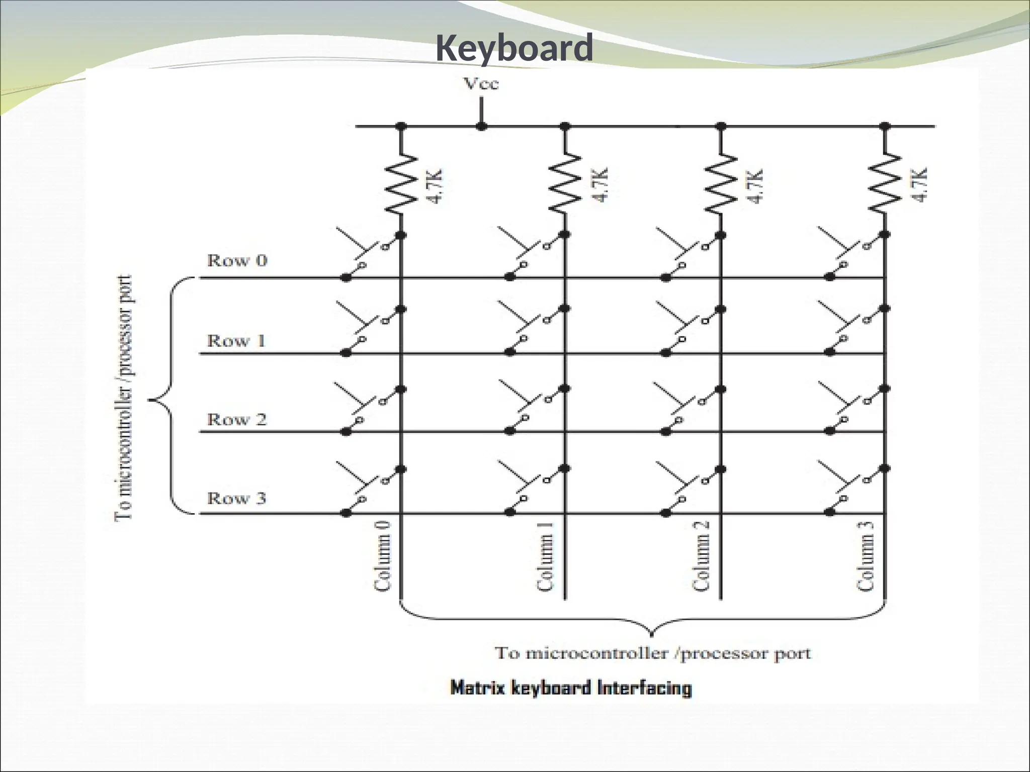
Keyboard
Keyboard
Keyboardis an input device for user interfacing.
If the number of keys required is very limited, push
button switches can be used and they can be directly
interfaced to the port pins for reading.
However, there may be situations demanding a large
number of keys for user input
In such situations it may not be possible to interface
each keys to a port pin due to the limitation in the
number of general purpose port pins available for the
processor/ controller
113.
Keyboard
Keyboard
Matrixkeyboard is an optimum solution for handling
large key requirements.
It greatly reduces the number of interface
connections.
For example, for interfacing 16 keys, in the direct
interfacing technique 16 port pins are required,
whereas in the matrix keyboard only 8 lines are
required.
The 16 keys are arranged in a 4 column × 4 Row
matrix
Keyboard
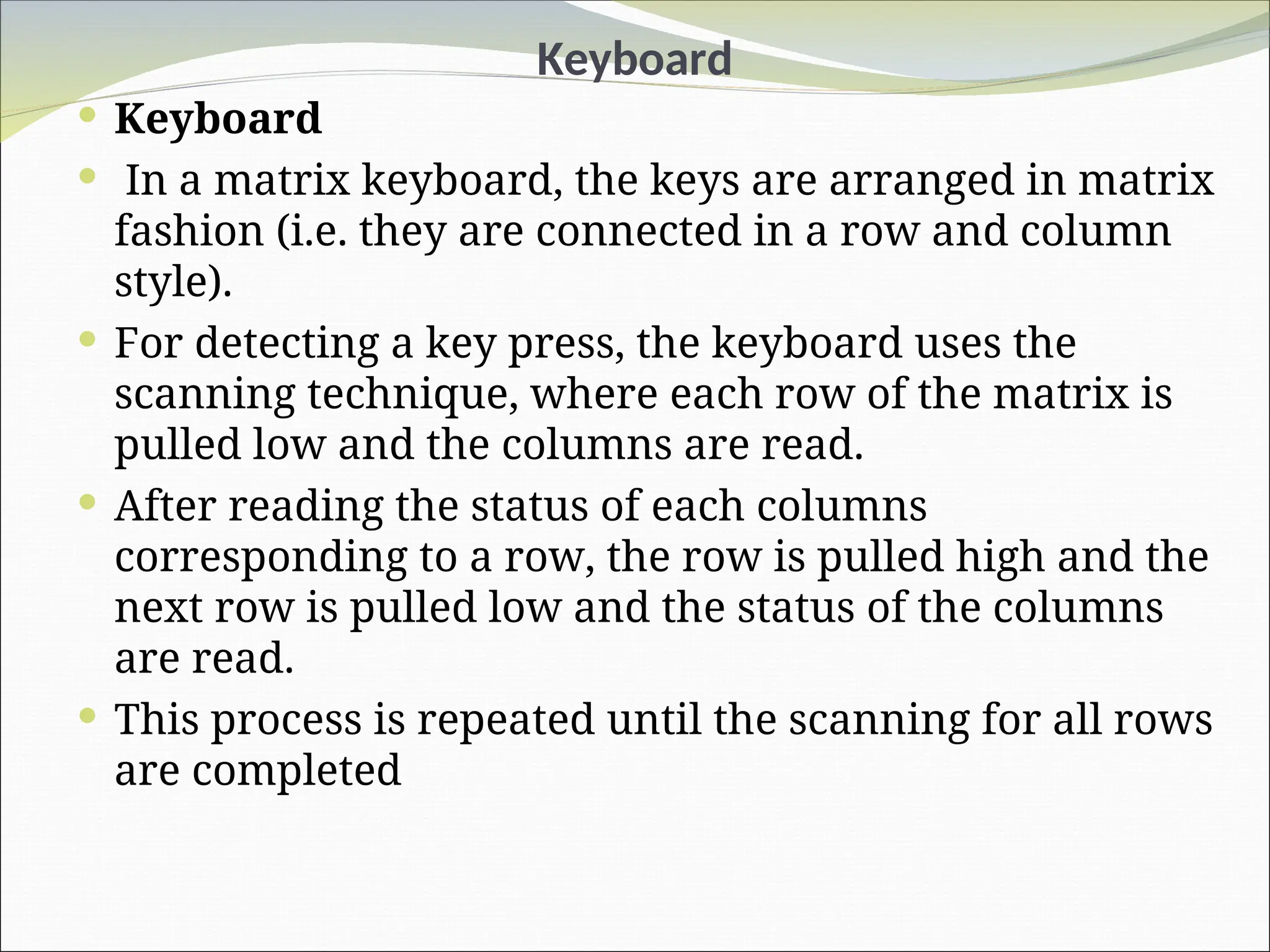
Keyboard
Ina matrix keyboard, the keys are arranged in matrix
fashion (i.e. they are connected in a row and column
style).
For detecting a key press, the keyboard uses the
scanning technique, where each row of the matrix is
pulled low and the columns are read.
After reading the status of each columns
corresponding to a row, the row is pulled high and the
next row is pulled low and the status of the columns
are read.
This process is repeated until the scanning for all rows
are completed
116.
Communication Interface
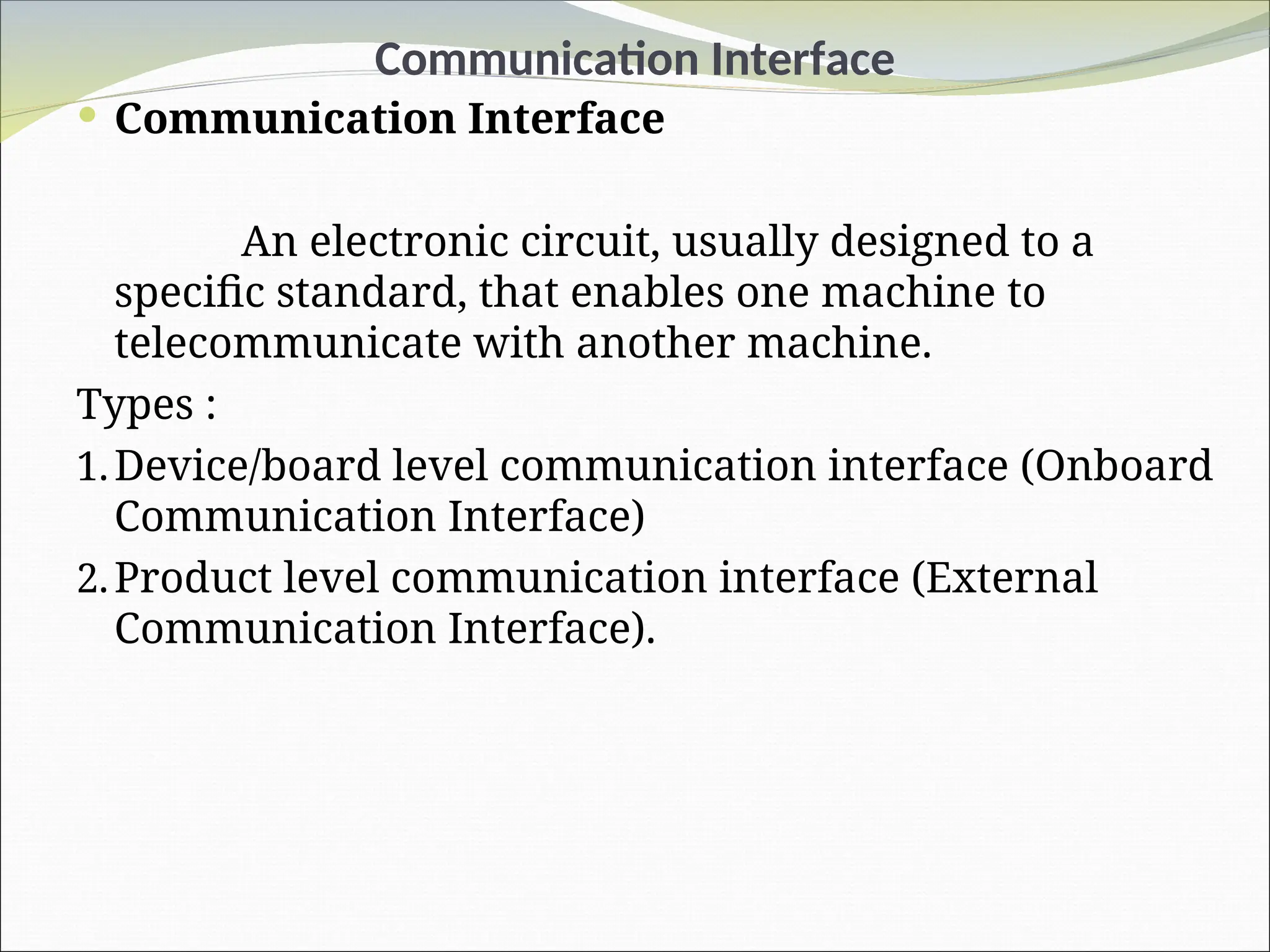
CommunicationInterface
An electronic circuit, usually designed to a
specific standard, that enables one machine to
telecommunicate with another machine.
Types :
1.Device/board level communication interface (Onboard
Communication Interface)
2.Product level communication interface (External
Communication Interface).
117.
Communication Interface
1. Device/boardlevel communication interface
(Onboard Communication Interface)
The communication channel which interconnects
the various components within an embedded
product is referred as device/board level
2.Product level communication interface (External
Communication Interface).
It is responsible for data transfer between the
embedded system and other devices or modules
118.
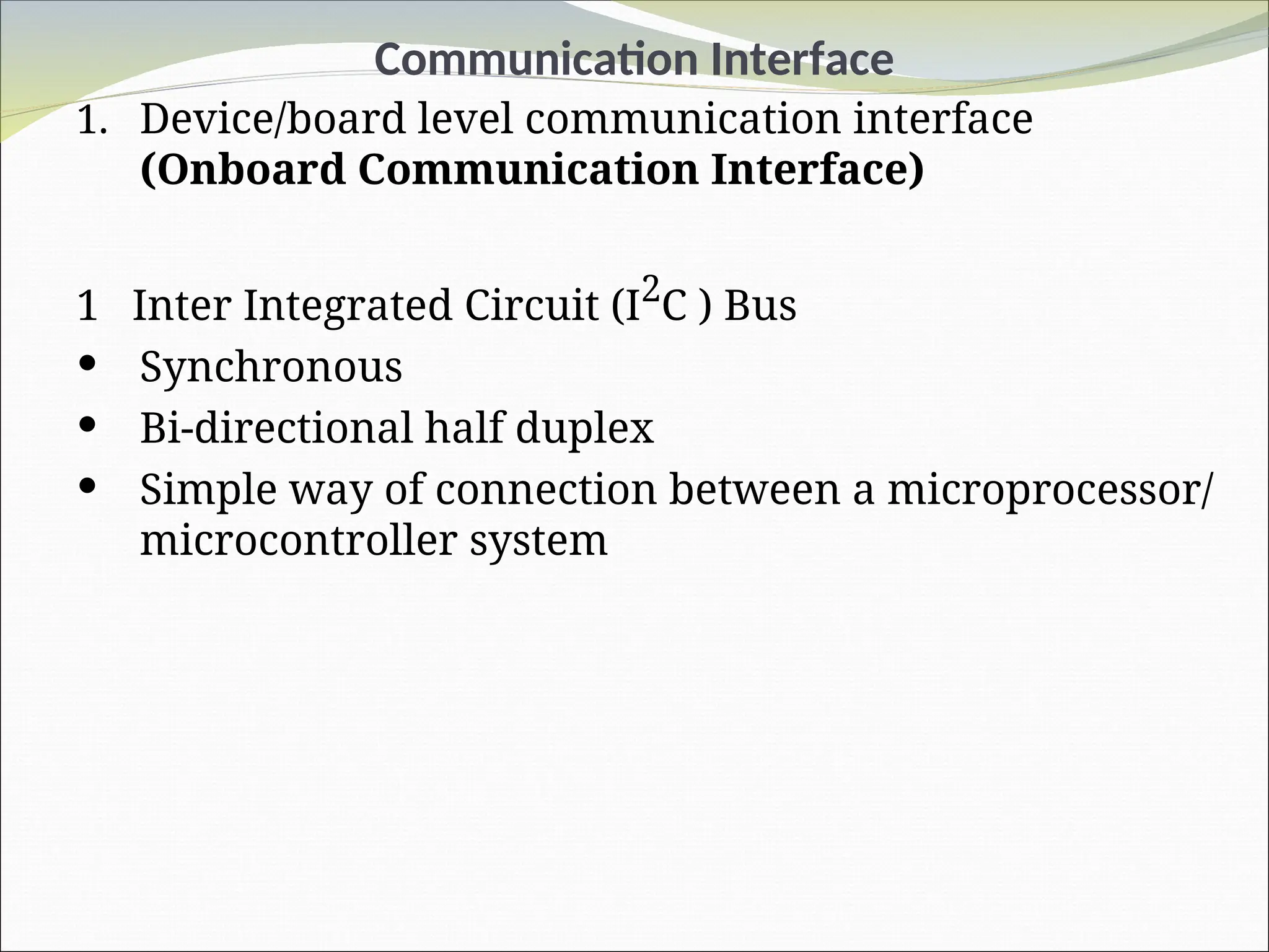
Communication Interface
1. Device/boardlevel communication interface
(Onboard Communication Interface)
1 Inter Integrated Circuit (I2
C ) Bus
Synchronous
Bi-directional half duplex
Simple way of connection between a microprocessor/
microcontroller system
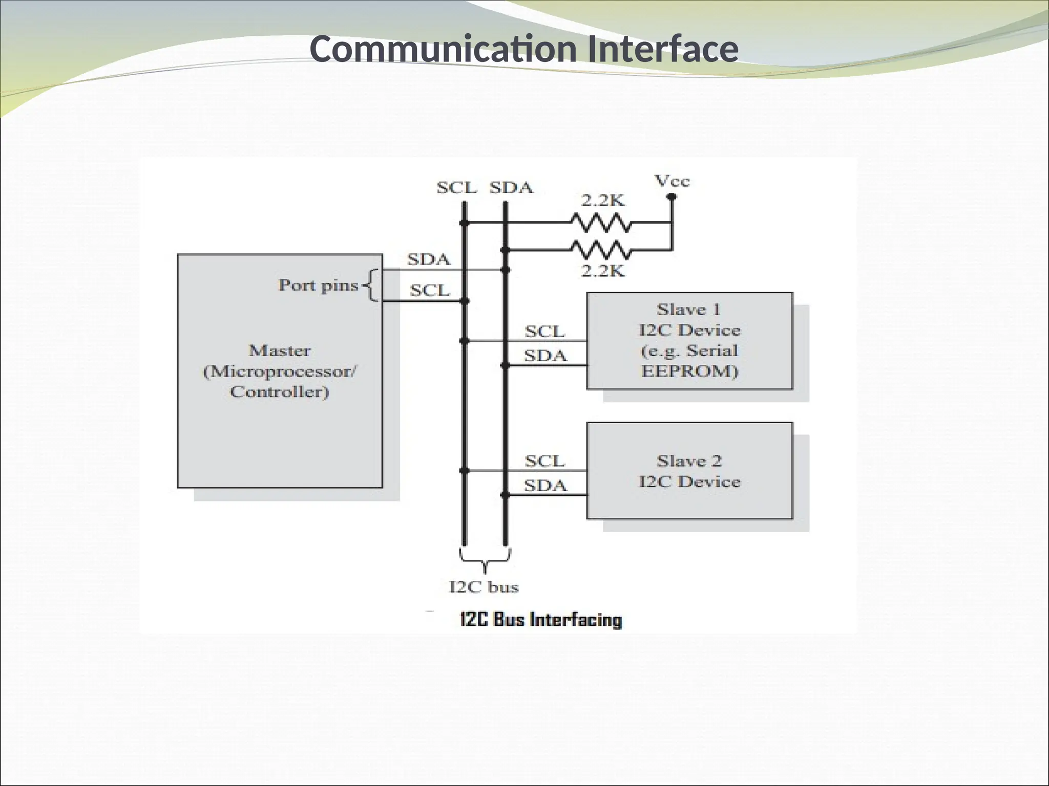
Communication Interface
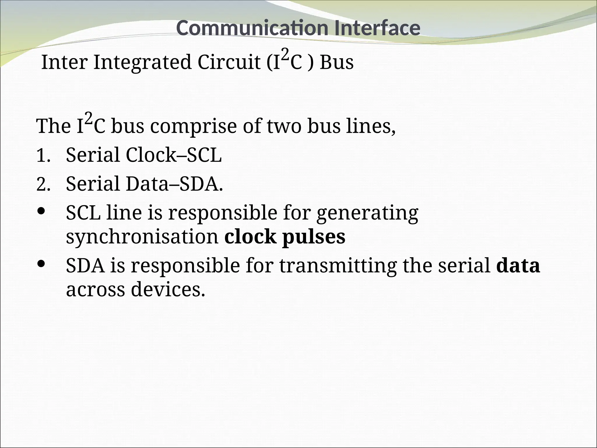
Inter IntegratedCircuit (I2
C ) Bus
The I2
C bus comprise of two bus lines,
1. Serial Clock–SCL
2. Serial Data–SDA.
SCL line is responsible for generating
synchronisation clock pulses
SDA is responsible for transmitting the serial data
across devices.
121.
Communication Interface
Inter IntegratedCircuit (I2
C ) Bus
I2
C bus is a shared bus system to which many
number of I2
C devices can be connected.
Devices connected to the I2C bus can act as either
‘Master’ device or ‘Slave’ device.
The ‘Master’ device is responsible for controlling the
communication by initiating/terminating data
transfer, sending data and generating necessary
synchronisation clock pulses.
‘Slave’ devices wait for the commands from the
master and respond upon receiving the commands
122.
Communication Interface
Inter IntegratedCircuit (I2
C ) Bus
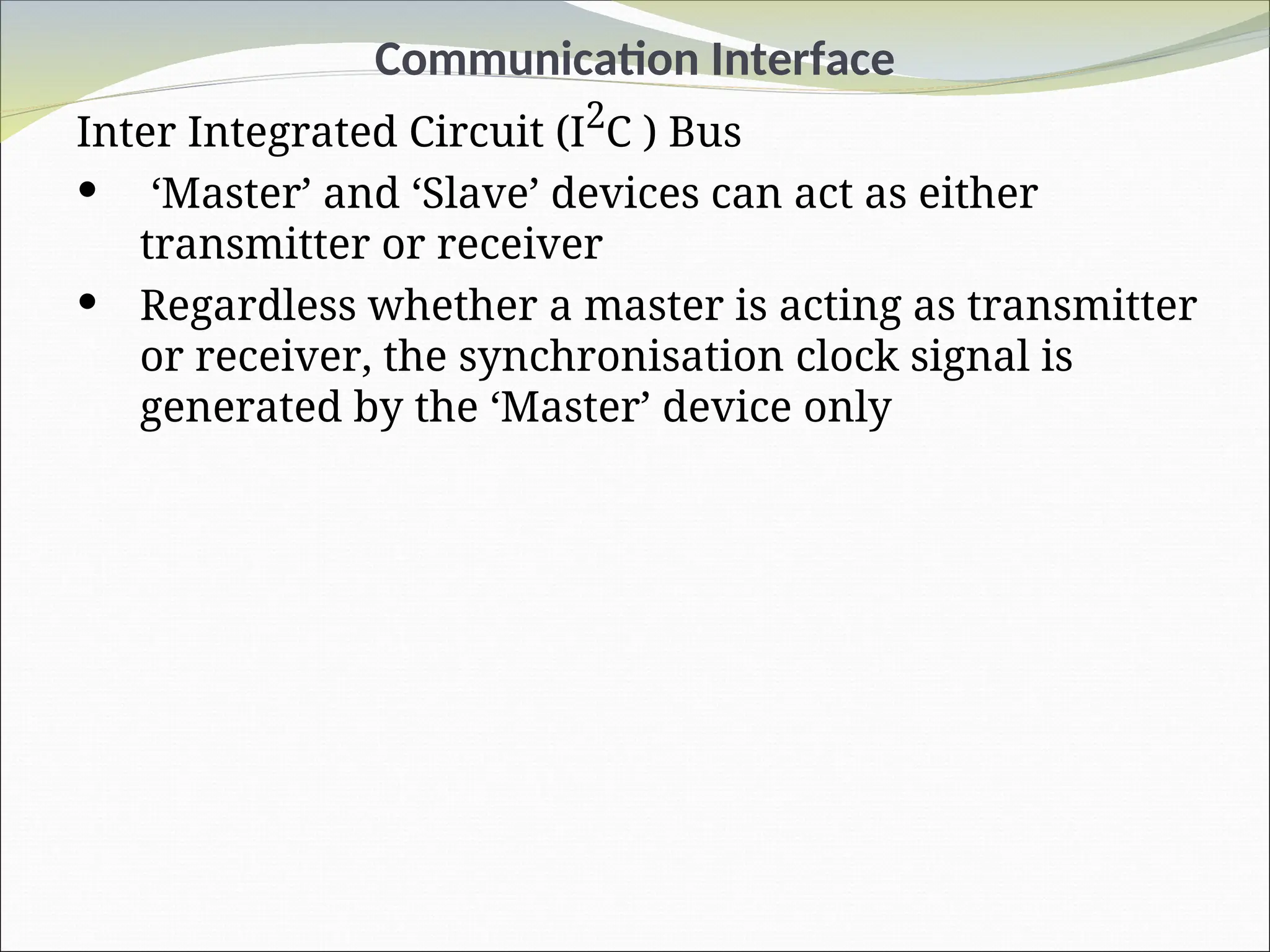
‘Master’ and ‘Slave’ devices can act as either
transmitter or receiver
Regardless whether a master is acting as transmitter
or receiver, the synchronisation clock signal is
generated by the ‘Master’ device only
123.
Communication Interface
Inter IntegratedCircuit (I2
C ) Bus
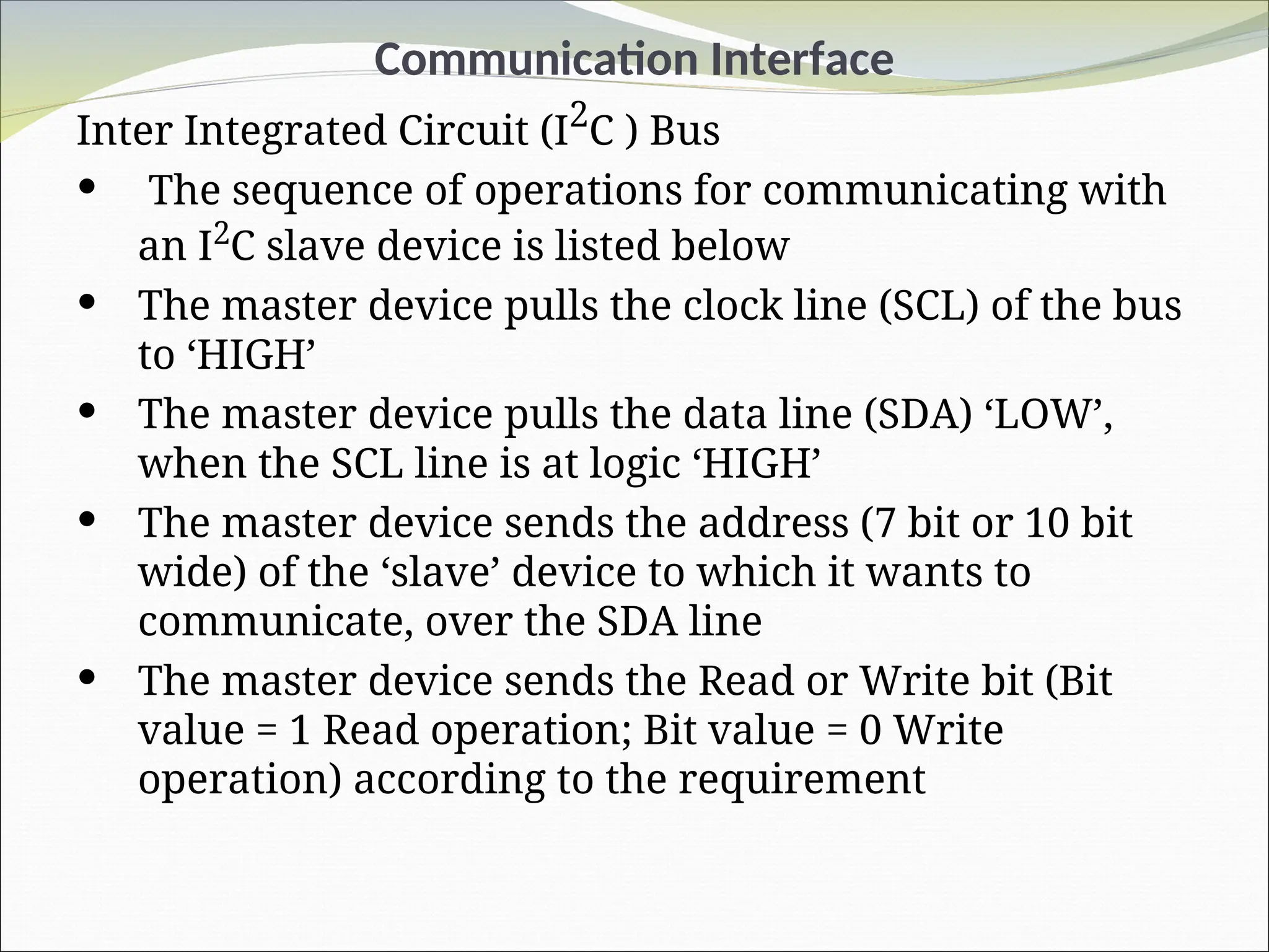
The sequence of operations for communicating with
an I2
C slave device is listed below
The master device pulls the clock line (SCL) of the bus
to ‘HIGH’
The master device pulls the data line (SDA) ‘LOW’,
when the SCL line is at logic ‘HIGH’
The master device sends the address (7 bit or 10 bit
wide) of the ‘slave’ device to which it wants to
communicate, over the SDA line
The master device sends the Read or Write bit (Bit
value = 1 Read operation; Bit value = 0 Write
operation) according to the requirement
124.
Communication Interface
Inter IntegratedCircuit (I2
C ) Bus
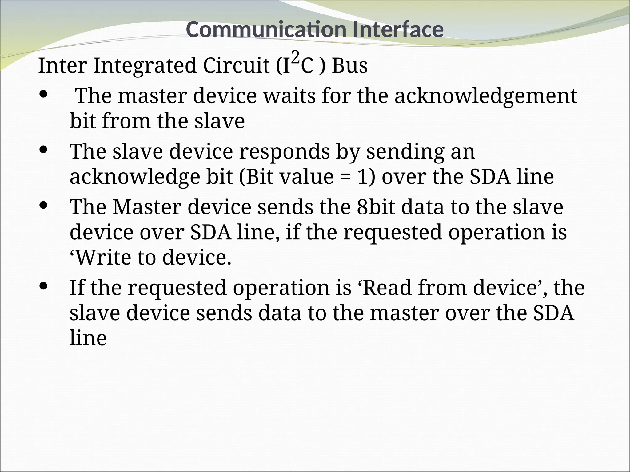
The master device waits for the acknowledgement
bit from the slave
The slave device responds by sending an
acknowledge bit (Bit value = 1) over the SDA line
The Master device sends the 8bit data to the slave
device over SDA line, if the requested operation is
‘Write to device.
If the requested operation is ‘Read from device’, the
slave device sends data to the master over the SDA
line
125.
Communication Interface
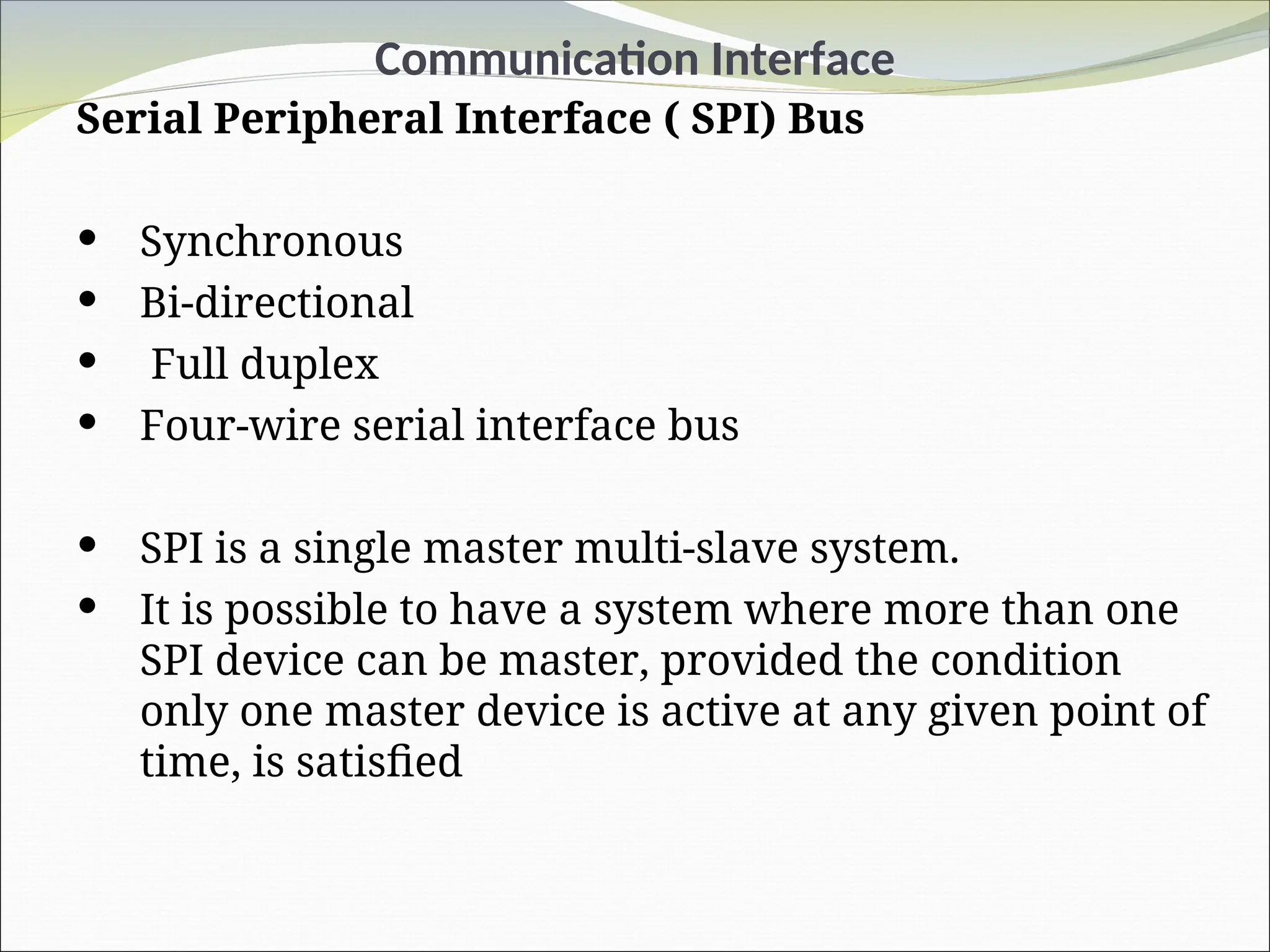
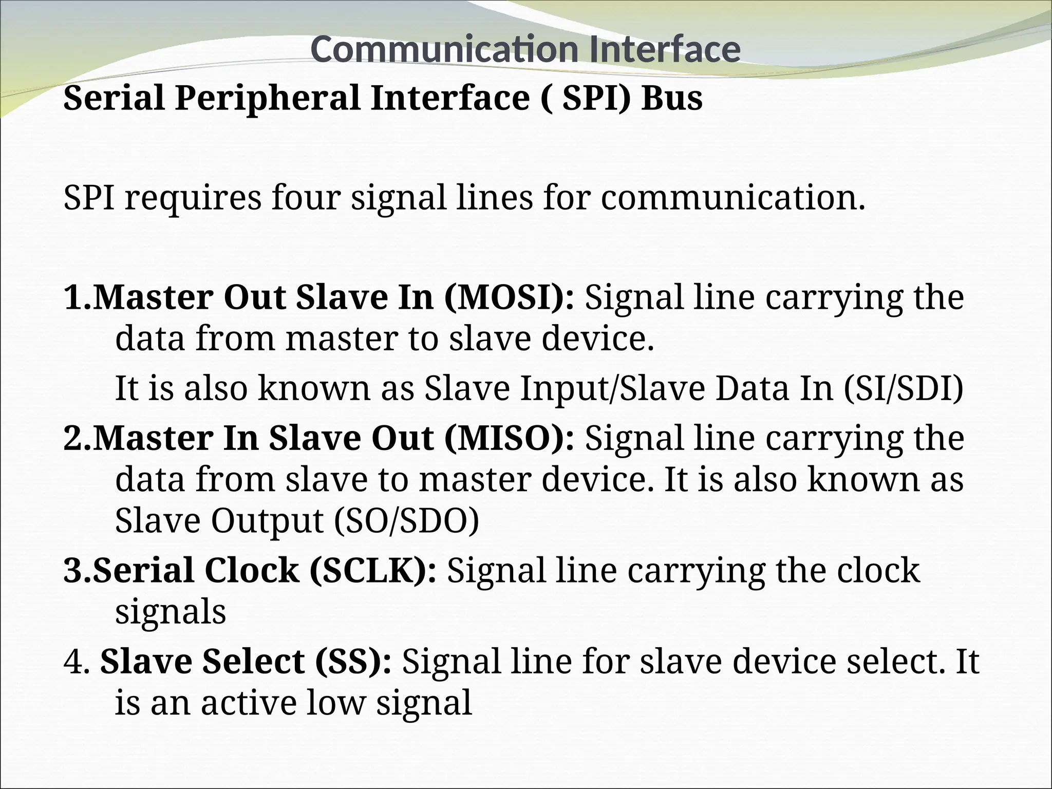
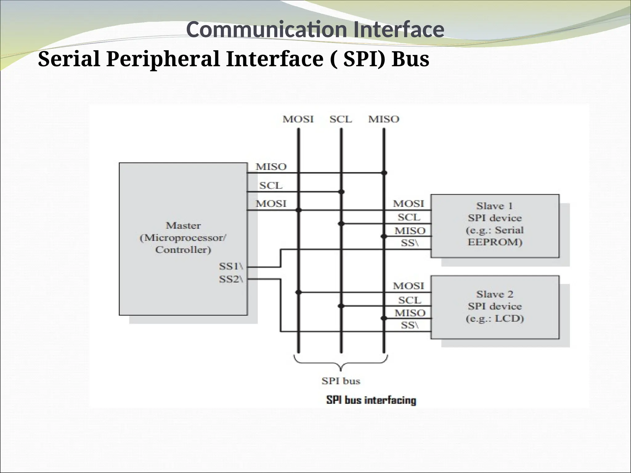
Serial PeripheralInterface ( SPI) Bus
Synchronous
Bi-directional
Full duplex
Four-wire serial interface bus
SPI is a single master multi-slave system.
It is possible to have a system where more than one
SPI device can be master, provided the condition
only one master device is active at any given point of
time, is satisfied
126.
Communication Interface
Serial PeripheralInterface ( SPI) Bus
SPI requires four signal lines for communication.
1.Master Out Slave In (MOSI): Signal line carrying the
data from master to slave device.
It is also known as Slave Input/Slave Data In (SI/SDI)
2.Master In Slave Out (MISO): Signal line carrying the
data from slave to master device. It is also known as
Slave Output (SO/SDO)
3.Serial Clock (SCLK): Signal line carrying the clock
signals
4. Slave Select (SS): Signal line for slave device select. It
is an active low signal
Communication Interface
Serial PeripheralInterface ( SPI) Bus
The master device is responsible for generating the
clock signal.
It selects the required slave device by making the
corresponding slave device’s slave select signal ‘LOW’
SPI works on the principle of ‘Shift Register
During transmission from the master to slave, the
data in the master’s shift register is shifted out to the
MOSI pin and it enters the shift register of the slave
device through the MOSI pin of the slave device.
At the same time the shifted out data bit from the
slave device’s shift register enters the shift register of
the master device through MISO pin
129.
Communication Interface
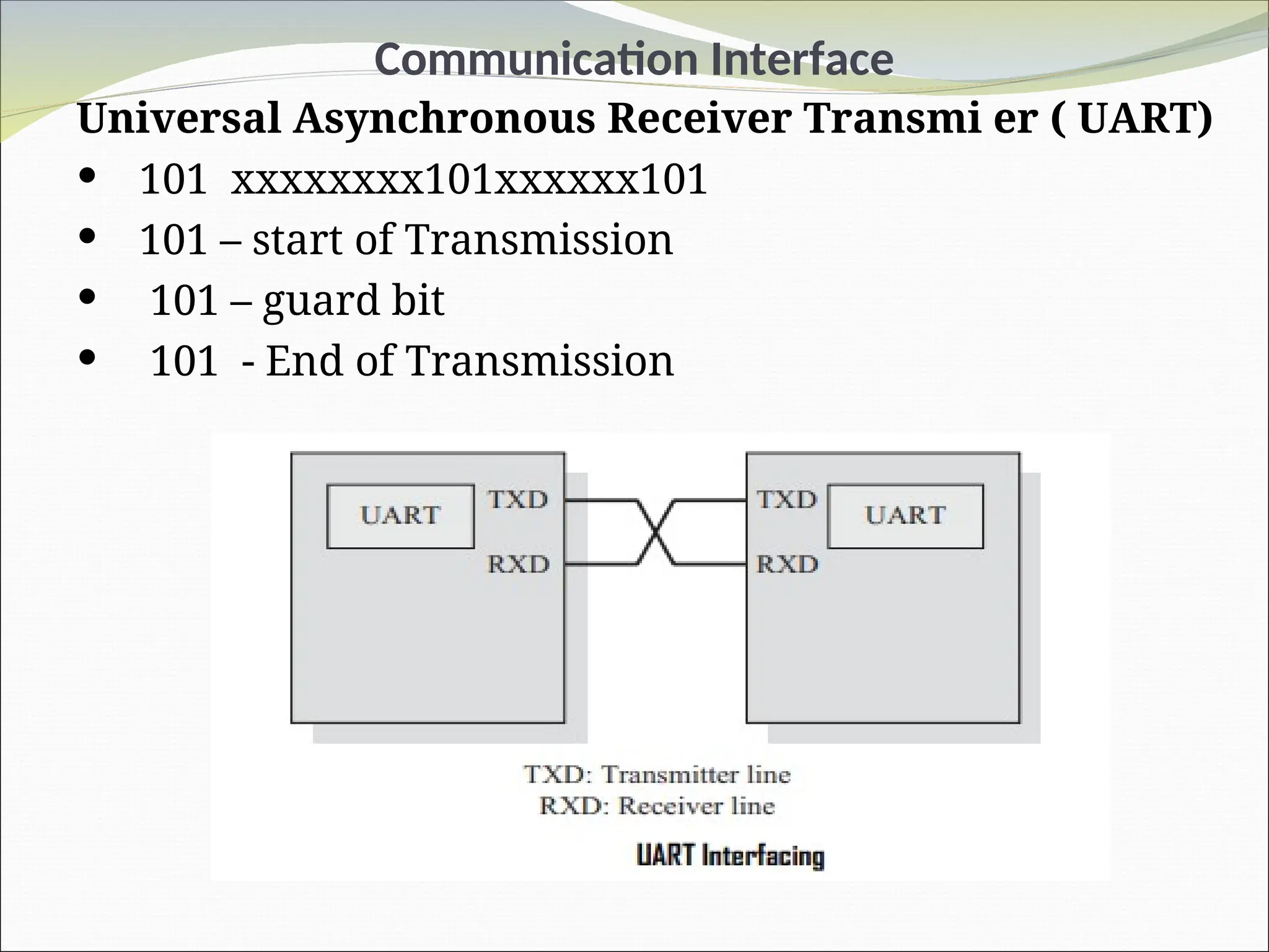
Universal AsynchronousReceiver Transmi er ( UART)
It is an asynchronous form of serial data transmission.
UART based serial data transmission doesn’t require a
clock signal to synchronise the transmitting end and
receiving end for transmission.
Instead it relies upon the pre-defined agreement
between the transmitting device and receiving device.
The start and stop of communication is indicated
through inserting special bits in the data stream.
While sending a byte of data, a start bit is added first
and a stop bit is added at the end of the bit stream.
The least signifi cant bit of the data byte follows the
‘start’ bit.
Communication Interface
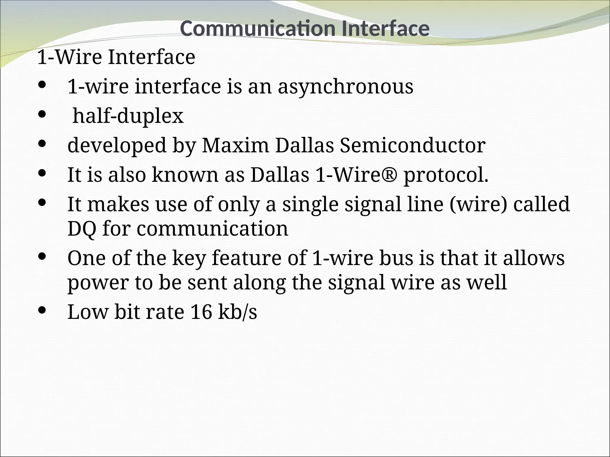
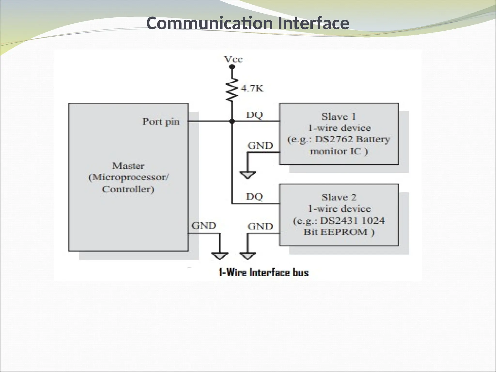
1-Wire Interface
1-wire interface is an asynchronous
half-duplex
developed by Maxim Dallas Semiconductor
It is also known as Dallas 1-Wire® protocol.
It makes use of only a single signal line (wire) called
DQ for communication
One of the key feature of 1-wire bus is that it allows
power to be sent along the signal wire as well
Low bit rate 16 kb/s
Communication Interface
1-Wire Interface
The 1-Wire slave devices incorporate internal
capacitor (typically of the order of 800 pF) to power
the device from the signal line.
The 1-wire interface supports a single master and
one or more slave devices on the bus
134.
Communication Interface
1-Wire Interface
The sequence of operation :
1. The master device sends a ‘Reset’ pulse on the 1-
wire bus. 2. The slave device(s) present on the bus
respond with a
‘Presence’ pulse.
3. The master device sends a ROM command.
This addresses the slave device(s) to which it wants
to
initiate a communication.
4. The master device sends a read/write function
command to read/write the internal memory or
register of the slave device.
135.
Communication Interface
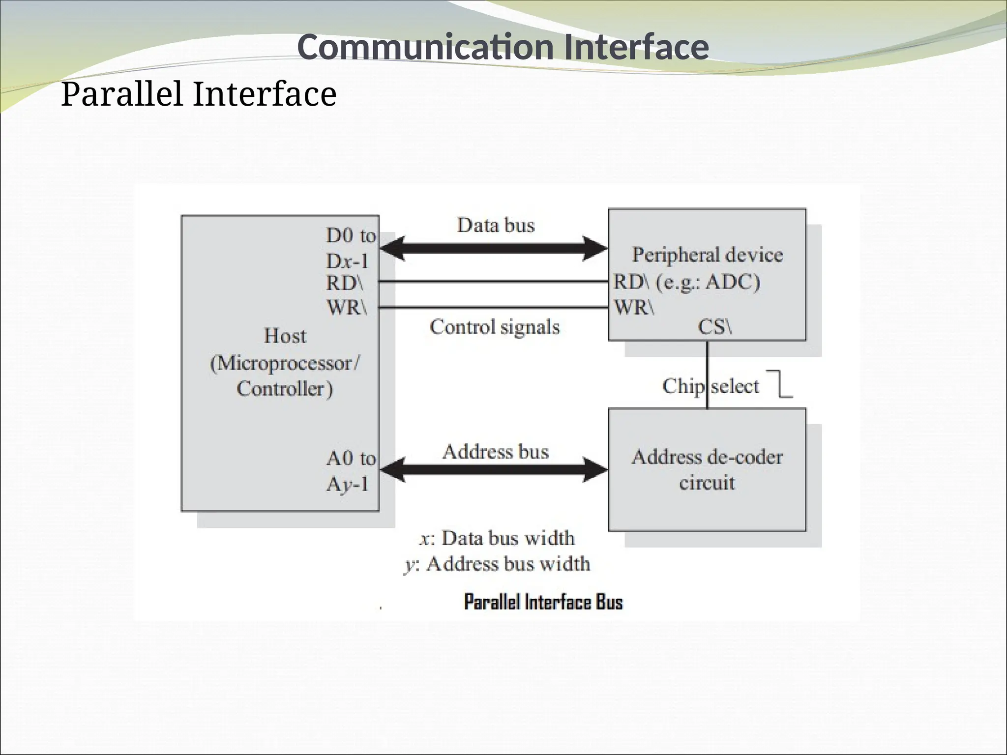
Parallel Interface
Used for communicating with peripheral devices which
are memory mapped (primary memory)to the host of
the system - Mouse,Key Board,projector,USB,HDD,Flash
Memory , Printer, Monitor,Speakers
The device which supports parallel bus can directly
connect to this bus system – hub processor/ controller
The communication through the parallel bus is
controlled by the control signal interface between the
device and the host.
The ‘Control Signals’ for communication includes
‘Read/Write’ signal and device select signal.
The device normally contains a device select line and
the device becomes active only when this line is
asserted by the host processor.
Communication Interface
Parallel Interface
The direction of data transfer (Host to Device or
Device to Host) can be controlled through the control
signal lines for ‘Read’ and ‘Write’
An address decoder circuit is used for generating the
chip select signal for the device
When the address selected by the processor is within
the range assigned for the device, the decoder circuit
activates the chip select line and thereby the device
becomes active.
The processor then can read or write from or to the
device
corresponding control line (RD and WR
respectively)
138.
Communication Interface
RS-232 C& RS-485
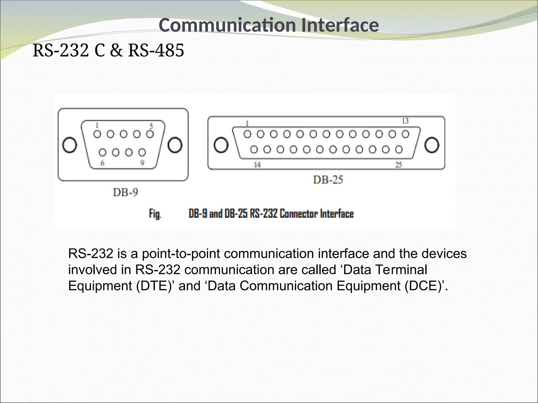
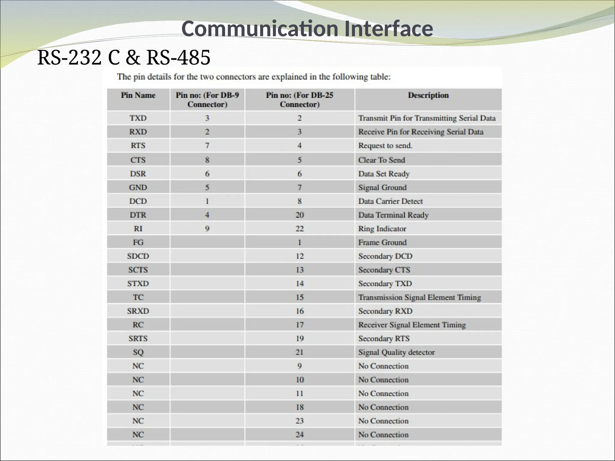
RS-232 C (Recommended Standard number 232
revision C from the Electronic Industry Association) is a
legacy, full duplex, wired, asynchronous serial
communication interface.
The RS-232 interface is developed by the Electronics
Industries Association (EIA) during the early 1960s
UART uses the standard TTL/CMOS logic (Logic ‘High’
corresponds to bit value 1 and Logic ‘Low’ corresponds
to bit value 0) for bit transmission whereas RS-232
follows the EIA standard for bit transmission.
TTL - Transistor – Transistor Logic
DTL – Diode Transistor Logic
RTL Resistor – Transistor Logic
CMOS – Complementary Metal Oxide Semi Conductor
139.
Communication Interface
RS-232 C& RS-485
As per the EIA standard, a logic ‘0’ is represented
with voltage between +3 and +25V and a logic ‘1’ is
represented with voltage between –3 and –25V.
In EIA standard, logic ‘0’ is known as ‘Space’ and
logic ‘1’ as ‘Mark’.
The RS-232 interface defi nes various handshaking
and control signals for communication apart from
the ‘Transmit’ and ‘Receive’ signal lines for data
communication
140.
Communication Interface
RS-232 C& RS-485
RS-232 is a point-to-point communication interface and the devices
involved in RS-232 communication are called ‘Data Terminal
Equipment (DTE)’ and ‘Data Communication Equipment (DCE)’.
Communication Interface
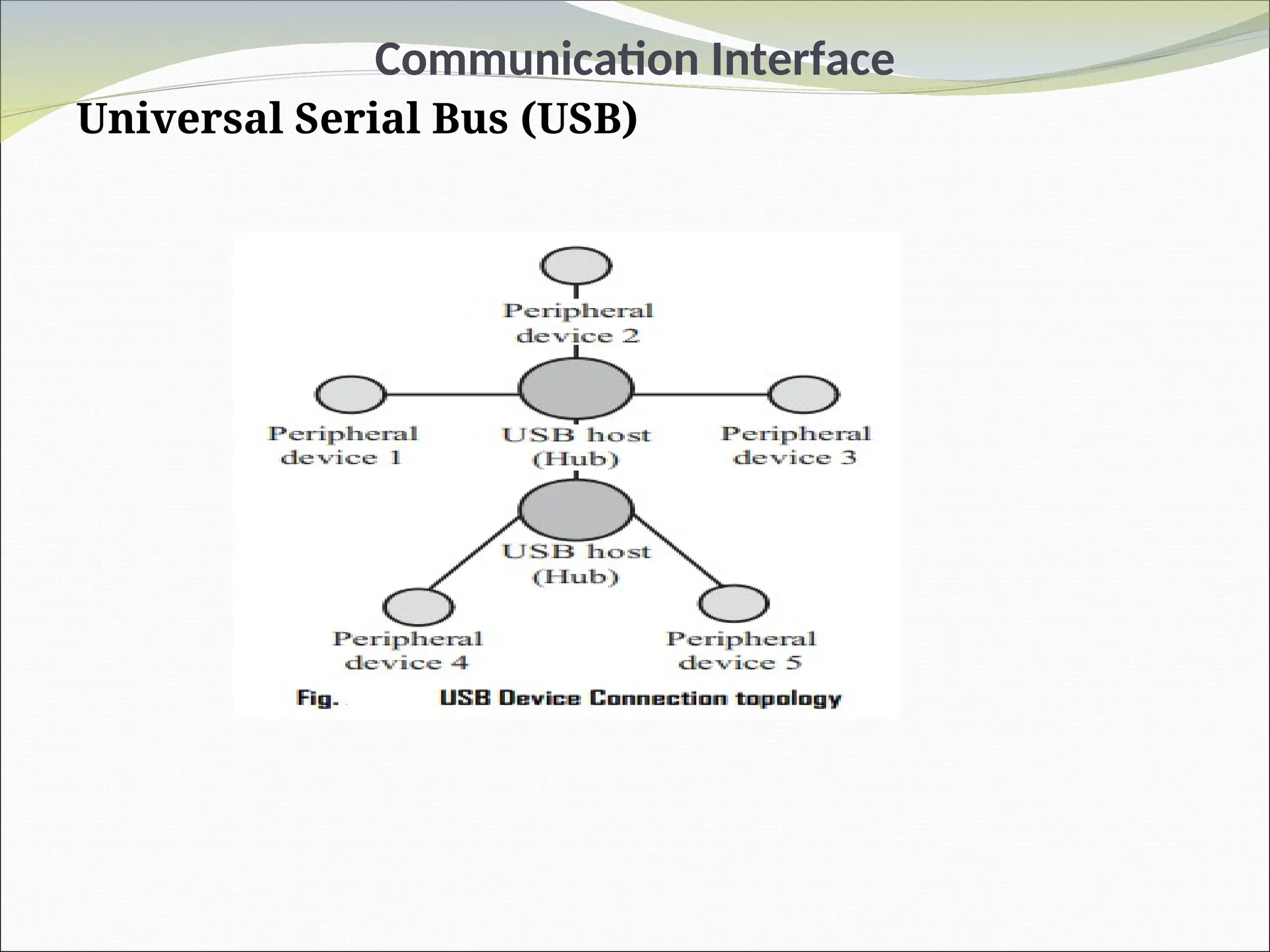
Universal SerialBus (USB)
Universal Serial Bus ( USB) is a wired high speed serial
bus for data communication.
The first version of USB (USB1.0) was released in 1995.
created by the USB core group members consisting of
Intel, Microsoft, IBM.
The USB communication system follows a star
topology with a USB host at the centre and one or
more USB peripheral devices/USB hosts connected to
it.
A USB 2.0 host can support connections up to 127,
including slave peripheral devices and other USB
hosts
Communication Interface
Universal SerialBus (USB)
The USB host contains a host controller which is
responsible for controlling the data communication,
Also establishing connectivity with USB slave devices,
packetizing.
The USB cable in USB 2.0 specifi cation supports
communication distance of up to 5 meters.
The USB 2.0 standard uses two different types of
connector at the ends of the USB cable for connecting
the USBperipheral device and host device.
‘Type A’ connector is used for upstream connection
(connection with host) and Type B or Mini/Micro USB
connector is used for downstream connection
(connection with slave device)
145.
Communication Interface
Universal SerialBus (USB)
The USB host contains a host controller which is
responsible for controlling the data communication,
Also establishing connectivity with USB slave
devices, packetizing.
The USB cable in USB 2.0 specifi cation supports
communication distance of up to 5 meters.
The USB 2.0 standard uses two different types of
connector at the ends of the USB cable for connecting
the USB
146.
Communication Interface
Universal SerialBus (USB)
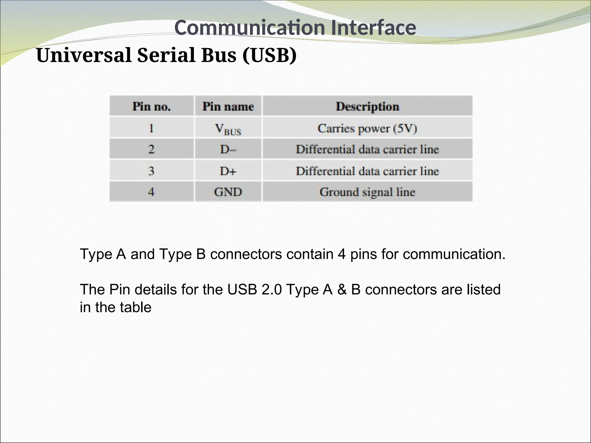
Type A and Type B connectors contain 4 pins for communication.
The Pin details for the USB 2.0 Type A & B connectors are listed
in the table
147.
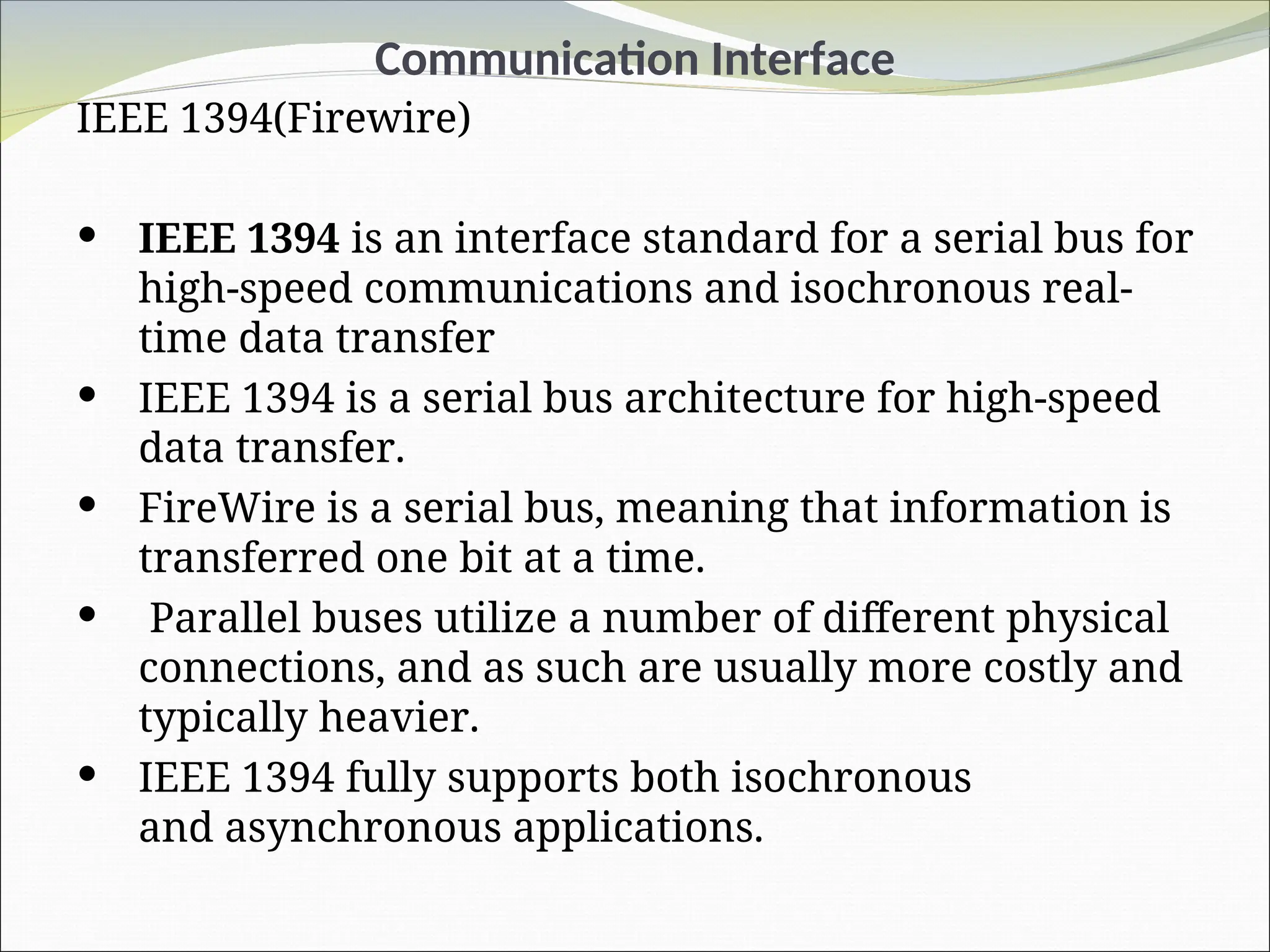
Communication Interface
IEEE 1394(Firewire)
IEEE 1394 is an interface standard for a serial bus for
high-speed communications and isochronous real-
time data transfer
IEEE 1394 is a serial bus architecture for high-speed
data transfer.
FireWire is a serial bus, meaning that information is
transferred one bit at a time.
Parallel buses utilize a number of different physical
connections, and as such are usually more costly and
typically heavier.
IEEE 1394 fully supports both isochronous
and asynchronous applications.
148.
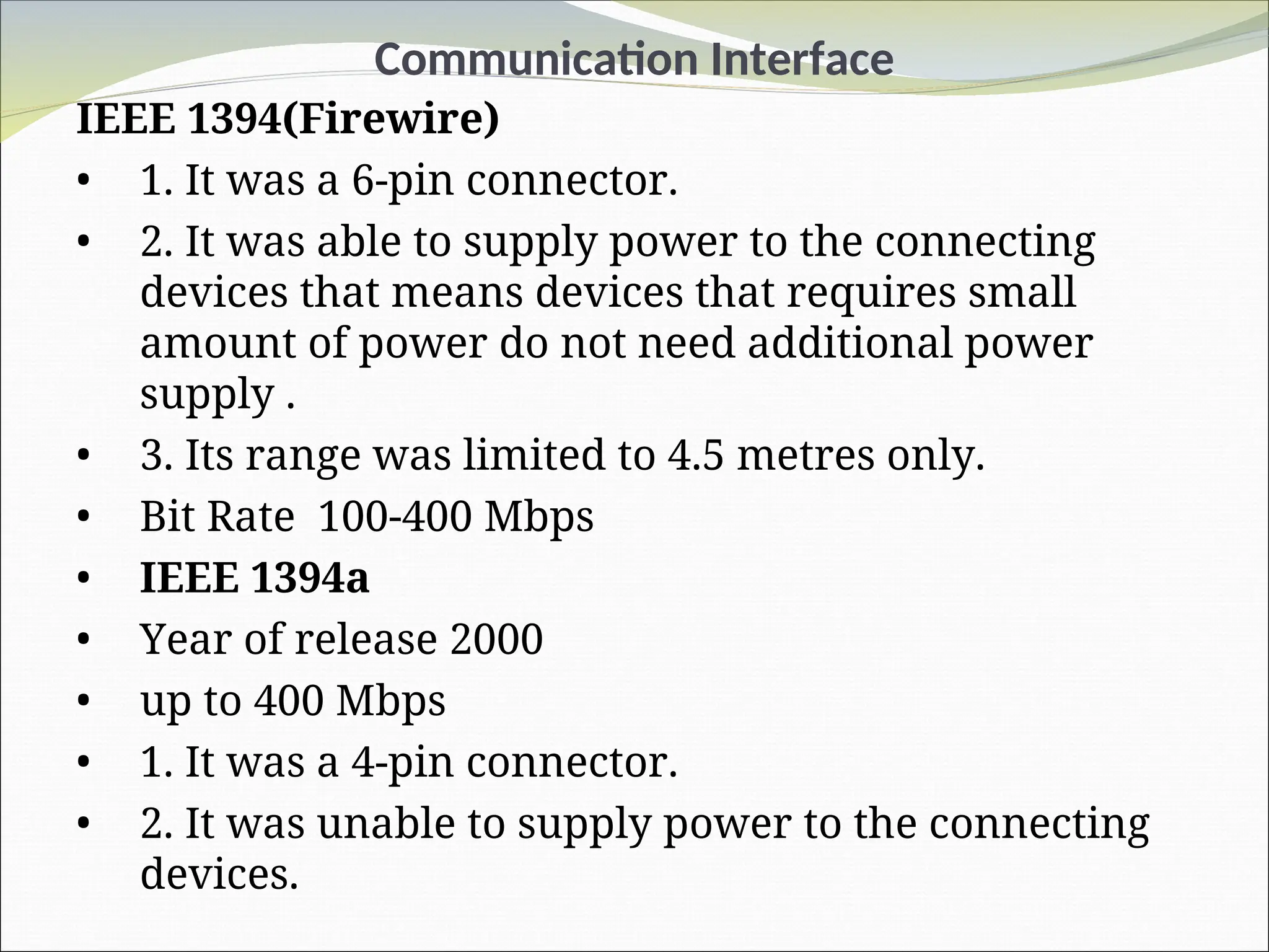
Communication Interface
IEEE 1394(Firewire)
•1. It was a 6-pin connector.
• 2. It was able to supply power to the connecting
devices that means devices that requires small
amount of power do not need additional power
supply .
• 3. Its range was limited to 4.5 metres only.
• Bit Rate 100-400 Mbps
• IEEE 1394a
• Year of release 2000
• up to 400 Mbps
• 1. It was a 4-pin connector.
• 2. It was unable to supply power to the connecting
devices.
149.
Communication Interface
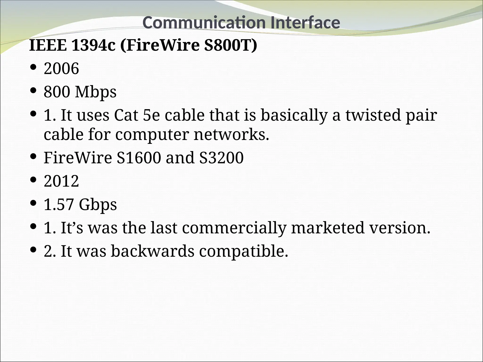
IEEE 1394c(FireWire S800T)
2006
800 Mbps
1. It uses Cat 5e cable that is basically a twisted pair
cable for computer networks.
FireWire S1600 and S3200
2012
1.57 Gbps
1. It’s was the last commercially marketed version.
2. It was backwards compatible.
150.
Communication Interface
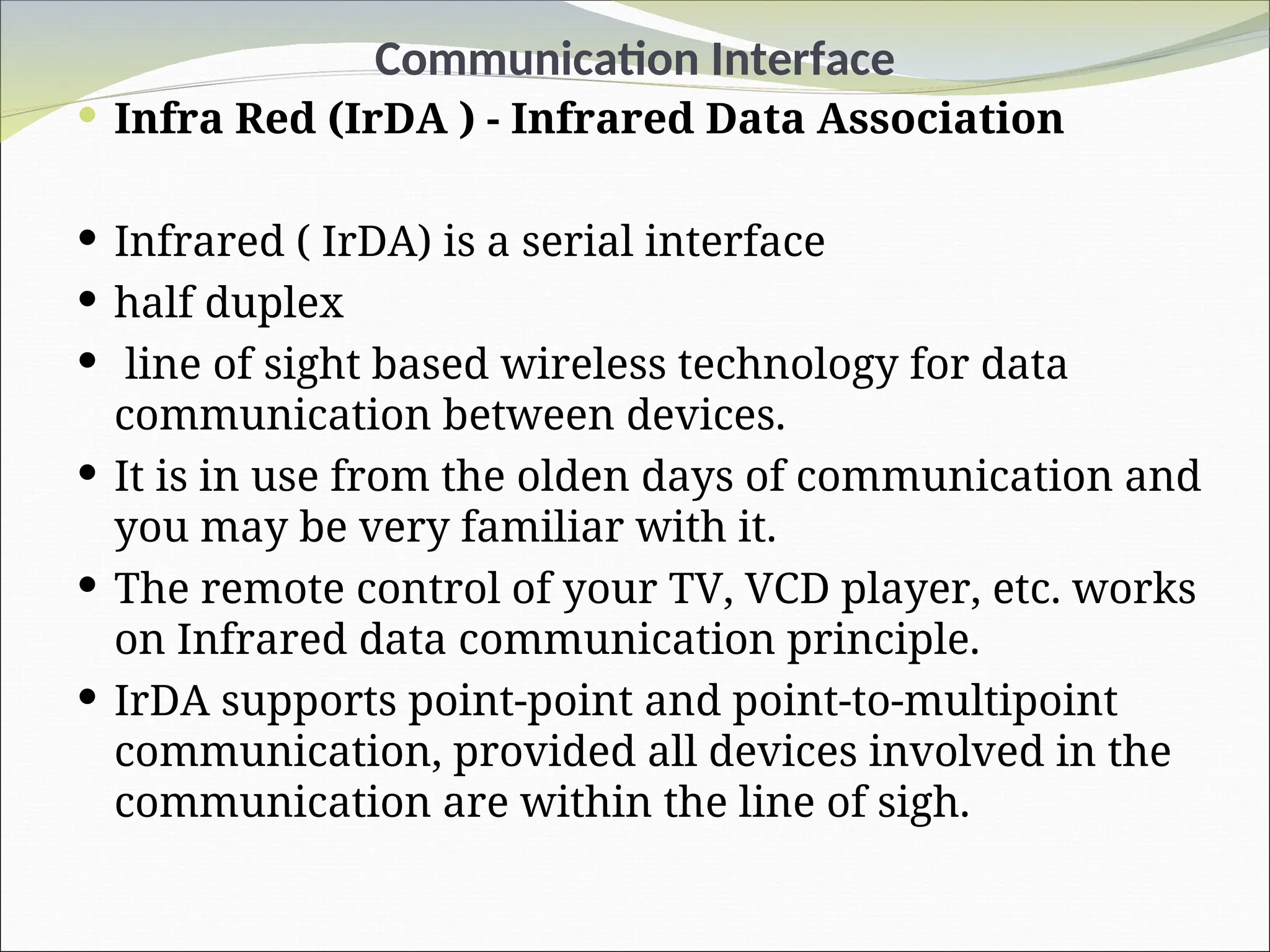
InfraRed (IrDA ) - Infrared Data Association
Infrared ( IrDA) is a serial interface
half duplex
line of sight based wireless technology for data
communication between devices.
It is in use from the olden days of communication and
you may be very familiar with it.
The remote control of your TV, VCD player, etc. works
on Infrared data communication principle.
IrDA supports point-point and point-to-multipoint
communication, provided all devices involved in the
communication are within the line of sigh.
151.
Communication Interface
Infrared(IrDA)
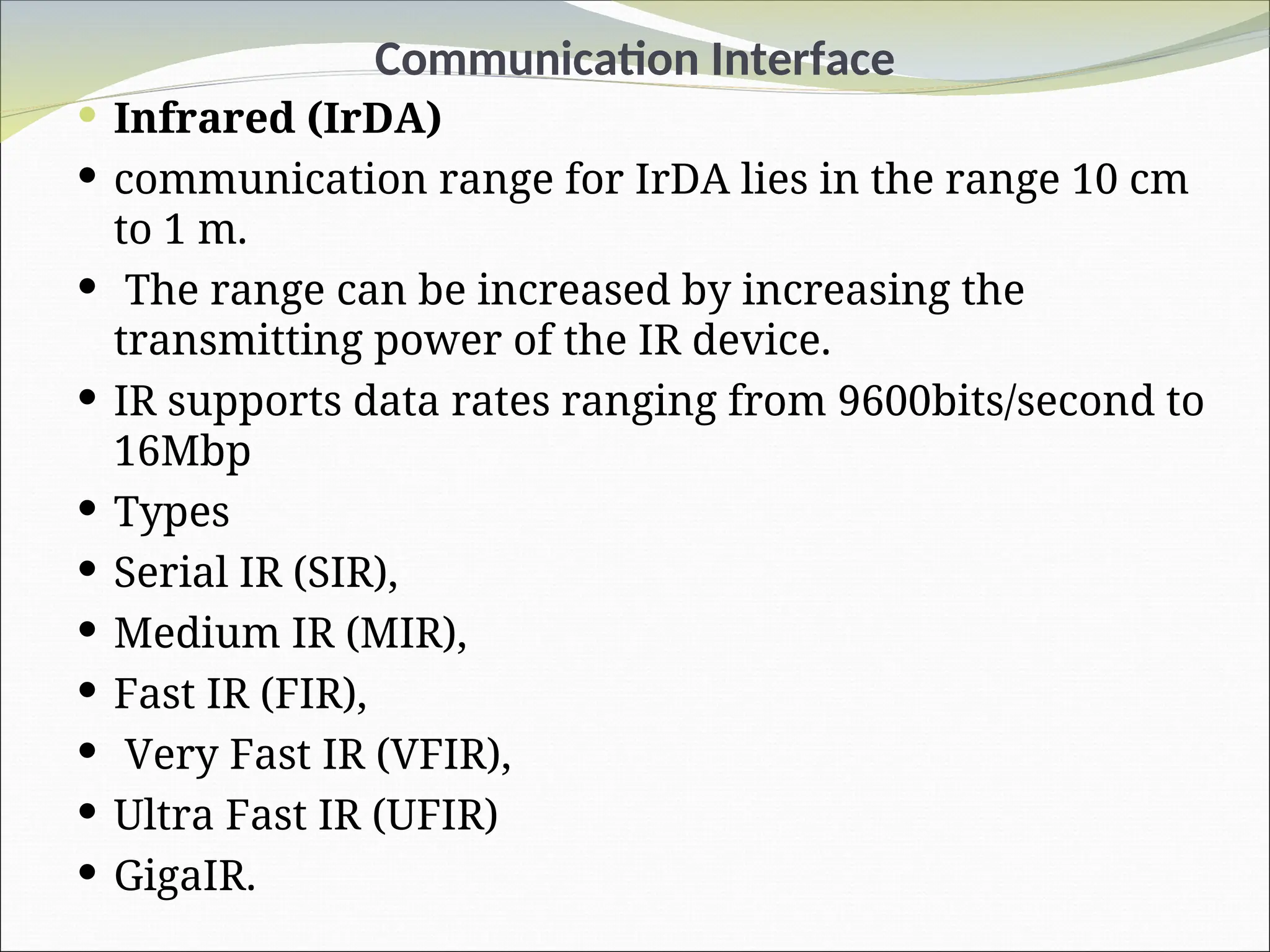
communication range for IrDA lies in the range 10 cm
to 1 m.
The range can be increased by increasing the
transmitting power of the IR device.
IR supports data rates ranging from 9600bits/second to
16Mbp
Types
Serial IR (SIR),
Medium IR (MIR),
Fast IR (FIR),
Very Fast IR (VFIR),
Ultra Fast IR (UFIR)
GigaIR.
152.
Communication Interface
Infrared(IrDA)
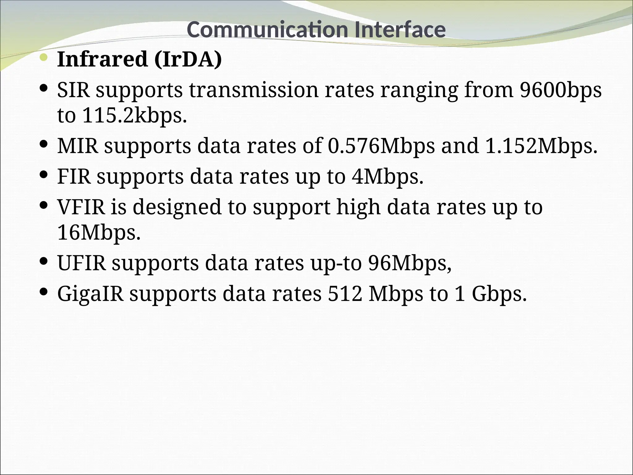
SIR supports transmission rates ranging from 9600bps
to 115.2kbps.
MIR supports data rates of 0.576Mbps and 1.152Mbps.
FIR supports data rates up to 4Mbps.
VFIR is designed to support high data rates up to
16Mbps.
UFIR supports data rates up-to 96Mbps,
GigaIR supports data rates 512 Mbps to 1 Gbps.
153.
Communication Interface
Infrared(IrDA)
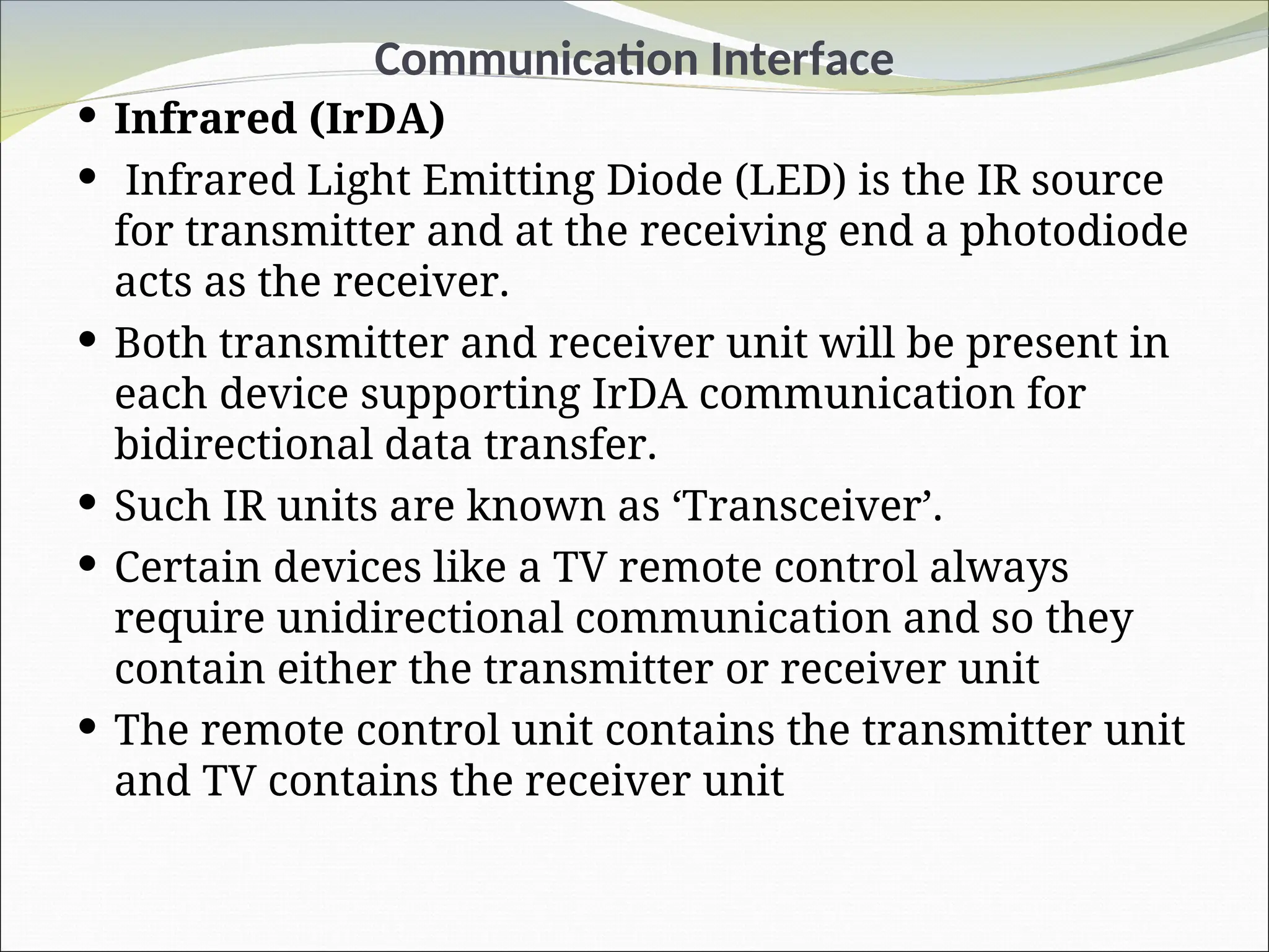
Infrared Light Emitting Diode (LED) is the IR source
for transmitter and at the receiving end a photodiode
acts as the receiver.
Both transmitter and receiver unit will be present in
each device supporting IrDA communication for
bidirectional data transfer.
Such IR units are known as ‘Transceiver’.
Certain devices like a TV remote control always
require unidirectional communication and so they
contain either the transmitter or receiver unit
The remote control unit contains the transmitter unit
and TV contains the receiver unit
154.
Communication Interface
Bluetooth(BT)
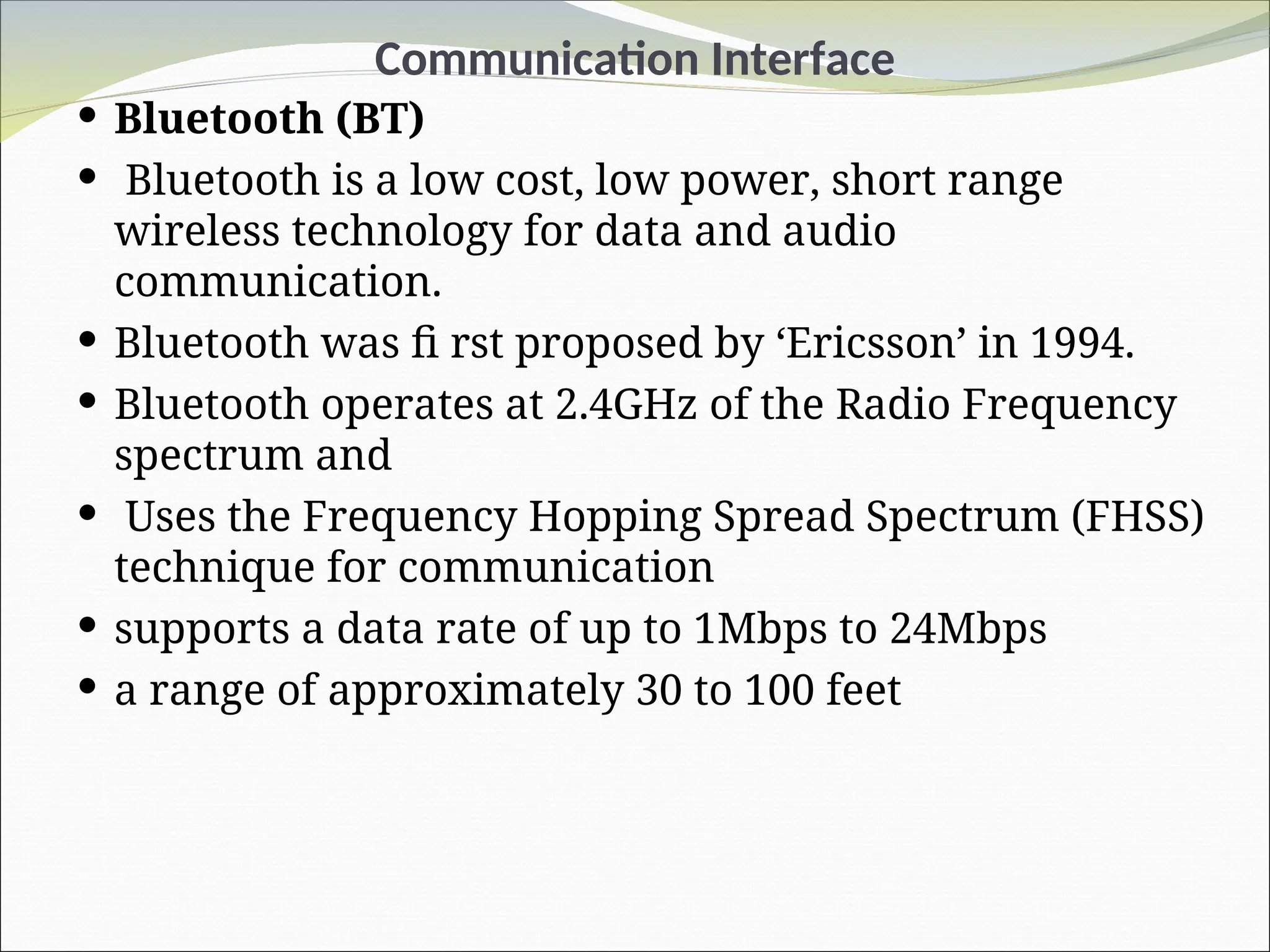
Bluetooth is a low cost, low power, short range
wireless technology for data and audio
communication.
Bluetooth was fi rst proposed by ‘Ericsson’ in 1994.
Bluetooth operates at 2.4GHz of the Radio Frequency
spectrum and
Uses the Frequency Hopping Spread Spectrum (FHSS)
technique for communication
supports a data rate of up to 1Mbps to 24Mbps
a range of approximately 30 to 100 feet
155.
Communication Interface
Bluetooth(BT)
Bluetooth Architecture:
The architecture of Bluetooth defines two types of
networks:
1. Piconet
2. Scatternet
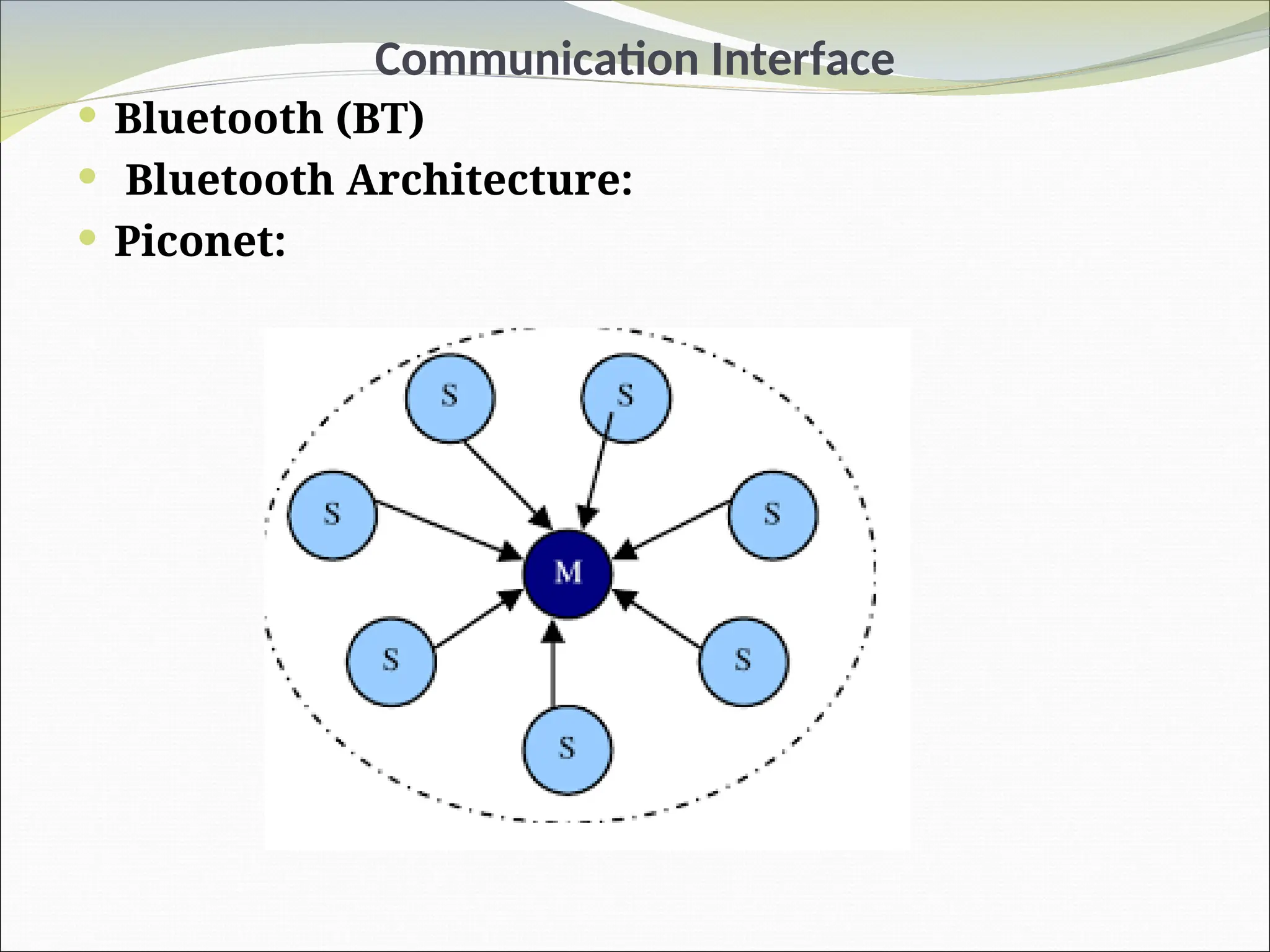
1.Piconet:
Piconet is a type of Bluetooth network that contains one
primary node called the master node and seven active
secondary nodes called slave nodes.
Thus, we can say that there is a total of 8 active nodes
which are present at a distance of 10 meters.
The communication between the primary and secondary
nodes can be one-to-one or one-to-many
Communication Interface
Bluetooth(BT)
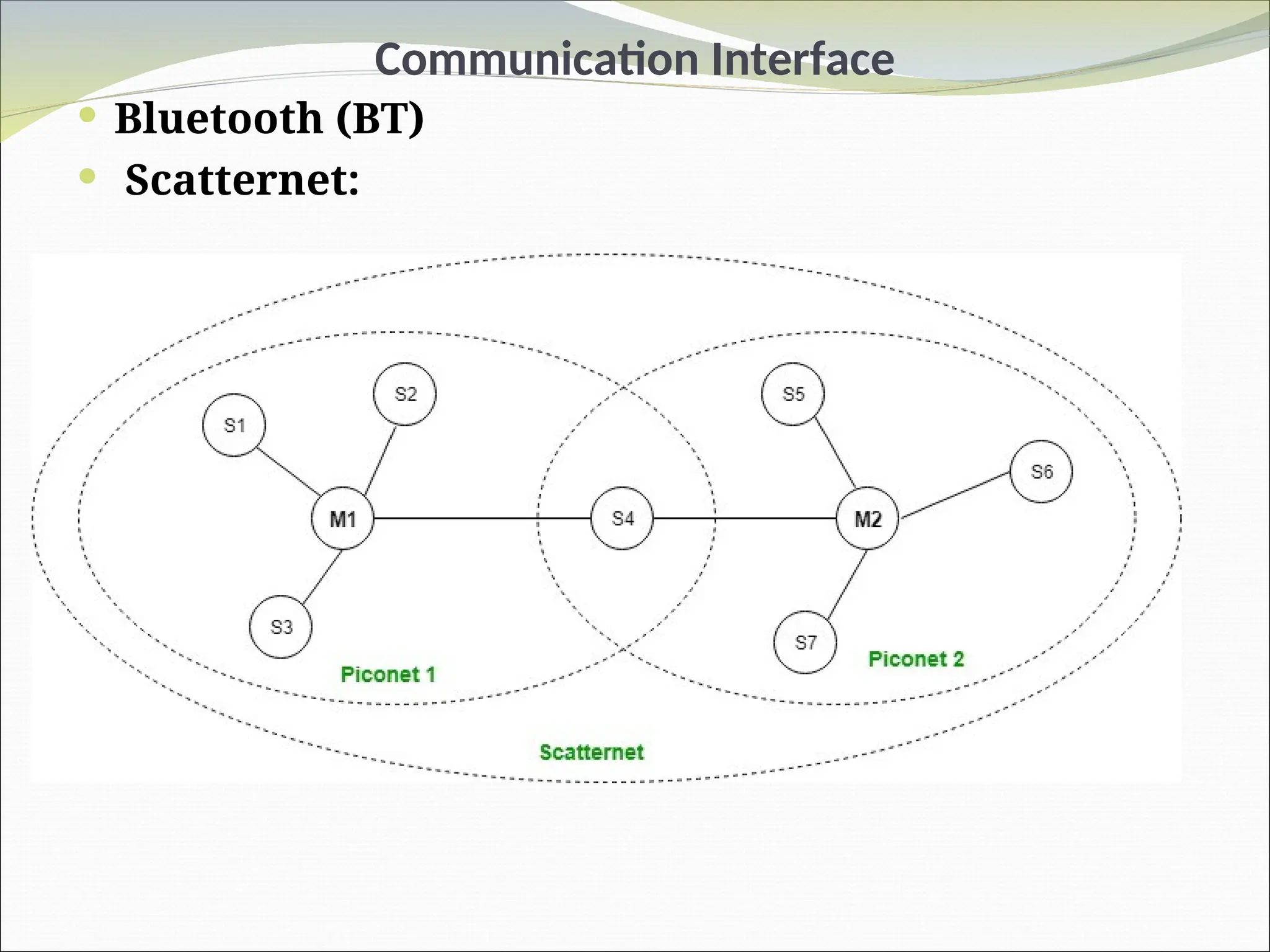
2.Scatternet:
It is formed by using various piconets.
A slave that is present in one piconet can act as
master or we can say primary in another piconet.
This kind of slave (or node )can receive a message
from a master in one piconet and deliver the message
to its slave in the other piconet where it is acting as a
master
Communication Interface
Wi-Fi
Wi-Fi or Wireless Fidelity is the popular wireless
communication technique for networked
communication of devices.
Wi-Fi follows the IEEE 802.11 standard.
IEEE - Institute of Electrical and Electronics Engineers
professional association for electronics
engineering, electrical engineering
journals and conference proceedings, the IEEE also
publishes tutorials and standards t
160.
Communication Interface
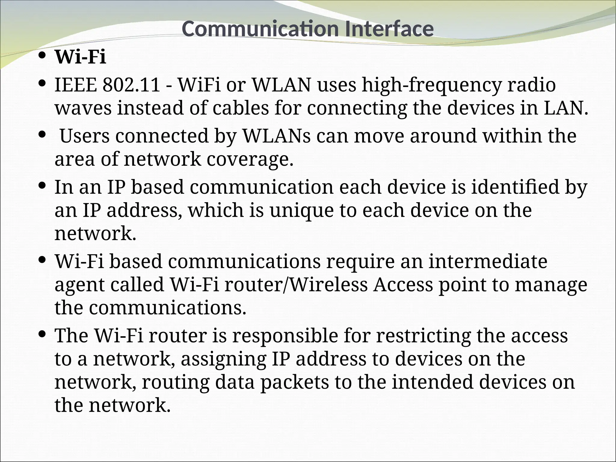
Wi-Fi
IEEE 802.11 - WiFi or WLAN uses high-frequency radio
waves instead of cables for connecting the devices in LAN.
Users connected by WLANs can move around within the
area of network coverage.
In an IP based communication each device is identified by
an IP address, which is unique to each device on the
network.
Wi-Fi based communications require an intermediate
agent called Wi-Fi router/Wireless Access point to manage
the communications.
The Wi-Fi router is responsible for restricting the access
to a network, assigning IP address to devices on the
network, routing data packets to the intended devices on
the network.
161.
Communication Interface
Featuresof Wi-Fi
Wireless Connectivity: Wi-Fi allows devices to connect
to a network without the use of physical cables,
Mobility
High Speed - high-speed internet access, allowing
users to download and upload data quickly.
Easy Setup: Wi-Fi networks are easy to set up and
configure, requiring minimal technical knowledge
162.
Communication Interface
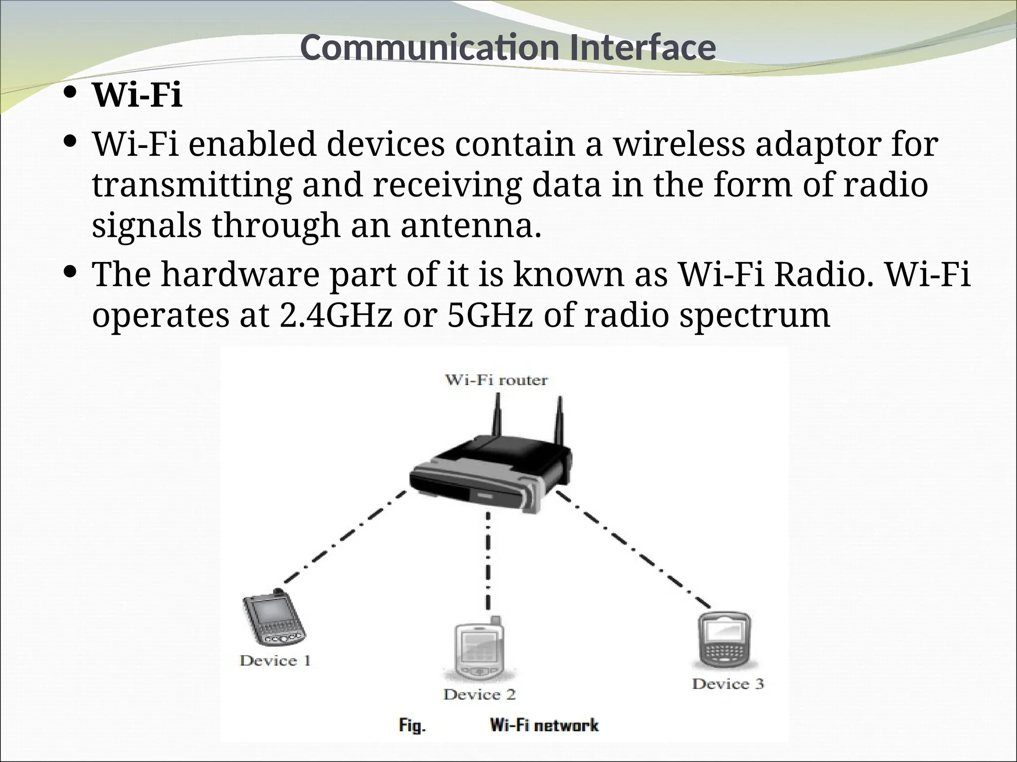
Wi-Fi
Wi-Fi enabled devices contain a wireless adaptor for
transmitting and receiving data in the form of radio
signals through an antenna.
The hardware part of it is known as Wi-Fi Radio. Wi-Fi
operates at 2.4GHz or 5GHz of radio spectrum
163.
Communication Interface
Wi-Fi
Wi-Fi supports data rates ranging from 1 Mbps to 1300
Mbps depending on the standards (802.11a/b/g/n/ac)
and access/ modulation method
Depending on the type of antenna and usage location
(indoor/outdoor), Wi-Fi offers a range of 100 to 1000
feet.
164.
Communication Interface
Wi-Fi
For communicating with devices over a Wi-Fi
network, the device when its Wi-Fi radio is turned ON,
searches the available WiFi network in its vicinity
Lists out the Service Set Identifier (SSID) of the
available networks
If the network is security enabled, a password may be
required to connect to a particular SSID
Wi-Fi supports data rates ranging from 1 Mbps to 1300
Mbps depending on the standards (802.11a/b/g/n/ac)
and access/ modulation method
Depending on the type of antenna and usage location
(indoor/outdoor), Wi-Fi offers a range of 100 to 1000
feet.
165.
Communication Interface
ZigBee
ZigBeeis a low power, low cost, wireless network
communication protocol
Based on the IEEE 802.15.4-2006 standard.
ZigBee is targeted for low power, low data rate and
secure applications for Wireless Personal Area
Networking (WPAN).
WPAN - Connection between the devices happens
within the building or in a room (short range)
The interconnected devices are centered around a
person’s workspace and connected through wireless
medium.
166.
Communication Interface
ZigBee
TheZigBee specifi cations support a robust mesh
network containing multiple nodes.
This networking strategy makes the network reliable
by permitting messages to travel through a number of
different paths to get from one node to another
ZigBee operates worldwide at 2.400 to 2.484 GHz, 902
to 928 MHz and 868.0 to 868.6 MHz.
ZigBee Supports an operating distance of up to 100
metres
Data rate of 20 to 250Kbps
Communication Interface
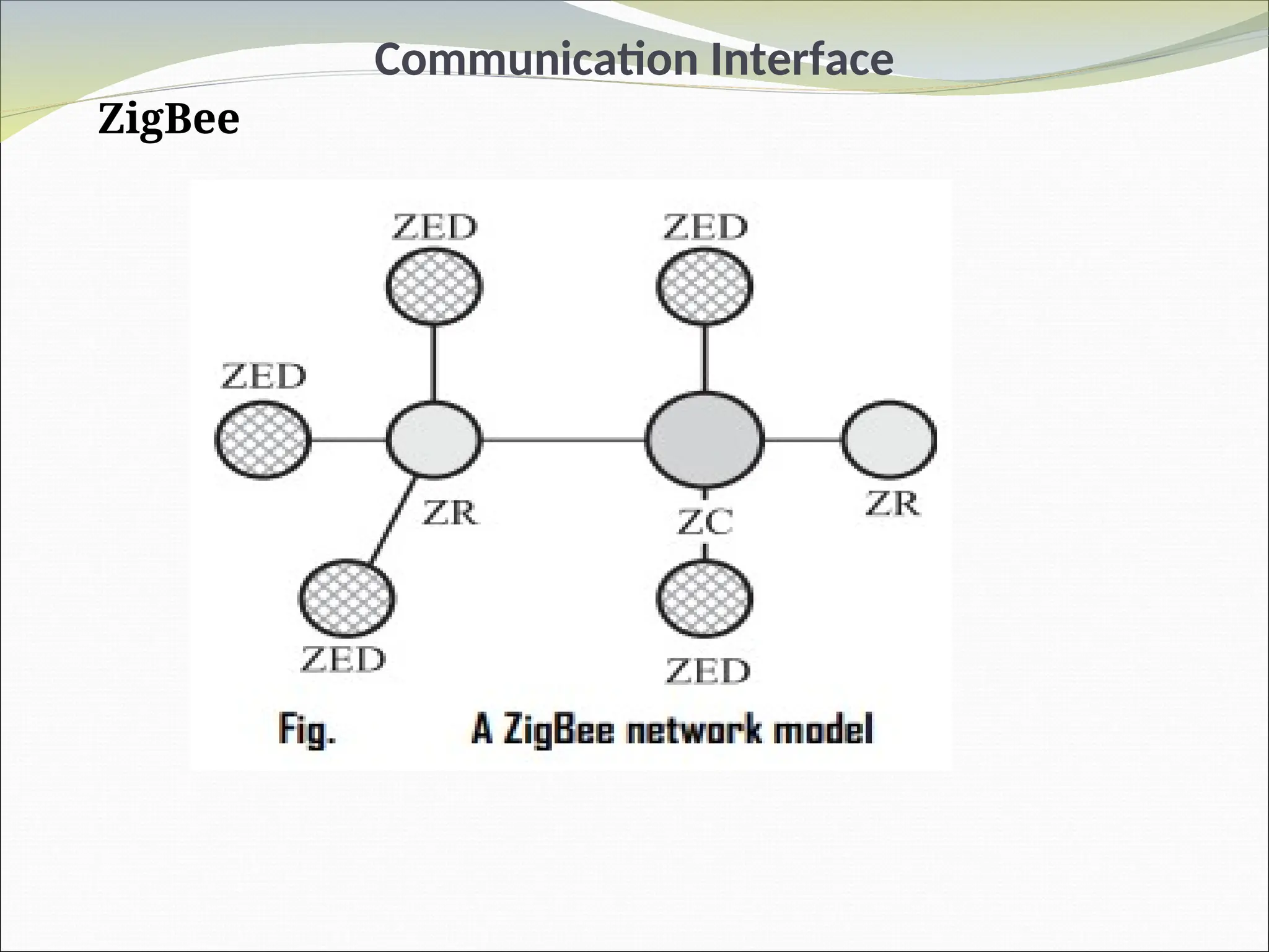
ZigBee
ZigBeeCoordinator (ZC)/Network Coordinator
The ZigBee coordinator acts as the root of the ZigBee
network.
The ZC is responsible for initiating the ZigBee network and
it has the capability to store information about the
network.
ZigBee Router (ZR)/Full func on Device (FFD)
Responsible for passing information from device to
another device or to another ZR.
ZigBee End Device (ZED)/Reduced Func on Device (RFD)
End device containing ZigBee functionality for data
communication. It can talk only with a ZR or ZC and
doesn’t have the capability to act as a mediator for
transferring data from one device to another.
169.
Communication Interface
ZigBee
ZigBeeis primarily targeting application areas like
home & industrial automation, energy management,
home control/security, medical/patient tracking,
logistics & asset tracking and sensor networks & active
RFID
170.
Communication Interface
General PacketRadio Service (GPRS), 3G, 4G, LTE
General Packet Radio Service (GPRS), 3G, 4G and LTE
are cellular communication technique for transferring
data over a mobile communication network like GSM
and CDMA.
Data is sent as packets in GPRS communication.
The transmitting device splits the data into several
related packets.
At the receiving end the data is re-constructed by
combining the received data packets.
GPRS supports a theoretical maximum transfer rate of
171.2kbps
171.
Communication Interface
General PacketRadio Service (GPRS), 3G, 4G, LTE
The radio channel is concurrently shared between
several users instead of dedicating a radio channel to
a cell phone user.
The GPRS communication divides the channel into 8
timeslots and transmits data over the available
channel
GPRS is an old technology and it is being replaced by
new generation cellular data communication
techniques like 3G (3rd Generation), 4G (4th
Generation), LTE (Long Term Evolution) etc. which
offers higher bandwidths for communication.
172.
Communication Interface
General PacketRadio Service (GPRS), 3G, 4G, LTE
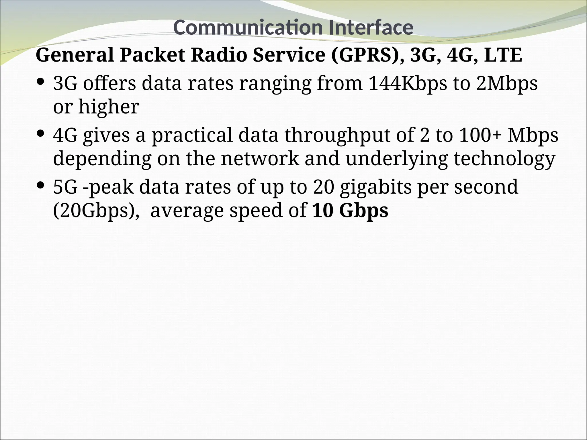
3G offers data rates ranging from 144Kbps to 2Mbps
or higher
4G gives a practical data throughput of 2 to 100+ Mbps
depending on the network and underlying technology
5G -peak data rates of up to 20 gigabits per second
(20Gbps), average speed of 10 Gbps
173.
OTHER SYSTEM COMPONENTS
OTHERSYSTEM COMPONENTS
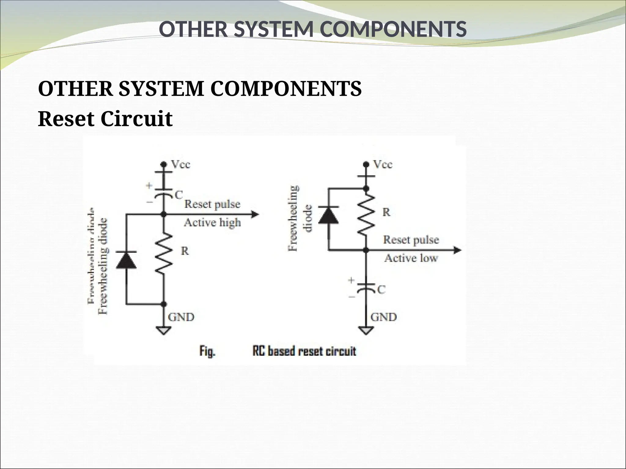
Reset Circuit
It is a circuit that provides a predictable, regulated
voltage to a microprocessor or microcontroller with
the initial application of power
The reset signal can be either active high (The
processor undergoes reset when the reset pin of the
processor is at logic high) or active low (The processor
undergoes reset when the reset pin of the processor is
at logic low)
OTHER SYSTEM COMPONENTS
OTHERSYSTEM COMPONENTS
Reset Circuit
The reset signal can be either active high (The
processor undergoes reset when the reset pin of the
processor is at logic high) or active low (The processor
undergoes reset when the reset pin of the processor is
at logic low)
The reset signal to the processor can be applied at
power ON through an external passive reset circuit
comprising a Capacitor and Resistor or through a
standard Reset IC like MAX810 from Maxim Dallas
(www.maxim-ic.com)
176.
OTHER SYSTEM COMPONENTS
Brown-outProtection Circuit
Brown-out protection circuit prevents the
processor/controller from unexpected program
execution behaviour when the supply voltage to the
processor/controller falls below a specifi ed voltage
Many microcontrollers have a protection circuit
which detects when the supply voltage goes below this
level and puts the device into a reset state to ensure
proper startup when power returns.
This action is called a “Brown Out Reset” or BOR.
177.
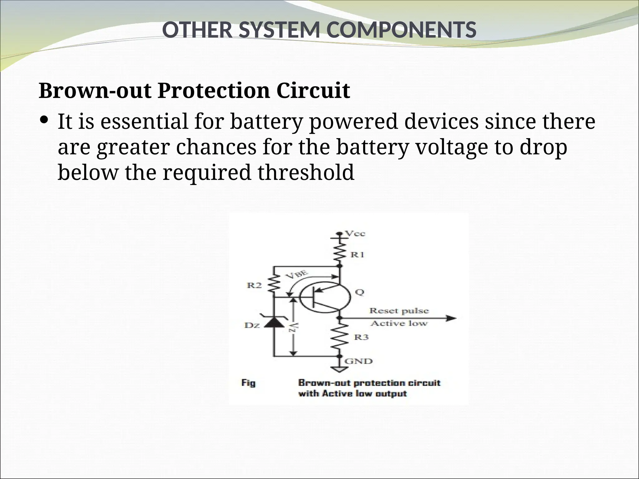
OTHER SYSTEM COMPONENTS
Brown-outProtection Circuit
It is essential for battery powered devices since there
are greater chances for the battery voltage to drop
below the required threshold
178.
OTHER SYSTEM COMPONENTS
Brown-outProtection Circuit
It may lead to situations like data corruption.
A brown-out protection circuit holds the
processor/controller in reset state, when the operating
voltage falls below the threshold, until it rises above
the threshold voltage.
The Zener diode Dz and transistor Q forms the heart
of this circuit.
The transistor conducts always when the supply
voltage Vcc is greater than that of the sum of VBE and
Vz (Zener voltage).
179.
OTHER SYSTEM COMPONENTS
Brown-outProtection Circuit
The transistor stops conducting when the supply
voltage falls below the sum of VBE and Vz.
Select the Zener diode with required voltage for
setting the low threshold value for Vcc.
The values of R1, R2, and R3 can be selected based on
the electrical characteristic
180.
OTHER SYSTEM COMPONENTS
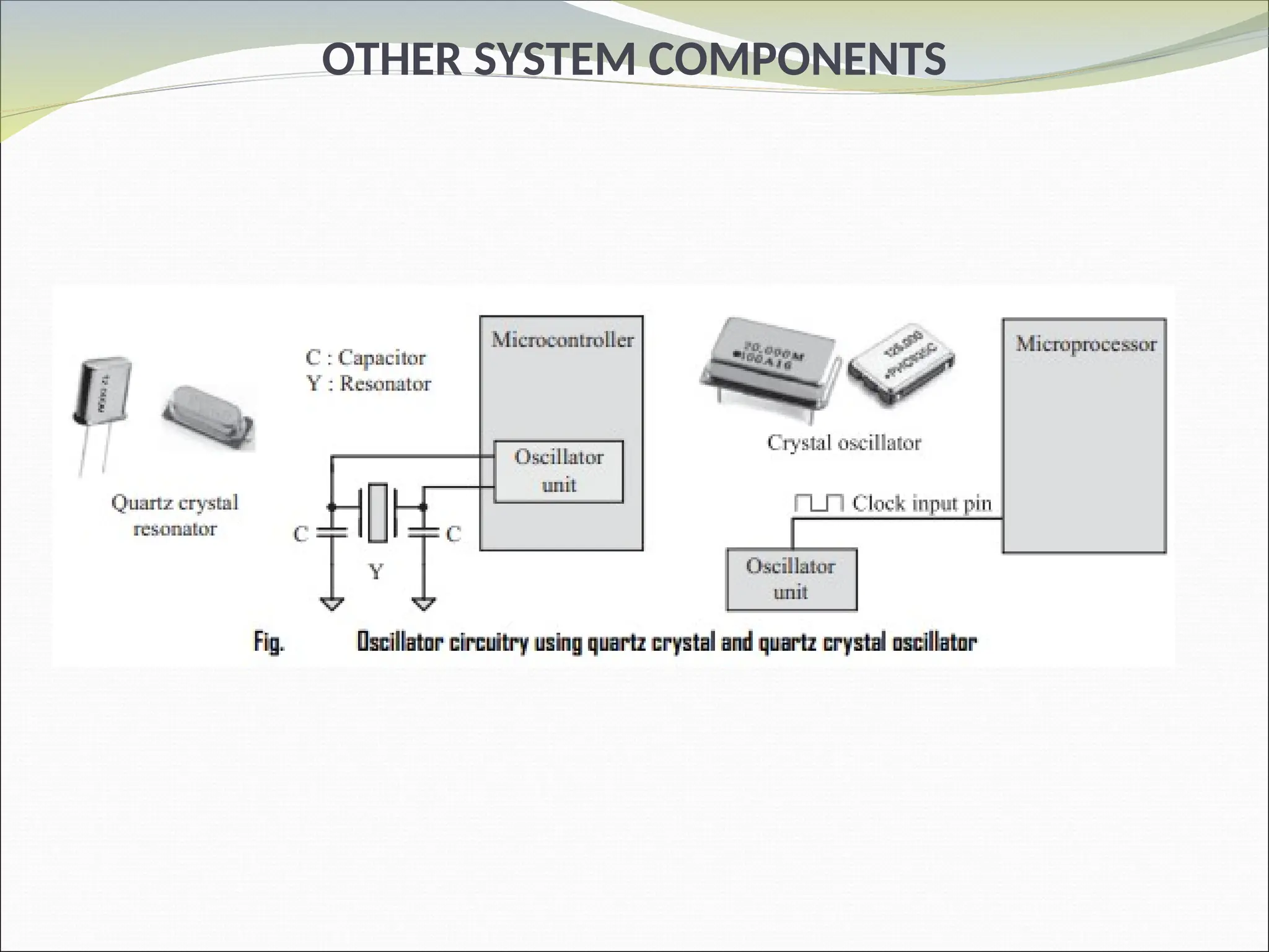
OscillatorUnit
A microprocessor/microcontroller is a digital device
made up of digital combinational and sequential
circuits.
The instruction execution of a
microprocessor/controller occurs in sync with a clock
signal.
It is analogous to the heartbeat of a living being which
synchronises the execution of life.
For a living being, the heart is responsible for the
generation of the beat whereas the oscillator unit of
the embedded system is responsible for generating
the precise clock for the processor.
181.
OTHER SYSTEM COMPONENTS
OscillatorUnit
Certain processors/controllers integrate a built-in
oscillator unit and simply require an external ceramic
resonator/quartz crystal for producing the necessary
clock signals.
The speed of operation of a processor is primarily
dependent on the clock frequency.
However we cannot increase the clock frequency
blindly for increasing the speed of execution.
OTHER SYSTEM COMPONENTS
OscillatorUnit
The logical circuits lying inside the processor always
have an upper threshold value for the maximum clock
at which the system can run, beyond which the
system becomes unstable and non functional.
The total system power consumption is directly
proportional to the clock frequency.
The power consumption increases with increase in
clock frequency
184.
OTHER SYSTEM COMPONENTS
Real-TimeClock (RTC)
Real-Time Clock ( RTC) is a system component
responsible for keeping track of time.
RTC holds information like current time (In hours,
minutes and seconds) in 12 hour/24 hour format, date,
month, year, day of the week, etc. and supplies timing
reference to the system.
RTC is intended to function even in the absence of
power
The RTC chip contains a microchip for holding the
time and date related information and backup battery
cell for functioning in the absence of power, in a
single IC package
185.
OTHER SYSTEM COMPONENTS
Real-TimeClock (RTC)
It is powered by an internal lithium battery.
As a result of which even if the power of the system is
turned off, the RTC clock keeps running.
RTC maintains its clock by counting the cycles of an
oscillator — usually an external 32.768kHz crystal
oscillator circuit, an internal capacitor-based
oscillator, or even an embedded quartz crystal
186.
OTHER SYSTEM COMPONENTS
WatchdogTimer
A watchdog timer (WDT) is a timer that monitors
microcontroller (MCU) programs to see if they are out
of control or have stopped operating.
It acts as a “watchdog” watching over MCU operation.
Watchdog timer is used to generates system reset
if system gets stuck somewhere i.e. if system goes
into endless loop of execution watchdog timer will
reset the system to come out of endless loop.
187.
OTHER SYSTEM COMPONENTS
WatchdogTimer
Watchdog is basically a counter, which starts from
counting zero and reaches to a certain value.
If counter reaches to certain value then watchdog
hardware will generates a watchdog reset.
To avoid system reset, software needs to kick the
watchdog i.e. need to reset the counter to zero
A watchdog timer, or simply a watchdog, is a
hardware timer for monitoring the firmware
execution
188.
OTHER SYSTEM COMPONENTS
WatchdogTimer
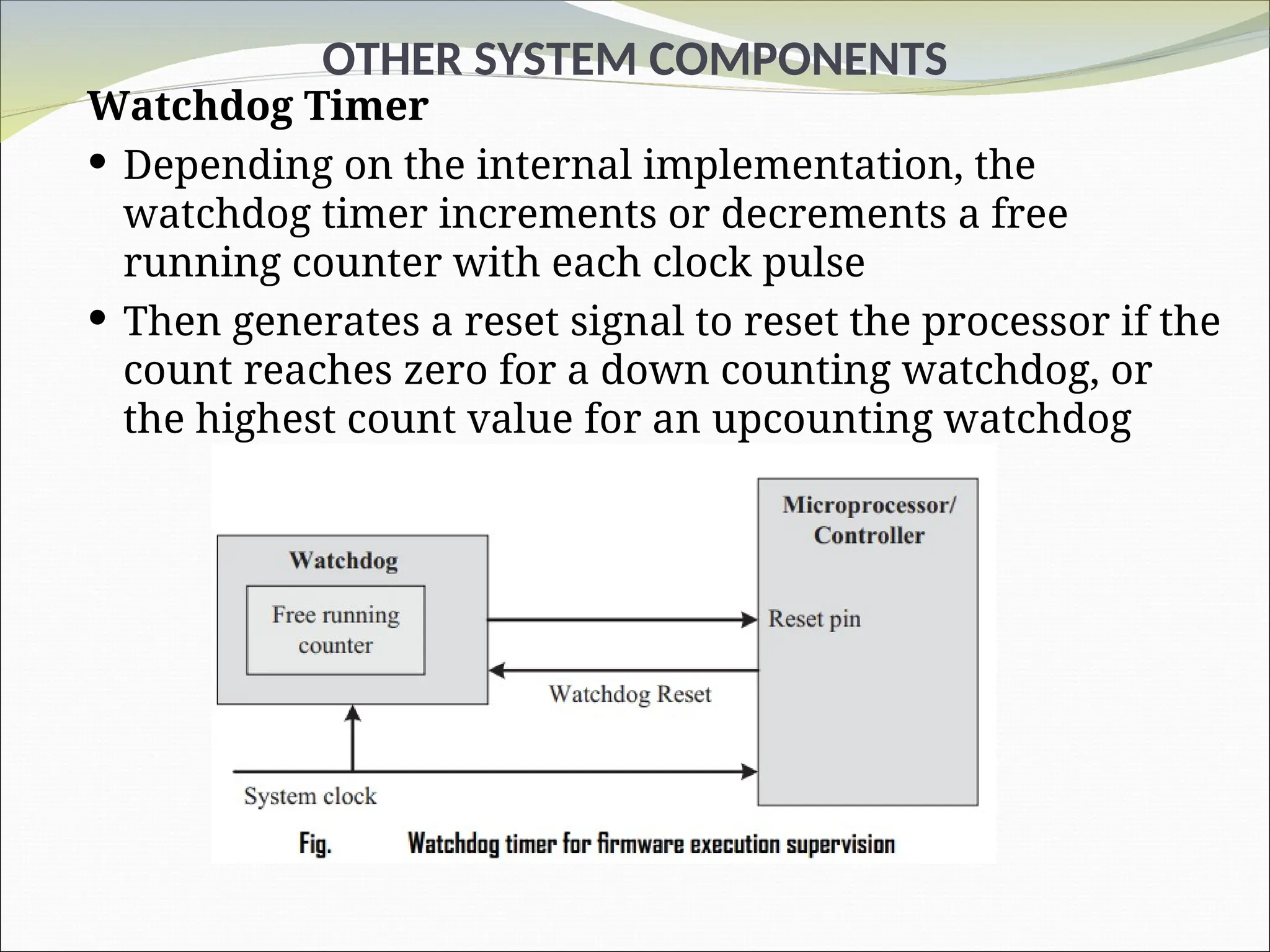
Depending on the internal implementation, the
watchdog timer increments or decrements a free
running counter with each clock pulse
Then generates a reset signal to reset the processor if the
count reaches zero for a down counting watchdog, or
the highest count value for an upcounting watchdog
189.
OTHER SYSTEM COMPONENTS
WatchdogTimer
If the watchdog counter is in the enabled state,
the firmware can write a zero (for upcounting
watchdog implementation) to it before starting the
execution of a piece of code (subroutine or portion of
code which is susceptible to execution hang up) and
the watchdog will start counting.
If the firmware execution doesn’t complete due to
malfunctioning, within the time required by the
watchdog to reach the maximum count, the counter
will generate a reset pulse and this will reset the
processor


![ANPARA THERMAL POWER STATION[1] sangam.pdf](https://cdn.slidesharecdn.com/ss_thumbnails/anparathermalpowerstation1sangam-251121115219-9261cde4-thumbnail.jpg?width=640&height=640&fit=bounds)


